ADC/DAC
מוצרים (2,700+)
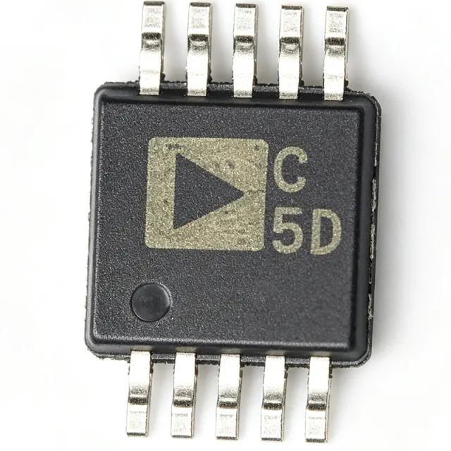
AD7980BRMZ - 16-Bit 1 MSPS PulSAR ADC | Analog Devices
The Analog Devices AD7980BRMZ is a 16-bit, 1 MSPS successive approximation register (SAR) analog-to-digital converter housed in a compact 10-lead MSOP package. It operates from a single VDD supply and contains a low-power, high-speed 16-bit sampling ADC with a versatile SPI-compatible serial interface. The pseudo-differential analog input range extends from 0 V to VREF, where VREF is applied externally and can be set independent of VDD. According to the AD7980 datasheet (Rev. G), the part is pin-for-pin compatible with the 18-bit AD7982. A SAR ADC is an analog-to-digital converter that determines the output code using a binary-search algorithm, comparing the held input against a DAC output one bit at a time. SAR ADCs balance resolution, speed, power, and small size, making them a common choice in precision data acquisition systems. Within the converter hierarchy, the AD7980 is a PulSAR ADC, a proprietary Analog Devices architecture optimized for low power and high accuracy. It sits in the broader signal-chain hierarchy of sensor → signal conditioning → ADC → digital host. Key features include 16-bit resolution with no missing codes, maximum INL of ±1.25 LSB, and a throughput of 1 MSPS. The device supports a pseudo-differential input for common-mode noise rejection, an external reference for flexible full-scale range selection, and a 3-wire SPI interface with daisy-chain capability and an optional BUSY indicator. The digital interface is compatible with 1.8 V to 5 V logic families, easing connection to a wide range of microcontrollers and FPGAs. Architecturally, the AD7980 uses an internal capacitor DAC and low-power comparator to achieve fast conversion while maintaining excellent linearity. Power dissipation scales linearly with throughput, which is advantageous in battery-powered and duty-cycled systems. The small 10-MSOP package and exposed pad provide space savings and flexible layout options for dense printed-circuit boards. Typical applications include industrial control, medical instrumentation, automated test equipment, precision sensor signal chains, and PLC analog input modules. The combination of 16-bit resolution, 1 MSPS speed, low power, and an SPI interface makes it suitable for multichannel systems where small board area is required. Designers should provide a low-impedance reference source, a driver amplifier with adequate settling time, and careful decoupling on VDD and VIO for best performance.
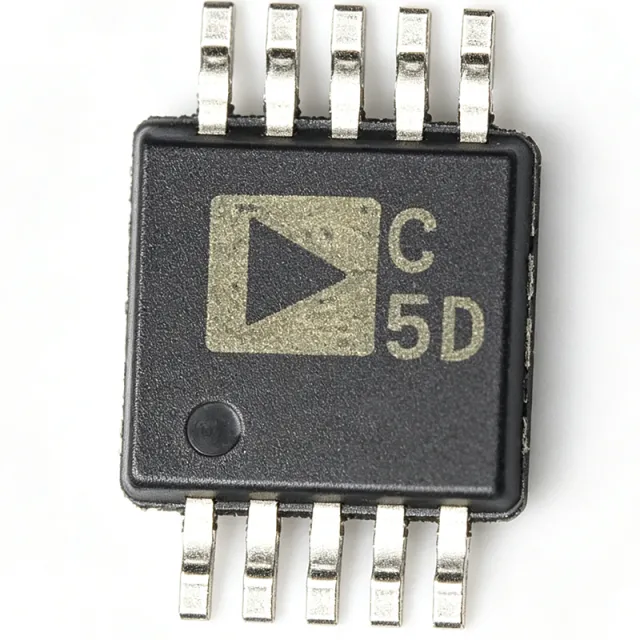
AD7980BRMZRL7 - 16-Bit 1 MSPS PulSAR ADC | Analog Devices
The Analog Devices AD7980BRMZRL7 is a 16-bit, 1 MSPS successive approximation register (SAR) analog-to-digital converter in a 10-lead MSOP package with a -7-inch reel option for high-volume assembly. It operates from a single 2.5 V to 5.5 V supply (VDD), supports a pseudo-differential analog input range of 0 V to VREF where VREF can be set independently between 2.5 V and 5 V, and delivers zero-latency 16-bit conversion with no missing codes at full throughput. What is a SAR ADC? A Successive Approximation Register ADC is a class of analog-to-digital converter that uses a binary search algorithm together with a charge-redistribution DAC to step toward the digital representation of the input voltage one bit per clock cycle. SAR ADCs are valued for their deterministic behavior, zero pipeline latency, low power consumption, and excellent DC linearity, and they occupy the role of mid-speed precision converter within the broader hierarchy: SAR ADC -> ADC -> data converter -> mixed-signal IC -> semiconductor. Key features of the AD7980BRMZRL7 include ±0.6 LSB typical INL (1.25 LSB max), 91.5 dB SNR and 92 dB dynamic range at VREF = 5 V, an SPI-compatible serial port that supports daisy-chaining multiple ADCs on a 3-wire bus via the SDI input, and an optional BUSY indicator. The digital I/O is compatible with 1.8 V to 5 V logic families, allowing direct connection to modern MCUs and FPGAs without level shifters. The AD7980 uses a low-noise, fully differential charge-redistribution DAC core combined with a precision comparator and SAR logic, achieving 16-bit resolution while consuming only a few milliwatts at full 1 MSPS throughput. Power consumption scales linearly with sample rate, enabling sub-mW operation when the part is clocked down for battery-powered or thermal-sensitive designs. The 10-lead MSOP footprint measures approximately 3 mm x 3 mm, making the part suitable for dense, multi-channel data-acquisition boards. Typical applications include precision industrial process control loops, portable medical instrumentation, multi-channel data-acquisition modules, optical networking feedback loops, and battery-powered measurement front ends. The combination of 1 MSPS throughput, low power, and small footprint makes it ideal for distributed sensing nodes and high-density plug-in cards. When designing with the AD7980, drive the analog input with a low-impedance buffer to minimize kickback and aperture uncertainty, decouple VREF with high-quality ceramic capacitance, and route the serial lines with short, impedance-controlled traces to preserve acquisition timing margins. This page synthesizes distributor pricing as of 2026-10-06, drop-in same-package alternatives sourced from Analog Devices' own PulSAR family, and practical design notes not aggregated on any single distributor page.

AD7982BCPZ - 18-Bit 1 MSPS PulSAR ADC | Analog Devices
The AD7982BCPZ is an 18-bit, successive approximation register (SAR) analog-to-digital converter (ADC) from Analog Devices, offering a maximum throughput of 1 MSPS. It operates from a single 2.5 V supply (VDD) and features a separate VIO supply for digital interface compatibility with 1.8 V, 2.5 V, 3 V, or 5 V logic. The device is available in a 10-lead LFCSP-WD (3x3 mm) package, specified for operation from -40°C to +85°C. A SAR ADC is a type of analog-to-digital converter that uses a binary search algorithm to convert an analog input into a digital output. It typically offers high resolution, low power consumption, and fast conversion times, making it suitable for applications requiring precise measurements with moderate sampling rates. SAR ADCs are widely used in data acquisition systems, industrial process control, medical instrumentation, and portable devices. Key features of the AD7982 include 18-bit resolution with no missing codes, a throughput of 1 MSPS, and low power dissipation. At 1 MSPS, the power consumption is typically 7.5 mW, while at 10 kSPS it drops to 75 µW, making it ideal for battery-powered applications. The device achieves an integral nonlinearity (INL) of ±1 LSB typical and ±2 LSB maximum, and a dynamic range of 99 dB. It also features a versatile serial interface port that is compatible with SPI, QSPI, MICROWIRE, and DSP interfaces. The AD7982 uses a low-power, high-speed 18-bit sampling ADC architecture with a capacitive DAC and a precision comparator. The device includes an internal reference buffer and supports both external and internal reference options. The serial interface provides a daisy-chain mode for multiple ADC configurations, simplifying system design. The LFCSP package offers excellent thermal performance and a compact footprint for space-constrained designs. Typical applications include high-speed data acquisition, industrial process control, medical imaging, and portable instrumentation. The low power consumption and high resolution make it suitable for battery-powered devices, while the high throughput supports real-time monitoring systems. The device is also used in vibration analysis, motor control, and other precision measurement applications. When designing with the AD7982, ensure proper decoupling of the VDD and VIO supplies with 100 nF and 10 µF capacitors placed close to the pins. The reference input should be bypassed with a 10 µF capacitor to maintain stability. The serial clock (SCK) frequency should not exceed 50 MHz to ensure reliable data transfer. The device supports power-down modes to reduce power consumption further when not converting.
AD7983BCPZ-R2 - 16-Bit 1.33 MSPS PulSAR ADC | Analog Devices
The Analog Devices AD7983BCPZ-R2 is a 16-bit, 1.33 MSPS successive-approximation register (SAR) analog-to-digital converter in a 10-lead LFCSP-WD (3x3 mm) package with an exposed pad for improved thermal dissipation. It operates from a single 2.5 V to 5.5 V supply (VDD), consumes 10.5 mW typical at full throughput, and provides true 16-bit performance with no missing codes. The integrated PulSAR core delivers ±0.6 LSB typical INL and 91 dB SINAD, while the versatile serial interface is compatible with 1.8 V to 5 V digital logic. A successive-approximation register ADC is a precision data-conversion architecture that uses a binary-search algorithm against an internal DAC to resolve each analog sample into a digital value, achieving an excellent balance of speed, accuracy, and power for medium-bandwidth measurement channels. In the broader taxonomy, the AD7983 belongs to the SAR ADC family within precision data converters, which sits alongside delta-sigma and pipeline converters; delta-sigma favors highest resolution at low bandwidth, while SAR excels at sub-MHz to multi-MHz signals with low latency, making SAR the standard choice for instrumentation, motor control, and multi-channel multiplexed data-acquisition front ends. Key features include a 0 V to REF pseudo-differential input range with ground sense (IN-), an external reference voltage (REF), a hardware CNV (convert) input that initiates acquisition on the rising edge, and an SCK-driven serial data output. The LFCSP-WD (3x3) footprint with a wettable flank enables optical inspection on the PCB. The AD7983 is pin-for-pin compatible with the 18-bit AD7982 and the 16-bit AD7689/AD7699 family, giving designers an upgrade/downgrade path on a single PCB layout. Typical applications include industrial process control loop measurement, battery monitoring and management systems (BMS), precision instrumentation and data acquisition modules, motor control feedback via shunt current sensing, and portable medical devices. The 1.33 MSPS throughput and low power make it particularly attractive for battery-powered multi-channel scanning systems where acquisition speed and accuracy must coexist with strict thermal and energy budgets. When designing with the AD7983BCPZ-R2, place the REF decoupling capacitor (typically 10 uF ceramic in parallel with a 0.1 uF) directly at the REF pin, and use a low-impedance ground pour tied to the exposed pad to minimize reference noise coupling. The serial interface timing budget should be respected per the datasheet timing diagram; SCK frequencies up to 50 MHz are supported, allowing easy FPGA and modern MCU host interfacing.

AD7983BCPZ-RL - 16-Bit 1.33 MSPS SAR ADC LFCSP-10 | ADI
The Analog Devices AD7983BCPZ-RL is a 16-bit, 1.33 MSPS successive-approximation analog-to-digital converter (ADC) in a 10-lead LFCSP-WD (3x3 mm) package with exposed die pad. It operates from a single 2.5 V supply, draws 10.5 mW typical at 1.33 MSPS, and is pin-for-pin compatible with the 18-bit AD7982. An SAR ADC is a precision data converter that uses an iterative binary-search algorithm with an internal capacitive DAC to digitize an analog input one bit per clock cycle. SAR ADCs deliver deterministic latency, no pipeline delay, and excellent DC accuracy, making them the preferred topology for multiplexed data-acquisition systems, precision instrumentation, and industrial control loops where deterministic per-sample timing and low noise are mandatory. Key specifications include 16-bit resolution with no missing codes, ±0.6 LSB typical ( ±1.0 LSB maximum ) INL, throughput of 1.33 MSPS, and a versatile serial interface that can be wired to 1.8 V to 5 V digital logic. The analog input is sampled differentially between IN+ and IN-, with the full-scale range set by an external REF voltage from 2.375 V to 2.625 V. CNV rising-edge triggering initiates conversion, and the on-chip oscillator eliminates the need for an external clock source. The architecture pairs a low-power, high-speed sampling front end with an internal precision reference buffer and a compact serial output that minimizes GPIO usage on the host MCU or DSP. Power-down between conversions reduces average dissipation in low-duty-cycle applications, and the -40 °C to +85 °C industrial operating range supports factory-floor deployment. Typical applications include portable and battery-powered instrumentation, process-control analog front ends, data-acquisition modules, and precision sensor signal chains. The wide logic compatibility and small footprint also suit medical monitoring and industrial IoT edge nodes. When designing with the AD7983BCPZ-RL, bypass VDD and REF with 10 µF and 100 nF ceramic capacitors placed within 5 mm of the package, and keep the analog input traces short and guarded. The exposed pad must be soldered to the ground plane for thermal dissipation and low-impedance return. This page synthesizes distributor pricing, drop-in alternatives in the same LFCSP-10 footprint, and design notes that complement the Analog Devices datasheet.
AD7984BCPZ - 18-Bit 1.33 MSPS SAR ADC | Analog Devices
The AD7984BCPZ is an 18-bit, 1.33 MSPS successive approximation register (SAR) analog-to-digital converter (ADC) from Analog Devices, part of the PulSAR family. It operates from a single 2.5 V supply and dissipates only 10.5 mW at full throughput, making it ideal for power-sensitive precision data acquisition systems. The device is available in a 10-lead LFCSP-WD (3x3 mm) package, offering a compact footprint for space-constrained designs. A SAR ADC is a type of analog-to-digital converter that uses a binary search algorithm to convert an analog input into a digital code. It employs a comparator and a digital-to-analog converter (DAC) to successively approximate the input voltage, achieving high resolution and speed with low power consumption. SAR ADCs are widely used in applications requiring high precision and moderate sampling rates, such as industrial process control, medical instrumentation, and scientific analysis. Key features of the AD7984BCPZ include 18-bit resolution with no missing codes, a true differential analog input range of ±VREF with VREF between 5.0 V, and an INL of ±2.25 LSB maximum. It offers a dynamic range of 99.7 dB typical and a signal-to-noise ratio (SNR) of 99 dB typical. The device features an SPI-compatible serial interface that supports daisy-chaining multiple ADCs on a single 3-wire bus and provides an optional busy indicator. The reference voltage is applied externally and can be set independent of the supply voltage. The AD7984BCPZ is pin-for-pin compatible with the 18-bit AD7982, allowing easy upgrades or substitutions in existing designs. It can interface with any 1.8 V to 5 V digital logic family, providing flexibility in mixed-voltage systems. The device operates over a temperature range of -40°C to +125°C, making it suitable for harsh industrial environments. Typical applications include high-speed data acquisition, medical imaging, spectroscopy, and vibration analysis. Its low power dissipation and high accuracy make it particularly well-suited for battery-powered portable instruments and remote sensing nodes. When designing with the AD7984BCPZ, ensure a clean, low-impedance reference voltage source and adequate decoupling on the VDD and REF pins. The SPI interface should be kept short to minimize noise, and the analog input should be driven by a low-impedance source to maintain accuracy.

AD7986BCPZ - 18-Bit 2 MSPS SAR ADC | Analog Devices
The AD7986BCPZ is an 18-bit, 2 MSPS successive approximation register (SAR) analog-to-digital converter (ADC) from Analog Devices, packaged in a 20-lead LFCSP (4x4 mm). It operates from a single 2.5 V supply and features a separate VIO supply for digital interface compatibility with 1.8 V, 2.5 V, and 2.7 V logic. The device consumes only 15 mW at 2 MSPS, making it ideal for high-speed, low-power data acquisition systems. An ADC (analog-to-digital converter) is an electronic component that converts continuous analog signals into discrete digital numbers, enabling digital processing and storage. SAR ADCs use a binary search algorithm to determine the digital output, offering a good balance of speed, resolution, and power consumption. The AD7986 belongs to the PulSAR family, known for high accuracy and low noise, and is used in applications such as medical imaging, industrial process control, and scientific instrumentation. Key features include a 2 MSPS throughput, 18-bit resolution, and a typical signal-to-noise ratio (SNR) of 98 dB. The device supports both SPI and daisy-chain serial interfaces, allowing multiple ADCs to be connected to a single bus. It also includes a busy indicator and a conversion result readback feature. The LFCSP package provides excellent thermal performance and a small footprint for space-constrained designs. The AD7986 uses a charge redistribution architecture with an internal reference buffer, achieving high linearity and low drift. The device operates over the industrial temperature range of -40°C to +85°C. Its low power dissipation and high speed make it suitable for portable and battery-powered instruments where power efficiency is critical. Typical applications include high-speed data acquisition, medical imaging (e.g., ultrasound), industrial automation, and test and measurement equipment. The device's high SNR and low distortion ensure accurate signal reproduction in demanding environments. When designing with the AD7986, ensure proper decoupling of the AVDD and DVDD supplies, and use a low-noise reference voltage source. The VIO pin must be connected to the appropriate logic level to match the host interface. Careful PCB layout, including a solid ground plane and short trace lengths, is essential to achieve the specified performance.
AD7988-1BCPZ - 16-Bit 100kSPS SAR ADC | Analog Devices
The AD7988-1BCPZ is a 16-bit, successive approximation register (SAR) analog-to-digital converter (ADC) from Analog Devices, offering a 100 kSPS throughput. It operates from a single power supply, VDD, and features a versatile serial interface port that is SPI-compatible. The device is housed in a compact 10-lead LFCSP-WD (3x3 mm) package, making it suitable for space-constrained applications. An ADC (analog-to-digital converter) is a device that converts continuous analog signals into discrete digital numbers. The AD7988-1 is a SAR ADC, which uses a binary search algorithm to determine the digital output. SAR ADCs are known for their high speed, low power consumption, and ease of use. They are widely used in data acquisition systems, industrial process control, and medical instrumentation. The AD7988-1 is part of the PulSAR family of ADCs from Analog Devices, which are recognized for their high performance and low power. Key features of the AD7988-1BCPZ include 16-bit resolution, 100 kSPS sampling rate, and low power consumption. It operates from a single 2.375V to 5.5V supply, and the separate VIO supply allows interface with 1.8V, 2.5V, 3V, or 5V logic. The device also features a daisy-chain capability using the SDI input, enabling multiple ADCs to be connected on a single 3-wire bus. The LFCSP package provides excellent thermal performance and a small footprint. The AD7988-1 uses a capacitive DAC architecture with a precision comparator, achieving high accuracy and low noise. The device includes an internal reference buffer and supports both external and internal reference options. The SPI-compatible serial interface simplifies connection to microcontrollers and DSPs. The device is specified for operation from -40°C to +125°C, making it suitable for industrial and automotive environments. Typical applications include battery-powered instruments, portable medical devices, data acquisition systems, and industrial process control. The low power consumption and small package make it ideal for portable and space-constrained designs. The high resolution and accuracy ensure reliable performance in precision measurement applications. When designing with the AD7988-1, ensure proper decoupling of the VDD and VIO supplies with 0.1uF and 10uF capacitors. The reference input should be bypassed with a 10uF capacitor to maintain stability. The SCLK frequency should be within the specified range to ensure accurate conversion.
AD7988-5BCPZ - 16-Bit 500kSPS SAR ADC | Analog Devices
The AD7988-5BCPZ is a 16-bit, successive approximation register (SAR) analog-to-digital converter (ADC) from Analog Devices, offering a 500 kSPS throughput. It operates from a single power supply, VDD, and features a versatile serial interface port that is SPI-, QSPI-, MICROWIRE-, and DSP-compatible. The device is housed in a 10-lead LFCSP-WD (3x3 mm) package and is specified for operation from -40°C to +125°C. An ADC (analog-to-digital converter) is an electronic component that converts continuous analog signals into discrete digital numbers, enabling digital systems to process real-world signals. SAR ADCs use a binary search algorithm to determine the digital output, offering a good balance of speed, resolution, and power consumption. The AD7988-5 is part of the SAR ADC family, which is widely used in data acquisition systems, industrial process control, and medical instrumentation. Key features of the AD7988-5 include ultra-low power consumption, making it suitable for battery-powered and portable applications. It supports a wide logic interface range from 1.8 V to 5 V via the separate VIO supply, allowing direct connection to various microcontrollers and DSPs. The device also supports daisy-chaining multiple ADCs on a single 3-wire bus using the SDI input, simplifying system design and reducing pin count. The AD7988-5 uses a successive approximation architecture with an internal capacitive DAC, providing high accuracy and low noise. It includes a track-and-hold circuit that captures the input signal, and the conversion result is output serially. The device features a power-down mode to reduce current consumption between conversions, further enhancing its efficiency in duty-cycled applications. Typical applications include battery-powered instrumentation, portable medical devices, data acquisition systems, and industrial process control. Its high throughput and low power make it ideal for applications requiring continuous monitoring of multiple channels, such as multi-channel data loggers and portable analyzers. When designing with the AD7988-5, ensure that the reference voltage is stable and well-decoupled, as it directly affects conversion accuracy. The analog input should be driven by a low-impedance source to avoid sampling errors, and proper PCB layout with separate analog and digital grounds is recommended to minimize noise.

AD7992BRMZ-1-R2 - 12-Bit 2-Ch SAR ADC, I2C, 10-MSOP | Analog Devices
The Analog Devices AD7992BRMZ-1-R2 is a 12-bit, 2-channel successive-approximation analog-to-digital converter (SAR ADC) with an I2C-compatible serial interface, housed in a 10-pin MSOP (RM-10) package. It operates from a single 2.7 V to 5.5 V supply, supports up to 2 I2C addresses, and offers a 2 us conversion time per channel. The -1 variant supports standard, fast, and high-speed I2C modes (up to 3.4 MHz), and ships on a 250-piece reel (suffix -R2). An ADC (analog-to-digital converter) is a data-acquisition IC that samples continuous analog signals and translates them into discrete digital codes for downstream processors, microcontrollers, or FPGAs. SAR ADCs use a successive-approximation register and an internal DAC to perform one bit per clock cycle, achieving deterministic latency that is ideal for multiplexed multi-channel systems. The AD7992 belongs to the broader data-converter hierarchy: ADC -> data converter -> signal chain IC -> mixed-signal semiconductor, sitting between the analog sensor front end and the digital host. Key features include a 2-channel input multiplexer with track-and-hold, an external reference input from 1.2 V to VDD for maximum dynamic range, automatic or command-driven conversion modes controlled via the CONVST pin or the I2C bus, and a wide operating temperature range of -40C to +125C. The device consumes only a few milliwatts in operation and provides excellent DC accuracy for its class. Typical applications include system monitoring and battery-cell monitoring in portable equipment, transducer/sensor signal acquisition, process-control loop read-back, and digital-system analog housekeeping (supply rails, temperature, current). The small 10-MSOP footprint, low power, and I2C connectivity make it a strong fit for space-constrained, multi-rail designs. When designing with the AD7992BRMZ-1-R2, choose the external reference carefully - the input range scales with VREF, so a 5 V reference allows true 0-5 V single-ended or pseudo-differential sensing without external dividers. Decouple VDD with a 0.1 uF ceramic placed within 5 mm of the pin and keep analog/digital grounds joined at a single star point. Pull-up resistors on SDA/SCL must be sized for the chosen I2C speed (4.7 kohm at 400 kHz, 1 kohm at 3.4 MHz). This page consolidates distributor pricing from DigiKey, Mouser, and Octopart, drop-in alternatives that share the 10-MSOP footprint, and practical design notes not included in the manufacturer datasheet.

AD7993BRU-0REEL - 10-Bit 4-CH SAR ADC, I2C, 16-TSSOP
The Analog Devices AD7993BRU-0REEL is a 4-channel, 10-bit, successive-approximation analog-to-digital converter (SAR ADC) that operates from a single 2.7 V to 5.5 V supply and achieves up to 188 kSPS throughput with a typical 2 us conversion time, housed in a 16-lead TSSOP package delivered on tape-and-reel. A SAR ADC is a class of analog-to-digital converter that uses a binary-search successive-approximation register to convert an input sample in N clock cycles for N bits of resolution. SAR ADCs occupy the middle ground between flash ADCs (fast, power-hungry, low resolution) and sigma-delta ADCs (high resolution, slow). They are the workhorse choice for general-purpose data acquisition, sensor readout, and microcontroller/microprocessor monitoring rails where both speed and resolution matter. The AD7993 specifically integrates a four-input multiplexer and track-and-hold amplifier, allowing four analog sources to share one ADC, reducing both BOM cost and PCB area. Key features include four single-ended analog input channels, an I2C-compatible two-wire serial interface (standard, fast, and high-speed modes), 188 kSPS throughput, automatic sequencer operation, a hardware/software shutdown mode, and an automatic cycle interval timer. The wide 2.7 V to 5.5 V supply range permits direct interfacing to both 3.3 V microcontrollers and 5 V legacy systems. Low power consumption makes the part well-suited to battery-aware designs. Architecturally, the AD7993 uses a charge-redistribution DAC core combined with an on-chip input track-and-hold rated for input bandwidths up to 11 MHz. The integrated input multiplexer supports both sequential and per-conversion channel selection. The I2C address is partially hardware-configurable, allowing up to three AD7993s on a single bus. The sequencer can also be set to cycle automatically across all four inputs. Typical applications include system monitoring (board-level voltage, current, and temperature supervision), portable instrumentation, battery-powered sensor readout, multi-cell battery monitoring, and process-control front-ends. The TSSOP-16 footprint drops onto a small footprint that is easy to lay out next to a microcontroller. The wide supply range avoids the need for level shifters on most 5 V analog rails. When designing with this part, ensure that the I2C bus pull-ups match the chosen speed mode (4.7 kohm for standard, lower for fast/high-speed) and that the reference voltage (VDD) is well decoupled with a 10 nF + 1 uF capacitor pair to limit conversion noise. The shutdown current is sub-microamp, so it is safe to leave the ADC off during long idle periods.
AD7994BRU-0REEL - 4-Ch 12-Bit 188kSPS SAR ADC I2C 16-TSSOP
The Analog Devices AD7994BRU-0REEL is a 4-channel, 12-bit successive approximation register (SAR) analog-to-digital converter with an I2C-compatible serial interface, housed in a 16-pin TSSOP package and supplied on a 7-inch reel. A SAR ADC is a type of data converter that performs a binary search through successive approximations against a precision DAC to digitize an analog input, achieving an excellent balance between speed, accuracy, and power consumption for mid-rate applications. Within the broader signal chain hierarchy, the AD7994 sits between the analog front-end (sensors, op-amps, muxes) and the digital controller (microcontroller, FPGA, ASIC), functioning as a power-management-aware mixed-signal IC. ADCs in the 10-12 bit, 100kSPS-1MSPS class are the workhorse of industrial monitoring, portable instrumentation, and embedded sensor readback. Key features of the AD7994BRU-0REEL include a 188 kSPS throughput rate, a 2 microsecond typical conversion time, single 2.7 V to 5.5 V supply operation, and four single-ended analog input channels with a track-and-hold amplifier that supports input bandwidths up to 11 MHz. The device also provides an automatic cycle mode for sequential channel scanning, pin-selectable I2C addressing via the AS pin for bus sharing, and an automatic shutdown mode that reduces supply current to a typical 1 microamp between conversions. Technically, the AD7994 uses a charge-redistribution SAR core with an internal clock derived from the I2C SCL line, eliminating the need for an external crystal or oscillator. The integrated 4-channel analog multiplexer and track-and-hold block allow ratiometric or absolute measurements against VDD, and the wide input bandwidth preserves transient integrity for multiplexed signals. Typical applications include battery monitoring in portable equipment, sensor array reading in industrial control, panel meters and instrumentation, and digital system monitoring of temperature, pressure, or supply rails. Compact 16-lead TSSOP packaging keeps the part footprint compatible with space-constrained designs. When designing with this part, observe the I2C address-scheme strategy (AS pin logic level) to avoid bus conflicts when multiple AD799x devices share the same controller. Decouple VDD with a 0.1 microfarad ceramic capacitor placed as close as possible to the supply pin, and keep analog traces short and guarded by the AGND pin to minimize digital coupling into the conversion result. This page synthesizes distributor pricing, cross-brand drop-in alternatives, and practical design notes that are not collected in the bare manufacturer datasheet.

AD7995YRMZ-0 - 10-Bit SAR ADC, 4-Channel I2C | Analog Devices
The Analog Devices AD7995YRMZ-0 is a 10-bit, low-power, successive approximation (SAR) analog-to-digital converter with an I2C-compatible serial interface, housed in an 8-pin MSOP package. It offers 3 or 4 analog input channels (one input pin doubles as an external reference), 1 µs typical conversion time, and operates from a single 2.7 V to 5.5 V supply. The -0 suffix denotes the specific I2C address variant and the YRMZ industrial/automotive temperature range (-40 °C to +125 °C). A successive approximation ADC (SAR ADC) is a type of analog-to-digital converter that uses a binary search algorithm through an internal DAC to converge on the input voltage in N clock cycles for N-bit resolution. SAR ADCs sit in the data-converter hierarchy under analog-to-digital converters, which themselves belong to the broader mixed-signal / data acquisition IC family. They are favored for their deterministic latency, low power consumption, and ease of use in multiplexed multi-channel applications. The AD7995YRMZ-0 features an integrated track-and-hold amplifier, automatic channel sequencing, and an I2C-compatible interface supporting standard (100 kHz), fast (400 kHz), and high-speed (3.4 MHz) modes. With an analog input range of 0 V to VDD, low current consumption, and a small MSOP-8 footprint, it is well suited for space-constrained battery-powered monitoring. Its specified VDD maximum of 5.5 V makes it compatible with both 3.3 V and 5 V system rails. Typical applications include automotive sensor monitoring (battery management, temperature, pressure), portable instrumentation, system supervision and housekeeping ADCs in micro-controller-based designs, multi-zone thermal monitoring, and industrial process control. The wide operating temperature range also makes it appropriate for outdoor or automotive-grade installations. When designing with this part, place the decoupling capacitor (typically 100 nF) as close as possible to the VDD pin and observe the I2C address-selection convention used by the -0 suffix. The conversion result register must be read before the next conversion completes to avoid data loss in continuous-conversion mode.
AD871JD - 12-Bit 5 MSPS Monolithic ADC | Analog Devices
The Analog Devices AD871JD is a 12-bit, 5 MSPS monolithic analog-to-digital converter with an on-chip high-performance track-and-hold amplifier and voltage reference in a 20-lead plastic DIP package. The converter combines 5 million samples per second throughput with 0.17 LSB RMS input-referred noise, a guaranteed 0.5 LSB differential nonlinearity error, 68 dB signal-to-noise and distortion ratio, and 73 dB spurious-free dynamic range. An ADC is a data-acquisition IC that converts an analog voltage into a digital code. Within the data-conversion hierarchy, the AD871 belongs to the ADC and DAC class, uses a monolithic semiconductor implementation, and includes a sampling track-and-hold stage plus an on-chip voltage reference. This integration reduces the number of external precision components needed in instrumentation and signal-acquisition systems. The 12-bit resolution provides 4096 possible output-code levels, while the 5 MSPS conversion rate supports acquisition of rapidly changing waveforms. Its 0.17 LSB RMS input-referred noise supports low-noise measurements, and the specified 0.5 LSB maximum differential nonlinearity helps limit transfer-curve error. The 68 dB SNDR and 73 dB SFDR characterize dynamic performance when examining harmonic and distortion products in the sampled signal. The AD871 is a monolithic ADC rather than a multiplexed multichannel converter. Its integrated track-and-hold amplifier acquires the analog input before conversion, while the internal voltage reference provides the conversion reference without a separate reference IC. Digital output coding, input polarity, output logic levels, acquisition timing, and interface details should be confirmed from the manufacturer datasheet before layout or firmware is finalized. Typical uses include industrial process monitoring, laboratory data acquisition, waveform analysis, communications receivers, and embedded instrumentation. The 5 MSPS rate is useful when the sampled signal changes on a timescale of hundreds of nanoseconds, while 12-bit resolution balances measurement fidelity against converter cost and data-processing requirements. A key design consideration is analog-input conditioning. The source impedance, acquisition time, input voltage range, supply voltage, and reference behavior must be reviewed in the datasheet. PCB signal integrity and grounding are especially important because high-speed sampling can convert layout coupling or supply disturbance into codes and reduce effective SNR. This page consolidates the verified manufacturer-derived performance data, distributor pricing and availability, datasheet links, engineering application guidance, and explicitly documented data gaps. It also distinguishes verified AD871JD facts from unresolved package, pinout, lifecycle, and drop-in replacement details so engineers can make sourcing decisions without relying on unsupported assumptions.

AD872ASD/883B - 12-Bit 10MSPS ADC | Analog Devices | Military
The AD872ASD/883B is a complete monolithic 12-bit, 10 MSPS analog-to-digital converter (ADC) from Analog Devices, featuring an on-chip high-performance track-and-hold amplifier (THA) and voltage reference. It is designed for military applications, operating over the full -55°C to +125°C temperature range. The device is packaged in a 28-pin ceramic dual-in-line package (CDIP) and is screened to MIL-STD-883 Class B, ensuring high reliability in harsh environments. An analog-to-digital converter (ADC) is a device that converts continuous analog signals into discrete digital numbers, enabling digital processing of real-world signals. The AD872ASD/883B is a high-speed, 12-bit ADC that samples at 10 MSPS, making it suitable for applications requiring fast and accurate digitization, such as radar, electronic warfare, and high-speed data acquisition. It uses a proprietary BiCMOS architecture that balances speed and power consumption, and it includes an internal track-and-hold amplifier to maintain signal integrity during conversion. Key features of the AD872ASD/883B include 12-bit resolution, a 10 MSPS sampling rate, and a parallel output interface. It operates from ±5V power supplies and features a proprietary method ADC architecture. The device is available in a 28-pin ceramic DIP, which provides excellent thermal performance and hermetic sealing for military and aerospace environments. The MIL-STD-883 Class B screening ensures compliance with stringent military quality standards. Technically, the AD872ASD/883B integrates a track-and-hold amplifier and a voltage reference on-chip, reducing external component count and simplifying system design. The BiCMOS process technology enables high-speed operation while maintaining low power dissipation. The parallel word access output allows direct interface to digital signal processors (DSPs) and microcontrollers. The device is specified for operation from -55°C to +125°C, making it suitable for extreme temperature environments. Typical applications include military radar systems, electronic warfare, high-speed data acquisition, and instrumentation. The AD872ASD/883B is also used in avionics and satellite communication systems where high reliability and wide temperature range are critical. Its 10 MSPS sampling rate and 12-bit resolution provide the performance needed for demanding signal processing tasks. When designing with the AD872ASD/883B, ensure proper decoupling of the ±5V supplies and a clean analog ground plane to minimize noise. The internal reference simplifies design, but external reference can be used for improved accuracy. The parallel output should be buffered to avoid loading effects. Given its military-grade screening, the device is ideal for defense and aerospace applications where reliability is paramount.

AD876JR - 10-Bit 20 MSPS CMOS ADC | Analog Devices
The Analog Devices AD876JR is a 10-bit, 20 MSPS CMOS sampling analog-to-digital converter with 160 mW power dissipation, +5 V single-supply operation, and a 28-SOIC package. It supports one analog input, pipelined conversion, standby power-down, three-state digital outputs, and a guaranteed differential nonlinearity of 0.5 LSB with no missing codes. A sampling ADC is a data-conversion IC that samples an analog voltage at a controlled instant and converts it into a digital code. The AD876 belongs to the ADC and DAC product hierarchy, where its 10-bit resolution represents 1,024 discrete output levels. Its 20 MSPS conversion rate supports high-speed data acquisition, while its CMOS implementation and 160 mW power rating target portable and space-constrained systems. The AD876's 20 MSPS throughput combines 10-bit resolution with a relatively low 160 mW power requirement. Its +5 V single-supply architecture simplifies system power planning, and the 0.5 LSB differential nonlinearity specification supports predictable transfer behavior. No missing codes are guaranteed, while standby mode and three-state outputs help conserve power and simplify shared-bus control. The AD876 also provides a pin-compatible upgrade path for eight-bit designs, allowing a layout created for lower resolution to migrate to the AD876's 10-bit performance when prototype results justify the change. The 28-SOIC package is supported by the manufacturer datasheet, which also provides guidance on input conditioning. For signal bandwidths below 10 MHz, the series input resistor may be increased proportionally; otherwise, it should not exceed 200 ohms. Typical uses include video and multimedia digitization, high-speed data acquisition, communications, imaging, portable instrumentation, and CCD-based input systems such as color scanners. The AD876's single-supply operation and low power are especially relevant to portable equipment, while its pipelined 20 MSPS conversion rate supports sampled signal chains operating at the upper end of its supported bandwidth. Designers should treat the analog input network as a matched high-speed signal path. Use the manufacturer-recommended input impedance and termination network, observe the stated series-resistor limit, and provide clean supply decoupling. Because the converter has 160 mW power dissipation, system-level thermal requirements remain modest, although total converter and digital-interface power should be included in enclosure temperature calculations. This product page consolidates the verified manufacturer specifications, lifecycle status, distributor pricing reference, package information, and drop-in comparison limits into an engineering-oriented record. It also separates confirmed AD876 characteristics from replacement candidates, so procurement teams can identify the standard AD876AR option while engineers verify temperature grade, pin compatibility, qualification, and availability before approving any substitution.
AD9002TD/883B - 8-Bit 150MSPS ADC | Analog Devices
The AD9002TD/883B is a high-speed 8-bit monolithic analog-to-digital converter (ADC) manufactured by Analog Devices. It features a 150 MSPS encode rate, low input capacitance of 17 pF, and operates from a single -5.2 V supply. The device is packaged in a 28-pin ceramic DIP (CDIP28) and is MIL-STD-883 compliant, making it suitable for military and aerospace applications. The AD9002TD/883B is designed for high-speed signal processing in radar systems, digital oscilloscopes, ATE equipment, laser/radar warning receivers, and digital radio applications. An analog-to-digital converter (ADC) is an electronic device that converts continuous analog signals into discrete digital numbers. The AD9002TD/883B is a flash ADC, which uses 256 parallel comparators to achieve high-speed conversion. Flash ADCs are known for their extremely high sampling rates, making them ideal for applications requiring real-time digitization of wideband signals. The AD9002TD/883B is part of the broader ADC product family, which includes successive approximation (SAR) and delta-sigma converters, but flash ADCs offer the highest speed at the cost of higher power consumption and lower resolution. Key features of the AD9002TD/883B include its 150 MSPS sampling rate, which allows it to digitize signals with bandwidths up to 75 MHz. The low input capacitance of 17 pF minimizes loading on the signal source, preserving signal integrity. The device operates from a single -5.2 V supply, simplifying power supply design. The MIL-STD-883 compliance ensures reliability in harsh environments, with an operating temperature range of -55°C to +125°C. The parallel output interface provides ECL-compatible outputs, enabling direct connection to high-speed digital logic. The AD9002TD/883B is fabricated using an advanced bipolar process, which enables its high-speed performance. The 256 comparator stages are decoded to drive the output latches, providing a clean digital output. The wide large-signal analog input bandwidth ensures accurate conversion of high-frequency signals. The device's power dissipation is [DATA_NEEDED: power dissipation], which should be considered in thermal design. Typical applications include radar systems, where the high sampling rate is essential for capturing fast-returning echoes. In digital oscilloscopes and ATE equipment, the AD9002TD/883B provides the necessary speed for accurate waveform digitization. Laser/radar warning receivers benefit from its wide bandwidth, and digital radio systems use it for IF sampling. The device's MIL-STD-883 compliance makes it suitable for defense and aerospace applications. When designing with the AD9002TD/883B, ensure proper decoupling of the -5.2 V supply and careful layout to minimize noise. The input signal should be buffered to avoid loading effects. The ECL outputs require termination to the appropriate voltage levels. Given its obsolescence, consider availability and potential alternatives for new designs.
AD9020KJ - 10-Bit 60 MSPS ADC | Analog Devices
The Analog Devices AD9020KJ is a 10-bit, 60 MSPS A/D converter with TTL-compatible outputs, a bipolar analog input, and a 56 dB signal-to-noise ratio at a 2.3 MHz input frequency. It is a monolithic sampling ADC identified by the KJ order code and supported by the Analog Devices AD9020 datasheet. The package and temperature details for this exact order code require confirmation from the current ordering guide. An ADC is an analog-to-digital converter, a data-acquisition IC that samples a continuous analog voltage and maps each sample to a digital code. The AD9020 belongs to the ADC and DAC hierarchy and targets instrumentation, communications, test and measurement, and professional video systems. Its 10-bit resolution provides 1,024 code levels, while its 60 MSPS sampling capability supports high-speed waveform capture when the complete signal chain meets the converter's timing and analog-input requirements. The verified manufacturer description identifies a 10-bit, 60 MSPS converter with TTL outputs and a bipolar analog input rated to 1.75 V. A listed feature value gives 56 dB SNR for a 2.3 MHz input, and a secondary data source reports low input capacitance of 45 pF. These characteristics make the device relevant where compact 10-bit conversion is preferred over higher-resolution but lower-speed converters. The datasheet also notes intermodulation testing at 2.3 MHz and 3.0 MHz input frequencies and power-supply sensitivity measurements, showing that dynamic and analog performance require careful test setup. The AD9020 uses a sample-and-hold input architecture and produces parallel digital output codes. Proper operation requires compliant analog drive, adequate source settling for the approximately 45 pF input capacitance, and interface timing that respects the converter's acquisition and output delay. Digital capture circuits should account for output skew and account for the required settling interval before sampling the 10-bit word. Exact logic thresholds and output timing must be taken from the manufacturer datasheet. Typical applications include digital oscilloscopes, medical imaging equipment, professional video systems, communications infrastructure, and industrial data-acquisition modules. For oscilloscopes and medical imaging, the AD9020 offers a useful balance of speed and 10-bit resolution, while professional video designs benefit from its 60 MSPS conversion rate. System designers should select external amplifiers and filters based on the analog input range and capacitance rather than assuming that an ADC can compensate for inadequate signal conditioning. When designing around the AD9020KJ, begin by confirming the package, pinout, grade, temperature range, and availability for the exact KJ suffix. Use the manufacturer's AD9020 data sheet and current ordering information rather than treating the base AD9020 name as complete orderable metadata. Keep high-speed analog traces short, provide a stable reference and supply arrangement, and verify interface timing with the assembled system. This page separates verified AD9020-family information from order-code details that were not present in the supplied records.
AD9022BZ - 12-Bit 20 MSPS Monolithic ADC | Analog Devices
Analog Devices AD9022BZ is a 12-bit, 20 MSPS monolithic analog-to-digital converter with an on-chip track-and-hold circuit and internal reference. The converter is available in a 28-terminal CDSO28 ceramic surface-mount package, supports bipolar analog input, and uses parallel word access with TTL-compatible logic. Its listed low power dissipation is 1.4 W, making it suitable for systems where conversion speed and integrated analog front-end functionality are more important than minimum energy per conversion. An ADC converts a continuously varying analog voltage into a digital code suitable for processing by digital logic, firmware, DSPs, or other computing systems. Within the broader semiconductor hierarchy, the AD9022BZ is an ADC, part of the data-converter IC family and the wider analog and mixed-signal semiconductor category. Monolithic construction places the sampling, conversion, reference, and associated functions on one integrated circuit, simplifying the analog signal chain compared with a discrete design. The principal performance specifications are 12-bit resolution, a 20 MSPS conversion rate, and 1.4 W power dissipation. The 12-bit code provides 4,096 digital output levels, while the 20 MSPS rating establishes the maximum stated conversion throughput. On-chip track-and-hold and reference functions reduce the number of external analog support components required. TTL-compatible logic provides a defined digital interface for systems operating with compatible voltage levels. The AD9022 uses proprietary conversion technology, as identified by distributor and datasheet records. It accepts a bipolar analog signal and presents parallel output data. This parallel architecture can simplify connection to suitable digital receivers, although the complete system must account for output timing, data acquisition, clocking, and input-conditioning requirements. The internal reference and track-and-hold circuitry provide a more complete conversion solution than a bare sampling ADC. Typical uses include radar receivers, digital communications equipment, and other high-speed signal-processing systems that need local conversion of an analog waveform. The 20 MSPS rate supports sampling of substantially faster signals than a general-purpose low-rate instrumentation ADC, while the 12-bit resolution provides a practical balance between code density, interface width, power, and implementation complexity. Parallel outputs are especially useful when samples must be transferred quickly without a serial-link overhead. A key design consideration is that the AD9022BZ consumes 1.4 W and requires careful thermal management. The datasheet also identifies a CDSO28 ceramic package with gull-wing terminals, so PCB footprint, assembly process, thermal paths, and soldering requirements must be checked against the manufacturer documentation. Input range, supply requirements, timing, output coding, and temperature limits are not stated in the supplied verified records and must be confirmed before design release. This page combines the verified distributor and datasheet data with practical engineering guidance, including sourcing context, application fit, comparison limitations, and design cautions. Because the supplied cross-reference search did not identify a verified pin-compatible replacement, no unsupported drop-in substitute is presented as an engineering choice.
AD9023AZ - 12-Bit 20 MSPS Parallel ADC | Analog Devices
The Analog Devices AD9023AZ is a 12-bit analog-to-digital converter capable of 20 MSPS, featuring parallel word access and 28 terminals for high-speed data acquisition. The available product information identifies a maximum linearity error of 0.0732% and an operating temperature range of -25°C to +85°C. It is designed for applications requiring rapid conversion of analog input signals into parallel digital data. An ADC is an analog-to-digital converter, a semiconductor that samples an analog voltage and converts it into a proportional digital code. ADCs sit at the boundary between sensors, amplifiers, and digital processing systems. The AD9023AZ belongs to the parallel-output ADC family, where each conversion produces a multi-bit value through a parallel interface rather than a serial data stream. This architecture can simplify connections to parallel FPGA, DSP, or data-capture circuitry when sufficient board routing space is available. The verified product information identifies three principal performance characteristics: 12-bit resolution, a maximum sampling rate of 20 MSPS, and a maximum linearity error of 0.0732%. The 12-bit format provides 4,096 discrete codes, while the 20 MSPS capability permits 20 million conversion results per second. These figures make the device relevant to waveform capture, communications, industrial monitoring, and other systems in which the sample rate and digital word width must be balanced against routing complexity. Parallel word access distinguishes the AD9023AZ from serial-interface converters. Parallel output can provide direct multi-bit transfer between the converter and receiving logic, although the 28-terminal package requires careful routing and signal-integrity control. Engineers should preserve the device's specified analog and digital supply requirements, reference arrangement, clocking method, and input settling conditions, but those detailed electrical parameters are not present in the supplied verified data and must be confirmed in the manufacturer datasheet before implementation. Typical application opportunities include digital oscilloscope and waveform-capture front ends, communications receivers, industrial process monitoring, medical instrumentation, and control systems. The 20 MSPS rate supports moderate-bandwidth digitization, while the 12-bit resolution offers a practical balance between conversion accuracy, interface width, storage requirements, and processor capacity. Applications requiring substantially higher rates, resolution, or serial data transfer should use a different converter architecture. A primary design consideration is the parallel-data routing burden. Traces carrying adjacent digital output bits should be length-matched where practical, clocks should be routed cleanly, and analog input circuitry should be isolated from switching and high-current digital paths. Power and decoupling recommendations must follow the official manufacturer documentation rather than values inferred from marketplace listings. This page consolidates the verified AD9023AZ resolution, sampling rate, linearity, temperature, inventory, and pricing information with application guidance and engineering considerations. It also identifies where datasheet confirmation is still required, avoiding unsupported claims about voltages, pin assignments, package dimensions, and drop-in replacements.

AD9023BQ - 12-Bit 20 MSPS ADC | Analog Devices
Analog Devices AD9023BQ is a 12-bit, 20 MSPS analog-to-digital converter designed for high-speed signal acquisition in a 28-pin ceramic dual in-line package (28-CDIP). It accepts a nominal analog input range of -1.024 V to 1.024 V and operates from a nominal 5 V supply with a maximum supply current of 240 mA. The device is identified by Analog Devices as the AD9023BQ product and is listed in the verified distributor data as an active-production component. An ADC is a data-converter IC that samples an analog voltage and converts it into a numerical value for processing, storage, or transmission. In the broader electronics hierarchy, an ADC belongs to data converters and interface ICs. The AD9023BQ combines a 12-bit quantization resolution with a 20 MSPS conversion rate, making it suitable for systems that require faster sampling than low-resolution sensor-interface converters while retaining more precision than comparators and simple threshold circuits. The principal verified specifications are 12-bit resolution, a 20 MHz sample rate, a -1.024 V to 1.024 V analog input range, a nominal 5 V supply, a maximum supply current of 240 mA, and a 28-CDIP package. These figures establish the part's basic acquisition bandwidth and input-scaling boundaries. Detailed dynamic performance, input impedance, reference requirements, noise figures, power consumption, and operating-temperature limits were not supplied by the verified sources and therefore require confirmation from the manufacturer datasheet before precision design. The AD9023BQ is suited to instrumentation, communications, industrial control, and embedded signal-processing systems where a parallel or otherwise documented digital ADC interface is required. At 20 MSPS, one sample is acquired every 50 ns. A downstream processor or FPGA must therefore handle the converter's output rate and associated clocking requirements. The nominal -1.024 V to 1.024 V input window can represent a centered, bipolar signal when the complete input network, reference, and digital calibration strategy are designed consistently. Application suitability depends on the source impedance, acquisition time, reference voltage, clock jitter, and required signal bandwidth. Designers should treat 20 MSPS as the sampling rate rather than automatically assuming that the full Nyquist bandwidth is usable; analog front-end filtering and datasheet timing limits determine the practical input bandwidth. The 240 mA maximum supply-current figure also makes 5 V rail capacity and thermal design relevant in compact or multi-channel systems. The 28-CDIP package is a through-hole ceramic package rather than a compact surface-mount land pattern. Board layout should preserve adequate clearance around the package, route high-speed digital outputs away from sensitive analog inputs, and provide stable supply and reference decoupling exactly as required by the manufacturer datasheet. Because the verified data does not provide a pinout or detailed application circuit, PCB designers should not assign pins or capacitor values from inference. This page consolidates the verified distributor specifications, current pricing indication, package information, and engineering-oriented acquisition guidance. It also distinguishes documented facts from missing data, avoiding invented pin assignments, dynamic-performance claims, or substitutes that cannot be proven pin-to-pin compatible with the AD9023BQ.
AD9028JZ - 8-Bit 300 MSPS Flash ADC | Analog Devices
The Analog Devices AD9028JZ is an 8-bit flash-method analog-to-digital converter with a 300 MSPS conversion rate, one single-ended input, and parallel output access in a 68-terminal ceramic LCC-68 package. According to the verified distributor data, its analog and digital operating-voltage ranges are -5.46 V to -4.94 V, while its commercial temperature grade covers 0 °C to 70 °C. A flash ADC is a parallel-comparison data converter that evaluates an analog input against multiple internal reference thresholds simultaneously. Within the ADC hierarchy, the AD9028JZ belongs to the flash-converter family, the ADC category, and the broader data-converter and semiconductor ecosystem. Its architecture provides direct conversion without the multistage pipeline commonly associated with higher-resolution converters, making it suitable for systems that require rapid sampling and digital parallel data rather than a low-resolution, very-high-rate serial interface. The verified listings identify 8-bit resolution, a 300 MSPS sampling rate, one single-ended analog input, parallel access, commercial temperature grade, and a 68-terminal ceramic package. These characteristics make the device relevant to high-speed instrumentation, pulse-processing systems, digital oscilloscope or signal-analysis front ends, and industrial control loops. The parallel interface also allows captured samples to be transferred directly into digital logic or parallel-processing hardware without a serial-output protocol. Operationally, the AD9028JZ requires negative analog and digital supply voltages. The verified operating ranges of -5.46 V to -4.94 V indicate that the circuit must accommodate a negative 5 V rail rather than conventional positive supply rails. Designers should treat power sequencing, bypass-capacitor placement, reference stability, clock distribution, and input-signal conditioning as system-level responsibilities. The supplied search data does not expose the complete clock, input-range, reference-voltage, power-consumption, or bit-timing tables, so those values must be confirmed in the manufacturer datasheet before a new design is released. Typical application candidates include digital oscilloscope acquisition channels, pulse and waveform analysis, high-speed closed-loop monitoring, communications test equipment, and embedded real-time signal processing. The 300 MSPS sampling rate is the principal selection criterion when individual samples must be captured at short intervals, while 8-bit resolution defines the digitization granularity. Applications requiring greater dynamic range, differential inputs, serial data transport, or automatic gain control need a different converter architecture rather than a direct assumption of equivalence. Because the AD9028JZ uses a legacy-style 68-terminal ceramic package, PCB planning requires the manufacturer package drawing and a complete pin map. The verified distributor snippets identify the package as ceramic LCC-68 and also describe a square QFP-style package code, but they do not provide a trustworthy pin-by-pin assignment. Engineers should not assign signals or power pins from package shape alone; verify every terminal against the Analog Devices datasheet and compare land patterns before layout release. This page consolidates the verified AD9028JZ specifications, pricing status, package information, source links, and engineering cautions into a design-focused product record. It also distinguishes documented facts from missing electrical details, helping engineers evaluate the 8-bit, 300 MSPS converter efficiently without mistaking unverified substitute or pinout information for manufacturer data.
AD9032BZ - 12-Bit 25.6 MSPS ADC | Analog Devices
Analog Devices AD9032BZ is a 12-bit analog-to-digital converter with a maximum conversion rate of 25.6 MSPS, onboard track-and-hold circuitry, voltage references, and timing circuits, housed in a single 40-pin hybrid package. The converter uses a subranging architecture and supports bipolar analog inputs across a 1.024 V input range. Its ECL-compatible interface, 74 dB spurious-free dynamic range to 12 MHz, and 3.8 W low-power specification make it suitable for high-speed signal acquisition. An ADC is an analog-to-digital converter, a mixed-signal semiconductor that samples a continuous analog voltage and converts it into a numeric code for processing, storage, or transmission. The AD9032 belongs to the data-converter IC hierarchy and combines a sampling track-and-hold stage, internal references, conversion timing, and a parallel output interface in one package. This integration reduces the number of external support components required in high-speed instrumentation. The AD9032BZ provides 12-bit resolution and conversion rates from DC to 25.6 MSPS. Its differential bipolar input spans -1.024 V to 1.024 V, while the device operates from a nominal 5 V supply. The converter also provides 74 dB spurious-free dynamic range to 12 MHz. These characteristics balance quantization performance against the throughput required for radar, communications, spectrum analysis, and medical instrumentation. Internally, the AD9032 uses a subranging converter architecture to achieve high conversion speed while retaining 12-bit output resolution. The onboard track-and-hold, references, and timing circuits support a compact, coordinated signal chain. The 40-pin hybrid package provides the analog, digital, reference, and clock connections needed for operation, while the ECL-compatible output interface supports high-speed digital capture systems. Typical applications include radar and signal-intelligence receivers, digital spectrum analyzers, communications receivers, medical diagnostic equipment, and instrumentation requiring 12-bit conversion at rates up to 25.6 MSPS. For these systems, the AD9032BZ can capture a wide input bandwidth and represent sampled voltages with 12-bit granularity. Its integrated timing and reference functions also reduce board-level implementation complexity. A primary design consideration is that the 3.8 W power rating requires attention to thermal management, supply integrity, and high-speed layout. Input and digital-return paths should be controlled to preserve the stated dynamic performance, while clocking and data-capture timing must be designed around the converter's operating rate. The manufacturer's product page and datasheet should be consulted for the complete pin arrangement, timing diagrams, and application recommendations. This product summary combines verified manufacturer specifications, distributor pricing, compatibility information, and practical selection guidance. It distinguishes confirmed drop-in options from generic cross-reference tools and highlights the thermal, signal-integrity, and clocking constraints engineers must evaluate when integrating this high-speed converter.
AD9038JE - Dual 14-Bit 65 MSPS ADC | Analog Devices
Analog Devices AD9038JE is a dual 14-bit, 65 MSPS low-power 3 V analog-to-digital converter offered in a 68-terminal square QCCN package. The verified product listings identify the device as a commercial-grade, no-lead package with 68 terminals, while the available distributor data describes it as a dual-channel converter intended for low-power 3 V designs. Together, these details position AD9038JE for communication, instrumentation, and signal-processing systems that require two synchronized high-speed conversion channels. An ADC is an analog-to-digital converter, a semiconductor in the ADC/DAC and data-converter hierarchy that samples an analog voltage and converts it into a digital code. A dual converter can process two analog inputs through two conversion channels, while its 14-bit resolution represents each sample with 16,384 discrete quantization levels. A 65 MSPS sampling rate allows each channel to acquire up to 65 million samples per second, making the device relevant to wideband signal acquisition, communications receivers, radar, test equipment, and precision industrial measurement. The AD9038JE is identified as a low-power 3 V ADC. These characteristics suit compact systems in which a dual converter can reduce component count and board area compared with two separate single-channel ADC packages. The 68-terminal QCCN package also provides a substantial lead count for analog, digital, reference, clock, and supply connections. Because the supplied search excerpts do not expose the complete electrical tables or pin assignment, engineers should verify input range, reference voltage, clock architecture, digital interface, power consumption, and output coding against the official manufacturer documentation before layout or firmware release. Typical implementations place the two ADC channels around a shared clock and data-capture system. Communications equipment can use the converters for intermediate-frequency or baseband sampling, while instrumentation systems can apply them to dual-axis or multichannel sensor signals. The converter may also support digital oscilloscope, spectrum-analysis, and industrial control equipment when its sampling architecture and timing requirements match the application. PCB design should treat analog inputs, reference connections, clocks, supplies, and digital outputs as separate domains. Keep input and reference traces short, route clock signals away from sensitive analog paths, provide local high-frequency bypass capacitance, and return digital currents through a deliberate ground path. Differential clock quality is particularly important because timing jitter can limit the effective noise performance of a high-speed converter even when nominal resolution is adequate. This page consolidates the verified distributor specifications, sourcing links, package information, and application guidance for AD9038JE. Detailed values absent from the supplied excerpts are explicitly identified rather than estimated, allowing engineers to distinguish confirmed product attributes from information that must be confirmed in the manufacturer datasheet before design-in.