מוצרים (44,000+)

OPA705UA - 12V 1MHz Rail-to-Rail CMOS Op Amp | Texas Instruments
OPA705UA

OPA705UA - 12V 1MHz Rail-to-Rail CMOS Op Amp | Texas Instruments

Texas Instruments OPA705UA is a single-circuit, low-cost CMOS operational amplifier with rail-to-rail input and output capability, a 1 MHz gain-bandwidth product, and a maximum 12 V supply rating. The device is offered in an 8-pin SOIC surface-mount package and can operate from 4 V to 12 V on a single supply or from ±2 V to ±6 V on a dual supply. Its rail-to-rail I/O architecture supports input and output signals that approach the supply rails, making it useful for compact signal-conditioning and general-purpose analog systems. An operational amplifier is an analog integrated circuit that amplifies the voltage difference between its inverting and non-inverting inputs while presenting high input impedance and low output impedance to the surrounding circuit. Operational amplifiers sit within the amplifier-IC hierarchy and are widely used as closed-loop gain stages, voltage followers, buffers, comparators, filters, and active front ends for sensors and data-conversion systems. The OPA705 combines that general-purpose function with low-cost CMOS construction and a compact SOIC footprint. The principal features of the OPA705UA are its 1 MHz gain-bandwidth product, rail-to-rail input and output operation, single-supply operation from 4 V to 12 V, dual-supply operation from ±2 V to ±6 V, and a single amplifier channel per package. Rail-to-rail input behavior is valuable when sensing signals near either supply rail, while rail-to-rail output capability provides more usable output range than a conventional amplifier limited to the rails. OPA705UA is designed for low-cost, general-purpose applications rather than precision instrumentation. The manufacturer classifies the device as a single, 12 V, 1 MHz operational amplifier. Its 8-pin SOIC package provides a familiar pin arrangement and a practical upgrade path from other single-channel SOIC operational amplifiers when the circuit requires compatible supply voltage, input/output range, and signal bandwidth. Input common-mode and output swing limits must still be checked against the actual supply voltage and load. Typical uses include sensor-signal conditioning, current measurement, low-frequency active filters, audio and communication interfaces, industrial control loops, and low-voltage portable equipment. A unity-gain voltage follower can buffer a high-impedance sensor, while a non-inverting amplifier stage can provide gain without placing substantial current on the sensor. The 1 MHz bandwidth is also appropriate for control and instrumentation paths that do not require the higher bandwidth of a high-speed amplifier. When using OPA705UA, verify input common-mode range, output swing, stability with capacitive loads, and noise performance at the signal bandwidth of interest. Decoupling capacitors should be placed close to the supply pins, and sensitive analog inputs should be routed away from switching nodes. Because this is a low-cost CMOS amplifier, applications demanding very low offset voltage, bias current, distortion, or noise should compare it with precision families before finalizing the design. This page combines the exact ordering information for OPA705UA with package and pinout guidance, same-footprint replacement options, parameter comparisons, and practical design notes. It is intended to help engineers determine whether the 12 V, 1 MHz, rail-to-rail CMOS amplifier fits the electrical and mechanical requirements of a new analog circuit without overlooking supply-range or stability constraints.

RFQ צור קשר
OPA735AIDR - Zero-Drift 1.6MHz CMOS Op Amp, 5uV | TI
OPA735AIDR

OPA735AIDR - Zero-Drift 1.6MHz CMOS Op Amp, 5uV | TI

The Texas Instruments OPA735AIDR is a single-channel, zero-drift CMOS operational amplifier in an 8-pin SOIC package offering 5 uV maximum offset voltage, 1.6 MHz gain-bandwidth product, and rail-to-rail output swing within 50 mV of either rail. Housed in industry-standard SOIC-8 surface-mount package, it provides high input impedance, single-supply operation from 2.7 V to 12 V, and near-zero drift over time and temperature using auto-zeroing techniques. A zero-drift operational amplifier is a precision analog amplifier that uses internal calibration (chopping or auto-zeroing) to continuously correct its input offset voltage, eliminating the 1/f noise and temperature drift that limit conventional CMOS op amps. Within the signal-chain hierarchy, zero-drift op amps belong to the precision-amplifier (or instrumentation-amplifier) category, which sits under the broader amplifier IC family and ultimately under analog signal conditioning. The OPA735's 5 uV max VOS and 0.05 uV/degC drift place it in the sub-10 uV precision tier favored for transducer front-ends. Key differentiating specifications include 5 uV maximum input offset voltage, 0.05 uV/degC maximum offset drift, 1.6 MHz GBW, 115 dB CMRR, 1.6 mA typical quiescent current, and 50 mV rail-to-rail output headroom. The device supports both single and bipolar supplies (e.g., +5 V, +/-2.5 V, +/-5 V) and provides high-impedance CMOS inputs that draw only a few picoamperes of bias current - critical for high-impedance sensor bridges. Architecturally, the OPA735 uses a switched-capacitor auto-zero topology that periodically samples and cancels the input offset and 1/f noise, achieving drift performance comparable to much larger chopper-stabilized modules while drawing only milliamps of quiescent current. This makes it ideal for battery-powered precision instrumentation where both accuracy and power budget matter. Typical applications include precision weigh scales, strain-gauge bridges, thermocouple conditioning, medical instrumentation front-ends, handheld multimeter ADC drivers, and precision current-sense amplifiers. Designers also deploy the OPA735 in active filters, integrators, and reference buffers for 16- to 24-bit ADCs. When laying out the PCB, place the 0.1 uF power-supply bypass capacitor within 2 mm of the supply pin and keep input traces short and guarded to preserve the 115 dB CMRR at high frequencies. The SOIC-8 thermal performance is adequate for the device's low dissipation; no heatsink is required. This page synthesizes distributor pricing, drop-in pin-compatible alternatives (including the OPA734 companion and cross-brand equivalents), and practical layout notes not found in the standalone datasheet.

RFQ צור קשר
OPA743PA - 12V, 7MHz CMOS RRIO Op Amp | Texas Instruments
OPA743PA

OPA743PA - 12V, 7MHz CMOS RRIO Op Amp | Texas Instruments

Texas Instruments OPA743PA is a single operational amplifier optimized for low-voltage, high-speed signal conditioning, featuring 7 MHz gain-bandwidth product, 10 V/µs slew rate, and rail-to-rail input and output operation in an 8-pin PDIP package. It operates from a single supply of up to 12 V or from dual supplies of ±6 V. An operational amplifier is a voltage-gain component that compares its inverting and non-inverting inputs and drives its output according to the difference between them. Within the broader semiconductor hierarchy, the OPA743PA belongs to the CMOS operational-amplifier family, where it provides signal amplification, buffering, filtering, and level conversion for analog and mixed-signal systems. Its rail-to-rail input and output characteristics make it useful when signals approach the supply rails. The device combines a 7 MHz gain-bandwidth product with a 10 V/µs slew rate, allowing it to process higher-frequency signals without requiring a bipolar operational amplifier. Typical quiescent current is 1.1 mA, helping limit power consumption in battery-powered and portable equipment. Full-scale common-mode rejection is specified at 84 dB, supporting rejection of common-mode noise in sensor, instrumentation, and industrial control circuits. OPA743PA is implemented in CMOS technology and supports single-supply voltages up to 12 V, allowing operation from common 3.3 V, 5 V, and 12 V systems when the loop configuration and output-swing requirements permit. The manufacturer specifies the family over supply ranges extending to ±1.75 V through ±6 V for single and dual operation, providing flexibility across low-voltage instrumentation and higher-voltage analog interfaces. Typical applications include sensor-signal conditioning, low-voltage data acquisition, audio and communication signal paths, LCD gamma-correction reference buffers, analog filters, and general-purpose buffering. The high output-current capability combined with 12 V operation makes the OPA743 particularly suitable for driving higher-capacitance loads and LCD reference networks when design limits are respected. The primary design considerations are input common-mode range, output swing, load capacitance, and stability. Feedback-loop compensation should be checked for target gain and capacitive loading, while power-supply bypassing should be placed close to the supply pins. The manufacturer datasheet should be used to select operating points and confirm that signal amplitudes, load conditions, and package limits remain within specification. This product page combines the OPA743PA family characteristics, package identification, application guidance, and practical design considerations into a concise engineering reference. It highlights the 7 MHz bandwidth, 10 V/µs slew rate, 84 dB common-mode rejection, rail-to-rail I/O operation, and 1.1 mA quiescent current that distinguish this general-purpose CMOS amplifier in practical analog-signal applications.

RFQ צור קשר
OPA743UA - 12 V, 7 MHz CMOS Op Amp | Texas Instruments
OPA743UA

OPA743UA - 12 V, 7 MHz CMOS Op Amp | Texas Instruments

The Texas Instruments OPA743UA is a single, 12 V, 7 MHz CMOS operational amplifier with rail-to-rail input and output, supplied in an 8-pin SOIC package. It operates from a single supply up to 12 V or from dual supplies up to ±6 V, delivers a 10 V/µs slew rate, and consumes 1.1 mA of quiescent current. These characteristics place it between precision and high-speed amplifier families: 84 dB full-scale CMRR supports instrumentation work, while the 7 MHz gain-bandwidth product and 10 V/µs slew rate provide useful bandwidth for filtering and signal conditioning. A CMOS operational amplifier is a voltage-controlled, high-input-impedance amplifier that uses complementary metal-oxide-semiconductor transistors. Within the amplifier hierarchy, the OPA743 belongs to the rail-to-rail I/O CMOS op-amp class, combining low quiescent current with wideband signal handling. Rail-to-rail input operation accepts signals near either supply rail, while the rail-to-rail output stage can approach the output limits under suitable load and output-voltage conditions. The main features of the OPA743UA include a 7 MHz gain-bandwidth product, 10 V/µs slew rate, 1.1 mA quiescent current, and 84 dB full-scale common-mode rejection ratio. The 12 V maximum single-supply rating supports operation from common laboratory and industrial rails such as 3.3 V, 5 V, and ±5 V, provided the amplifier is not operated beyond its absolute maximum ratings. The low quiescent current makes the device suitable for portable, battery-powered, and low-power sensing systems. OPA743UA is specified as a single amplifier rather than a dual or quad device. Its wideband CMOS architecture is useful in sensor interfaces, current-to-voltage conversion, audio paths, active filters, and general-purpose voltage amplification. The 8-pin SOIC footprint allows conventional surface-mount assembly and provides a small, readily available package for mixed-signal designs. In actual circuits, the input common-mode range, output swing, load capacitance, and stability requirements must be checked against the operating conditions rather than inferred from the headline bandwidth. Decoupling capacitors should be placed close to the supply pins, and the unused input pin must be biased so the amplifier does not saturate. The exact noise, offset, input-current, and temperature-range details should be taken from the manufacturer datasheet before releasing a production design. This page combines the manufacturer product information, distributor package details, application-oriented engineering guidance, and a parameter comparison framework that goes beyond a basic distributor listing. It is intended to help engineers select the amplifier, plan the PCB, and identify when a rail-to-rail single-supply CMOS amplifier is the correct architectural choice.

RFQ צור קשר
OPA77EP - Precision Op Amp in DIP-8 BB | Texas Instruments
OPA77EP

OPA77EP - Precision Op Amp in DIP-8 BB | Texas Instruments

The Texas Instruments OPA77EP is a precision operational amplifier offered in an 8-pin DIP package identified as BB in the supplied distributor listings. The available listings classify OPA77EP as a precision op amp and provide cross-reference and procurement links, but they do not expose verified numerical electrical ratings. Consequently, its input offset, bias current, noise, bandwidth, slew rate, supply range, and temperature limits must be confirmed in the applicable manufacturer documentation before it is used in a new design. The DIP-8 BB package is a through-hole format that supports conventional PCB assembly and socket-based prototyping. An operational amplifier, commonly abbreviated op amp, is an analog integrated circuit that amplifies the voltage difference between its two inputs. In its standard negative-feedback configuration, an op amp belongs to the voltage-feedback amplifier hierarchy and ultimately to the broader integrated-circuit and signal-conditioning categories. Precision op amps are selected when low offset, stable bias behavior, low distortion, or accurate closed-loop gain are more important than wide bandwidth, low cost, or minimum power consumption. OPA77EP is positioned for precision signal conditioning rather than general-purpose amplification. The DIP-8 BB outline provides eight external connections, allowing the device to be evaluated without changing a through-hole board footprint. Compared with small-package alternatives, its physically accessible pins simplify probing and troubleshooting. Compared with a lower-cost general-purpose amplifier, however, designers should verify the exact performance limits in the manufacturer datasheet because the supplied web results contain no verified numerical gain, noise, or current figures. The listed manufacturer associations are Texas Instruments and Analog Devices, reflecting the device's legacy lineage and distributor cataloging. This makes the exact data sheet, ordering suffix, test grade, and manufacturing source important during procurement. A board designed around OPA77EP should not assume that every similarly named OP77 or OPA77 orderable part has identical pin functions, temperature rating, or qualification status. The manufacturer ordering information associated with the OPA77EP suffix must be confirmed before approval. Typical engineering uses include precision instrumentation, low-level sensor conditioning, buffered references, analog measurement chains, and laboratory equipment where signal integrity is more important than minimum package area. In such systems, the OPA77EP may sit close to sensors to limit noise pickup and provide gain before conversion or further processing. Designers should also consider newer precision amplifiers when rail-to-rail input or output operation, smaller size, lower power, or automated surface-mount assembly is required, because those properties cannot be established from the supplied OPA77EP search results. The principal design precaution is to avoid making electrical claims from distributor search snippets alone. Confirm the pinout, supply voltage, common-mode range, output swing, input bias current, offset voltage, stability requirements, and recommended external components in the document associated with the exact ordering code. If the circuit is new and no verified OPA77EP data sheet is available, prototype only after obtaining that document and confirming that the selected DIP-8 BB part is pin-compatible. This page consolidates the verified OPA77EP package identification, distributor availability references, procurement links, and same-footprint cross-reference evidence. It also distinguishes documented facts from unavailable electrical parameters, helping engineers evaluate whether OPA77EP is appropriate without substituting unverified specifications for manufacturer data.

RFQ צור קשר
OPA77GP - 0.3V/us Precision Op Amp, 8-PDIP | Texas Instruments
OPA77GP

OPA77GP - 0.3V/us Precision Op Amp, 8-PDIP | Texas Instruments

The Texas Instruments OPA77GP is a single-circuit, general-purpose precision operational amplifier with a 0.3 V/µs slew rate, supplied in an 8-pin plastic dual in-line package (8-PDIP). It is intended for instrumentation, signal conditioning, buffering, current sensing, analog measurement, filtering, and precision control applications where low-offset bipolar operation and through-hole construction are useful. The verified distributor listing identifies the OPA77GP as a standard commercial-grade amplifier and confirms its one-amplifier, 8-PDIP configuration. An operational amplifier, or op amp, is the active building block at the center of analog signal chains. Its voltage-feedback topology compares two inputs and drives an output to reduce their difference. Within the wider hierarchy of semiconductor devices, an op amp belongs to the amplifier IC category, which sits within analog and mixed-signal integrated circuits. Instrumentation amplifiers, buffers, active filters, transimpedance circuits, and precision control loops are common applications built around this function. The OPA77GP differentiates itself through its precision general-purpose positioning and a verified 0.3 V/µs slew rate. The eight-pin through-hole package supports prototyping, repair, educational instrumentation, and industrial analog boards where a socketed or leaded package is easier to assemble than a fine-pitch surface-mount package. The commercial temperature grade and DIP format also distinguish it from variants intended for automated SMT assembly or automotive qualification. OPA77GP uses a bipolar operational-amplifier architecture according to the verified product summaries. Bipolar input stages are commonly selected when low input-offset behavior and predictable precision are priorities. The 0.3 V/µs slew rate determines how quickly the output can move through larger voltage changes, which matters when the amplifier drives capacitive loads or processes rapidly changing signals. Exact offset voltage, input-bias current, gain-bandwidth product, supply range, and common-mode limits were not included in the supplied source excerpts. Typical uses include bridge-amplifier front ends, precision current sensing, laboratory measurement modules, low-frequency active filters, sensor signal conditioning, and closed-loop control. In these applications, the OPA77GP can amplify a small differential sensor signal while preserving the accuracy expected from a precision amplifier. Its 8-PDIP format is especially useful when a design must be manually assembled, repaired in the field, or implemented without fine-pitch production equipment. Designers should verify the complete electrical limits and pin assignment against the manufacturer datasheet before finalizing a new circuit. Decoupling, input common-mode range, output swing, load stability, and supply-voltage limits are especially important for precision analog designs. The supplied excerpts do not provide complete numeric values for those parameters, so the manufacturer documentation remains the controlling engineering reference. This product page consolidates verified distributor identification, package information, sourcing links, precision-op-amp application context, and drop-in candidate guidance. It also distinguishes verified facts from parameters that still require direct datasheet confirmation, helping engineers evaluate procurement and design fit without treating incomplete distributor excerpts as complete specifications.

RFQ צור קשר
OPA810IDCKR - 140MHz RRIO FET-Input Op Amp | TI SC70-5
OPA810IDCKR

OPA810IDCKR - 140MHz RRIO FET-Input Op Amp | TI SC70-5

The Texas Instruments OPA810IDCKR is a single-channel, FET-input, voltage-feedback operational amplifier with rail-to-rail input and output (RRIO) capability, supplied in a 5-pin SC-70 (DCK) package. It provides a small-signal unity-gain bandwidth of 140 MHz, a low quiescent current of 3.7 mA per channel, and a wide supply range that supports ±27 V (or 0 V to 27 V single-supply) operation. According to the TI datasheet, the OPA810 is fabricated on Texas Instruments' proprietary high-speed SiGe BiCMOS process, achieving significant performance improvements versus comparable FET-input amplifiers at similar quiescent current levels. An operational amplifier (op amp) is an analog active device that amplifies the difference between two input voltages and drives a single-ended output. FET-input op amps use junction field-effect transistors at the input stage, producing input bias currents in the picoampere (pA) range - orders of magnitude lower than bipolar-input alternatives. The OPA810 belongs to the high-speed, low-noise, low-bias-current sub-category of FET-input amplifiers, positioned between TI's general-purpose CMOS-input op amps and its ultra-precision zero-drift families. Key features include a 140 MHz unity-gain bandwidth, 80 V/µs slew rate, FET-input bias current typically in the pA range, rail-to-rail input and output swing, low input offset voltage, low THD+N at audio frequencies, and integrated shutdown logic on dual-channel variants. The SC-70-5 package occupies roughly 2.1 mm × 2.1 mm of PCB area and supports -40 °C to +125 °C extended industrial temperature operation. The device is unity-gain stable and supports capacitive loads up to several nanofarads without external compensation. Architecturally, the OPA810 uses SiGe BiCMOS fabrication, allowing high-speed NPN transistors in the signal path alongside CMOS biasing and shutdown logic. This achieves the noise and bandwidth of more expensive bipolar parts while preserving the high input impedance and ultra-low bias current of FET input stages. The RRIO topology maximizes dynamic range on low-voltage supplies, while dual-channel variants integrate a logic-level shutdown pin. Typical applications include high-impedance analog sensor front-ends (pH electrodes, photodiodes, piezoelectric transducers), test and measurement front-ends, ADC and DAC input/output buffers, motor and solenoid drive stages, photomultiplier amplifier chains, audio line drivers and headphone buffers, and high-side/low-side current-sense amplifiers. The wide supply range also makes it useful in 24 V industrial signal chains. When designing with the OPA810IDCKR, observe standard SOT-23-class PCB layout - bypass capacitors within 1 mm of the supply pins, a ground plane underneath the part, and minimal input trace lengths. Maintain feedback resistors below approximately 10 kΩ to preserve phase margin with the capacitive input of downstream ADCs. This page synthesizes distributor pricing, drop-in alternatives, and PCB-level design guidance not found in the raw manufacturer datasheet, optimized for engineers sourcing the OPA810IDCKR for production-grade analog front-end designs.

RFQ צור קשר
OPA820ID - Low-Noise Unity-Stable Op Amp | Texas Instruments
OPA820ID

OPA820ID - Low-Noise Unity-Stable Op Amp | Texas Instruments

Texas Instruments OPA820ID is a unity-gain-stable, low-noise, voltage-feedback operational amplifier packaged in an 8-pin SOIC. It is intended for precision analog signal chains requiring low input noise, high output current capability, and a supply current of 5.6 mA. The device contains one amplifier circuit and supports closed-loop operation at unity gain. An operational amplifier is a voltage-gain element that uses differential feedback to amplify the voltage difference between its inverting and non-inverting inputs. The OPA820 belongs to the voltage-feedback operational amplifier family, where feedback sets the closed-loop gain. Voltage-feedback amplifiers are commonly used in sensor conditioning, test equipment, communications, imaging, and precision measurement because they provide predictable bandwidth behavior and straightforward external compensation. The OPA820's defining characteristics include its low-noise design, unity-gain stability, voltage-feedback topology, single-amplifier configuration, and low 5.6 mA supply current. Unity-gain stability allows the amplifier to operate as a buffer without requiring an added compensation network. This simplifies low-level signal paths where source impedance can make the amplifier input noise, bias current, and offset-voltage behavior important. OPA820ID is packaged in the standard 8-pin SOIC surface-mount format. Its compact outline supports conventional PCB assembly while exposing separate supply, input, and output connections. When evaluating a complete amplifier design, consult the manufacturer datasheet for gain-bandwidth product, slew rate, input-noise density, input offset voltage, input bias current, output-current capability, common-mode range, and supply-voltage limits. Typical uses include low-level sensor amplification, photodiode signal chains, high-speed instrumentation, communications interfaces, active filtering, and precision measurement equipment. In these applications, low input noise helps preserve weak signals, while the voltage-feedback architecture supports controlled gain and bandwidth. The unity-gain-stable configuration is particularly useful in buffers and follower stages placed close to sensitive sources. For reliable performance, place the amplifier close to the signal source, keep feedback traces short, and use decoupling capacitors according to the manufacturer datasheet. Check output swing, slew-rate limits, and load capability before driving downstream circuitry. Stable operation also depends on maintaining the specified supply voltage and avoiding excessive capacitive loading at the output. This page combines manufacturer-device identification, verified distributor listings, application guidance, pin and package information, and engineering design notes to support component selection and PCB implementation. The OPA820ID datasheet is the controlling technical reference for electrical limits, test conditions, typical performance curves, package dimensions, and recommended application circuits.

RFQ צור קשר
OPA827 - Low-Noise JFET Op Amp | Texas Instruments
OPA827

OPA827 - Low-Noise JFET Op Amp | Texas Instruments

The OPA827 is a low-noise, high-precision, JFET-input operational amplifier from Texas Instruments. It combines outstanding DC precision with excellent AC performance, featuring a maximum input offset voltage of 150 µV, a typical drift of 0.5 µV/°C, a typical input bias current of 3 pA, and very low 0.1-Hz to 10-Hz noise of 250 nVPP. The device is unity-gain stable and operates from a single or dual supply, with a wide supply range of ±4 V to ±18 V (or 8 V to 36 V single supply). It is available in 8-pin SOIC and 8-pin VSSOP packages, specified for operation from -40°C to +125°C. An operational amplifier (op amp) is a high-gain voltage amplifier with differential inputs and a single-ended output, used in signal conditioning, filtering, and instrumentation. The OPA827 belongs to the JFET-input op amp family, which offers very high input impedance and low input bias current, making it ideal for interfacing with high-impedance sources such as sensors and photodiodes. Within the hierarchy of analog ICs, it is a precision amplifier, a subset of linear amplifiers, and part of the broader signal chain IC category. Key features of the OPA827 include its low offset voltage (150 µV max), low drift (0.5 µV/°C typ), low bias current (3 pA typ), and low noise (4 nV/√Hz at 10 kHz, 250 nVPP 0.1-10 Hz). It also offers a high open-loop gain of 120 dB, a gain bandwidth product of 22 MHz, and a slew rate of 28 V/µs. The device is fully specified over the extended temperature range and is RoHS compliant. Technically, the OPA827 uses a JFET input stage to achieve its low bias current and high input impedance, while a precision bipolar output stage provides low output impedance and high drive capability. The amplifier is internally compensated for unity-gain stability, simplifying design. Its low distortion and high linearity make it suitable for high-performance audio and precision instrumentation. Typical applications include high-end audio preamplifiers and DAC output buffers, precision data acquisition systems, active filters, and sensor signal conditioning. The low noise and low bias current are particularly beneficial in photodiode amplifiers and medical instrumentation. When designing with the OPA827, ensure proper decoupling of the power supply pins with 0.1 µF ceramic capacitors placed close to the device, as recommended in the datasheet. Also, consider the input common-mode range and output swing limitations for your specific supply voltages.

RFQ צור קשר
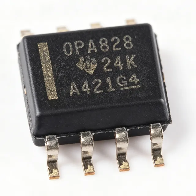
OPA828 - 45MHz 36V JFET Op Amp, 4nV Noise | TI
OPA828

OPA828 - 45MHz 36V JFET Op Amp, 4nV Noise | TI

The Texas Instruments OPA828 is a high-speed JFET-input operational amplifier delivering 45 MHz gain bandwidth product, 150 V/us slew rate, and 36 V operation with rail-to-rail output (RRO) in SOIC-8 and HVSSOP-8 (DGN) packages. It is the next-generation successor to the industry-standard OPA627 and OPA827, combining high speed with high DC precision. A JFET-input operational amplifier is a linear amplifier IC whose input stage uses junction field-effect transistors, giving it extremely low input bias current (picoampere level) while preserving the voltage-noise performance of a bipolar front end. Within the power management and signal-chain hierarchy, op amps form the core of analog signal conditioning between sensors and data converters. Key features include 4 nV/Hz input voltage noise density at 1 kHz, only 60 nVRMS of noise from 0.1 Hz to 10 Hz, 50 uV input offset voltage, and 0.45 uV/C offset drift. JFET inputs draw just 1 pA typical bias current, and MUX-friendly inputs simplify multiplexed signal chains. The wide supply range of +/-4 V and above supports 36 V single-supply operation. Architecturally, the OPA828 pairs a precision JFET input stage with a rail-to-rail output stage, enabling maximum output swing into ADCs and loads on low supply rails. Compared with the OPA627, TI documents wider bandwidth, higher slew rate, and rail-to-rail output as the key upgrade paths (per the TI comparison tool). Typical applications include photodiode transimpedance amplifiers, precision ADC driver front ends, high-fidelity audio stages, and test-and-measurement signal conditioning where low bias current, low noise, and high speed must coexist. Design consideration: ensure headroom for the JFET common-mode input range, and decouple supply pins with 0.1 uF ceramics placed within 2 mm; for TIA use, compensate feedback capacitance against input capacitance to preserve phase margin.

RFQ צור קשר
OPA828IDR - 45MHz JFET Op Amp, 4nV/√Hz | TI | Precision Amplifier
OPA828IDR

OPA828IDR - 45MHz JFET Op Amp, 4nV/√Hz | TI | Precision Amplifier

The Texas Instruments OPA828IDR is a high-speed, JFET-input operational amplifier delivering 45 MHz gain bandwidth, 150 V/us slew rate, and 4 nV/√Hz voltage noise in an 8-pin SOIC package. It operates over a wide supply range of ±4 V to ±18 V (36 V total) with rail-to-rail output (RRO), positioning it as the next-generation successor to the legendary OPA627 and OPA827 op amps. A JFET-input operational amplifier is a type of precision amplifier whose input stage uses junction field-effect transistors, providing extremely low input bias current (picoampere range) and high input impedance. Within the signal-chain hierarchy, op amps sit between sensors and data converters, serving as the general-purpose analog building block for amplification, filtering, buffering, and transimpedance conversion. Key features include 50 uV input offset voltage, 0.45 uV/C offset drift, 1 pA typical input bias current, and only 60 nVRMS of noise from 0.1 Hz to 10 Hz. These DC precision specifications make the OPA828 suitable for applications where both speed and accuracy are demanded simultaneously - a rare combination. MUX-friendly inputs allow multiplexed signal chains without settling artifacts or charge-injection damage. Architecturally, the OPA828 pairs a JFET input stage with a rail-to-rail output stage, combining classic precision topology with modern output swing. The RRO output maximizes dynamic range in low-voltage systems while the 36 V supply rating supports traditional ±15 V industrial analog rails without redesign. Typical applications include photodiode transimpedance amplifiers (TIA), high-fidelity audio front ends, precision ADC and DAC buffer stages, and active filters in test and measurement instrumentation. The wide 36 V supply range is particularly valuable for industrial designs retaining legacy ±15 V rails. For design, ensure supply decoupling with 0.1 uF ceramic capacitors placed within 3 mm of each supply pin. When replacing an OPA627, verify compensation and bias-current paths, as community feedback shows some legacy TIA circuits require adjustment despite pin compatibility. This page synthesizes distributor pricing, drop-in alternatives, and practical design notes not found in the manufacturer datasheet.

USD $1.75 צור קשר
OPA842ID - 400 MHz Low-Distortion Op Amp | Texas Instruments
OPA842ID

OPA842ID - 400 MHz Low-Distortion Op Amp | Texas Instruments

Texas Instruments OPA842ID is a wideband, low-distortion, unity-gain-stable voltage-feedback operational amplifier with a 400 MHz gain-bandwidth product, 400 V/us slew rate, and single-amplifier configuration in an 8-pin SOIC package. It operates from ±5 V to ±6 V and is specified for -40 °C to +85 °C ambient temperature operation. An operational amplifier is a high-gain differential amplifier used to amplify small input signals while imposing minimal distortion or unwanted noise. The OPA842 belongs to the voltage-feedback amplifier family within the broader operational-amplifier and signal-conditioning semiconductor hierarchy. Its unity-gain stability permits operation as a low-noise gain stage without requiring external compensation for a unity-gain configuration. The device uses a voltage-feedback architecture with two internal gain stages. According to the Texas Instruments OPA842 product information, this design provides a combination of high speed and dynamic range while maintaining low harmonic distortion across a wide frequency range. The 400 MHz gain-bandwidth product supports high-bandwidth signal processing, while the 400 V/us slew rate allows the amplifier to reproduce large-amplitude, rapidly changing signals with limited slew distortion. OPA842ID is suitable for test and measurement, communications, video, imaging, and general-purpose analog signal-chain applications. It can serve as a low-gain buffer, a wideband voltage amplifier, a driver for downstream circuitry, or an active element in analog filtering and feedback networks. Unity-gain stability is especially useful when the required closed-loop gain is close to 1. The principal design tradeoff is operating speed versus power dissipation and system noise. High-speed feedback loops require short, well-controlled PCB traces, stable power-supply bypassing, and careful termination of unused inputs. Follow the pin-description and typical-application tables in the manufacturer datasheet when assigning input bias, supply connections, output loads, and compensation values. This product page consolidates the verified device identity, package and operating details, application guidance, comparison parameters, and design considerations needed to evaluate OPA842ID before schematic capture or prototype assembly.

RFQ צור קשר
OPA843ID - 800 MHz Wideband Operational Amplifier | Texas Instruments
OPA843ID

OPA843ID - 800 MHz Wideband Operational Amplifier | Texas Instruments

The Texas Instruments OPA843ID is a single-circuit, wideband, low-distortion, medium-gain voltage-feedback operational amplifier with an 800 MHz gain-bandwidth product, 1000 V/us slew rate, and operation from a 10 V to 12 V supply in an 8-pin SOIC package. Designed for high-speed signal chains, it combines broad bandwidth with low distortion and is suitable for communications, test-and-measurement, video, and data-acquisition systems. A voltage-feedback operational amplifier is a feedback-controlled amplifier that uses the error at its inverting input to correct the output. The OPA843 belongs to the broader operational-amplifier hierarchy, which includes instrumentation amplifiers, buffer amplifiers, comparators, and other analog signal-conditioning ICs. Its medium closed-loop gain range and wide operating bandwidth make it particularly useful when a design needs accurate high-frequency amplification rather than only low-frequency precision. The primary performance characteristics include an 800 MHz gain-bandwidth product and a 1000 V/us slew rate. These figures allow the amplifier to preserve large-amplitude signals encountered in instrumentation and RF-adjacent signal chains. The device operates from 10 V to 12 V, giving designers sufficient headroom for wide-swing output stages while supporting a dual-supply implementation centered at zero volts. The specified operating-temperature range extends from -40 °C to +85 °C for industrial-temperature applications. OPA843ID is configured as a voltage-feedback amplifier rather than a current-feedback amplifier. This topology supports conventional resistive feedback networks and is familiar to engineers designing gain blocks, active filters, impedance drivers, and signal conditioners. Because the package is an 8-pin SOIC, PCB footprint reuse is straightforward when a new amplifier has the same supply arrangement, pin functions, and feedback topology. Pin assignments and support-network details should nevertheless be checked against the manufacturer datasheet before production release. Typical applications include broadband instrumentation, communications receivers, analog-to-digital converter input interfaces, active filters, pulse-shape circuits, and test equipment. In these applications, the 800 MHz bandwidth handles fast transitions while the 1000 V/us slew rate limits slew-related distortion. When driving cables, analog-to-digital converters, or other finite-impedance loads, the output-current capability and output-voltage swing should be checked against the actual load and supply conditions. The main design trade-off is supply and output-stage headroom. A 10 V to 12 V supply supports high output swing, but it is not interchangeable with a modern low-voltage, rail-to-rail amplifier. Decoupling capacitors, feedback resistor selection, source and load impedances, and stability conditions determine practical bandwidth. Use the manufacturer datasheet and its evaluated application circuits to select compensation and confirm performance across the required gain and frequency range. This page combines the verified manufacturer and distributor product information with engineering-focused comparisons, application guidance, package details, and design notes. It highlights where the OPA843ID's bandwidth, slew rate, supply range, and low-distortion voltage-feedback architecture are most useful, while also identifying the information that must be checked in the datasheet before a drop-in PCB or production design is approved.

RFQ צור קשר
OPA846ID - 1.75GHz Wideband Voltage-Feedback Op Amp | TI
OPA846ID

OPA846ID - 1.75GHz Wideband Voltage-Feedback Op Amp | TI

Texas Instruments OPA846ID is a wideband, low-noise voltage-feedback operational amplifier with 1.75 GHz gain-bandwidth product, approximately 400 MHz bandwidth, and 625 V/us slew rate. The device is supplied in an 8-pin SOIC package and consumes 12.6 mA of supply current. Its combination of high speed, low input voltage noise, and strong large-signal performance makes it suitable for signal conditioning, active filtering, data acquisition, communications, and high-frequency instrumentation. A voltage-feedback operational amplifier is a gain-control device whose closed-loop bandwidth depends primarily on the noise gain selected by the feedback network. Unlike a current-feedback amplifier, a voltage-feedback amplifier maintains a defined gain relationship through its inverting and non-inverting inputs. The OPA846 combines this familiar topology with very high gain-bandwidth product and large-signal output drive, placing it within the high-speed analog amplifier category of the broader semiconductor and signal-processing hierarchy. The principal features of the OPA846ID include a 1.75 GHz gain-bandwidth product, approximately 400 MHz amplifier bandwidth, 625 V/us slew rate, and low 12.6 mA supply current. The low-noise architecture is suitable for systems in which the amplifier must preserve small signals while operating at high frequencies. Its low distortion and high output-drive capability also make it more useful than a general-purpose precision op amp in video, communications, and instrumentation signal paths. Internally, the OPA846 uses a classical differential input stage, two stages of forward gain, and a high-power output stage. This architecture combines low input-voltage noise with high bandwidth and large-signal performance. The differential stage provides the low-noise input behavior, the forward-gain stages establish the high gain-bandwidth product, and the output stage supplies the current needed to drive downstream circuits while maintaining low distortion. The manufacturer identifies the device as a single-circuit, voltage-feedback amplifier. Typical applications include wideband active filters, video-signal conditioning, ultrasound and medical instrumentation, communications receivers, test-equipment front ends, and clock or data-processing interfaces. In these applications, the 1.75 GHz gain-bandwidth product supports operation at high closed-loop gains when the feedback network is designed carefully. The 625 V/us slew rate allows the output to track large-amplitude, high-frequency signals, while low noise helps preserve weak signals ahead of later amplification or conversion stages. Designers should account for the bandwidth and stability consequences of the selected gain. The feedback resistors and compensation network determine the effective noise gain, and parasitic capacitance around the high-speed amplifier can alter stability. Short feedback paths, careful grounding, controlled impedance routing, and clean supply decoupling are particularly important at the bandwidth levels supported by this device. Component selection must also preserve adequate phase margin at the intended closed-loop gain and signal amplitude. OPA846ID is ordered in an 8-pin SOIC package with an operating temperature range of -40°C to +85°C. This page combines manufacturer specifications, sourcing information, drop-in candidate review, comparison data, and practical high-speed layout guidance to support component selection and board-level implementation.

RFQ צור קשר
OPA858QIDSGRQ1 - 5.5GHz FET-Input TIA Op-Amp Q1 | TI
OPA858QIDSGRQ1

OPA858QIDSGRQ1 - 5.5GHz FET-Input TIA Op-Amp Q1 | TI

The Texas Instruments OPA858QIDSGRQ1 is an automotive-qualified (AEC-Q100), wideband, low-noise decompensated operational amplifier with FET (CMOS) inputs, delivering a 5.5-GHz gain bandwidth product (GBWP) while remaining stable at a minimum gain of 7 V/V. It is supplied in a compact 8-pin WSON (2x2 mm) surface-mount package. A decompensated amplifier is an operational amplifier internally compensated for stable operation only above a minimum closed-loop gain (here 7 V/V). By removing the compensation for unity-gain stability, the decompensated topology achieves dramatically higher bandwidth and lower input-referred noise than unity-gain-stable amplifiers of comparable process technology. In the signal-chain hierarchy, the OPA858-Q1 sits as a wideband voltage-feedback amplifier serving transimpedance amplifier (TIA) and high-gain voltage amplifier roles in high-speed analog front ends. Key features include the 5.5-GHz GBWP that enables high closed-loop bandwidths at transimpedance gains in the range of tens to hundreds of kilo-ohms, FET inputs that minimize input bias current effects on photodiode and high-impedance nodes, and single-ended single-channel configuration optimized for high-speed signal paths. The Q1 variant is manufactured on TI automotive flows and is qualified per AEC-Q100, supporting automotive lidar, imaging, and test applications that demand supply-chain traceability and automotive-grade reliability. The architecture combines CMOS input devices with wideband voltage-feedback internals, yielding low input capacitance that is critical in TIA designs because photodiode plus amplifier input capacitance directly limits achievable bandwidth per unit of transimpedance gain. TI provides the OPA858 together with a companion evaluation module and application collateral covering feedback resistor selection, compensation capacitor sizing, and stability analysis. Typical applications include automotive lidar receiver TIAs, wideband photodiode amplification in optical sensing, high-speed voltage amplification stages, and wideband test and measurement front ends. The device suits any signal chain that requires gain of 7 V/V or higher with multi-hundred-megahertz to gigahertz-class bandwidth. Design consideration: because the amplifier is only stable at gain >= 7 V/V, noise-gain analysis must be performed at all frequencies, including input capacitance effects at the inverting node; verify phase margin with the TI datasheet stability curves before finalizing feedback-network values.

RFQ צור קשר
OPA860ID - 370MHz Wide-Bandwidth OTA & Buffer | Texas Instruments
OPA860ID

OPA860ID - 370MHz Wide-Bandwidth OTA & Buffer | Texas Instruments

The Texas Instruments OPA860ID is a single-channel, wide-bandwidth operational transconductance amplifier and voltage buffer packaged in an 8-pin SOIC. It combines a bipolar operational transconductance amplifier (OTA) with a unity-gain buffer output, providing a 370 MHz bandwidth and approximately -4.2 V to +4.2 V output swing on a single +5 V supply. An operational transconductance amplifier is an amplifier whose output current is controlled by an input voltage. In signal-path terms, an OTA belongs to the operational-amplifier family, but it transfers current rather than presenting a conventional voltage output. The OPA860ID also contains a wide-band voltage buffer that can follow the OTA output, giving designers both transconductance and buffered-voltage operating modes in one package. The principal feature of the OPA860ID is its 370 MHz small-signal bandwidth. This bandwidth supports high-speed video, RF, and intermediate-frequency signal chains where the transconductance stage must amplify small control or error signals without excessive delay. The OTA can also be used as a current-output stage, while the internal buffer supplies a low-impedance voltage output when the system requires conventional signal routing. Because the device combines an OTA and a buffer, the circuit designer can select the more appropriate output stage for a given application. The OTA section operates as a voltage-controlled current source, while the buffer section provides a conventional voltage output. This versatility is useful in video and RF systems that evaluate gain, impedance, and loading behavior during prototype development. Typical uses include high-performance video processing, RF and IF signal conditioning, current-feedback and transconductance-based filter stages, laboratory instrumentation, and wideband analog signal chains. The single +5 V supply arrangement simplifies system design compared with dual-supply analog circuits, although output headroom must remain within the approximately -4.2 V to +4.2 V swing limits. PCB layout should prioritize short, controlled-impedance traces at the high-impedance OTA input. Keep the signal and ground paths compact, place bypassing capacitors close to the supply pins, and avoid long traces adjacent to switching nodes. These layout practices limit parasitic capacitance, reduce unintended feedback, and preserve the wideband behavior that distinguishes the OPA860 from ordinary low-frequency operational amplifiers. This page organizes the OPA860ID electrical characteristics, package information, application guidance, and verified alternatives into a design-focused reference. It also compares the available orderable family members so engineers can assess drop-in reuse while accounting for supply configuration, output-current capability, bandwidth, and package differences.

RFQ צור קשר
OPA861ID - 80 MHz Wide-Bandwidth OTA | Texas Instruments
OPA861ID

OPA861ID - 80 MHz Wide-Bandwidth OTA | Texas Instruments

The Texas Instruments OPA861ID is a wide-bandwidth operational transconductance amplifier (OTA) with an 80 MHz characteristic bandwidth, packaged in an 8-pin SOIC. It is a bipolar analog IC intended for signal-processing circuits that require voltage-to-current conversion rather than conventional voltage-output operational-amplifier behavior. The OPA861ID is associated with high-performance video, RF, and IF signal chains, where a transconductance element can provide controlled current drive, programmable gain, and analog signal conditioning. An operational transconductance amplifier is a voltage-controlled current-source building block. Its differential input voltage is converted into an output current that is proportional to the input and determined by the transconductance gain. In the OPA861 family, the manufacturer describes the device as a versatile monolithic wideband bipolar OTA. The OTA is therefore positioned above basic passive and discrete signal-conditioning components in the hierarchy of analog signal-processing ICs, while remaining a specialized alternative to a conventional operational amplifier. The key headline characteristics of the OPA861ID are its 80 MHz bandwidth designation, bipolar implementation, wide-bandwidth transconductance operation, and 8-pin SOIC package. These attributes make the device suitable for wideband analog systems in which signal bandwidth and controlled current output are more important than the familiar voltage-output architecture of an ordinary op amp. The 8-SOIC format also supports conventional surface-mount PCB assembly and routing, although the exact footprint dimensions and exposed-pad details should be checked against the package drawing. OPA861ID applications include RF and intermediate-frequency signal conditioning, high-performance video circuits, current-feedback filtering, analog gain-control paths, and instrumentation requiring a voltage-to-current conversion stage. In an RF or IF chain, the OTA can operate within a feedback loop that establishes filtering or gain, allowing the amplifier's transconductance behavior to be used as an active analog building block. In video systems, the wide-bandwidth characteristic supports higher-frequency signal paths than a general-purpose precision op amp. Designers should treat the OPA861ID as a high-speed analog device rather than a generic voltage regulator or precision low-noise amplifier. Input and feedback component selection, signal amplitude, supply headroom, and output-current limits must be evaluated together. The OPA861ID datasheet and its OTA section should be used to establish the exact recommended operating conditions, compensation approach, and application-circuit topology.

RFQ צור קשר
OPA875ID - 700 MHz 2:1 Video Multiplexer | Texas Instruments
OPA875ID

OPA875ID - 700 MHz 2:1 Video Multiplexer | Texas Instruments

The Texas Instruments OPA875ID is a single-channel, 700 MHz video multiplexer with an integrated +2 gain amplifier, supplied in an 8-pin SOIC package. It combines two high-speed video inputs with one output, consumes only 11 mA, and provides greater than 425 MHz large-signal bandwidth with a 4 VPP signal. The OPA875ID is therefore suited to wideband video routing where compactness, low power consumption, and short signal paths are important. A high-speed video multiplexer is a signal-routing device that selects one of multiple analog inputs and presents that selected signal at a common output. The OPA875ID belongs to the broader video-switch IC and high-speed analog multiplexer categories. Unlike a general-purpose analog switch that merely connects a source to a load, it integrates a +2 video-amplifier channel and optimized input switching, allowing it to drive downstream video equipment while preserving wideband signal integrity. Principal features include a 700 MHz device bandwidth, greater than 425 MHz large-signal bandwidth at 4 VPP, +2 gain, and a single-channel 2:1 configuration. Its 11 mA supply-current consumption reduces the power burden in distributed video systems. The manufacturer's product information also indicates improved gain accuracy and switching glitch compared with earlier multiplexer solutions, using a new input-stage switching approach. The OPA875ID is available in SO-8 and small MSOP-8 package options, with OPA875ID identifying the SO-8 ordering variant. The manufacturer describes the OPA875 as a very wideband multiplexer suitable for high-speed video systems. Its architecture is intended to minimize the number of external signal-conditioning stages required in moderate-bandwidth routing applications while maintaining a compact footprint. Typical uses include professional video routing, broadcast and monitoring equipment, test and measurement systems, and other applications that route baseband or composite-style high-speed video signals. The integrated +2 gain can reduce the need for a separate gain stage, while the two-input multiplexer consolidates source selection into a single device. Systems requiring three multiplexed channels should evaluate the manufacturer's OPA3875 family instead. The primary design consideration is signal integrity: routing boards must use controlled-impedance traces, short connections, solid ground references, and careful termination around the high-speed amplifier inputs and output. Supply decoupling should follow the manufacturer's recommended layout, and unused or configuration pins must be connected exactly as specified in the datasheet. This page consolidates manufacturer specifications, distributor availability references, package details, application guidance, and design considerations. It also distinguishes verified OPA875 ordering variants from packaging-only options, helping engineers avoid treating reel codes or different-package versions as true pin-compatible drop-in replacements.

RFQ צור קשר
OPA890ID - 130MHz, 500V/us Single Op Amp | Texas Instruments
OPA890ID

OPA890ID - 130MHz, 500V/us Single Op Amp | Texas Instruments

Texas Instruments OPA890ID is a low-power, wideband, single voltage-feedback operational amplifier with a disable function, one amplifier per package, a 130 MHz gain-bandwidth product, and a 500 V/us slew rate. Designed for low-voltage operation, the device accepts supply voltages from ±1.5 V to ±6 V and is offered in an 8-pin SOIC package. A voltage-feedback operational amplifier is an analog signal-conditioning amplifier that uses negative feedback to control gain and bandwidth. The OPA890ID belongs to the operational-amplifier hierarchy and is suitable for precision analog, communications, instrumentation, and signal-processing systems requiring much greater bandwidth than general-purpose amplifiers. Key characteristics include a 130 MHz gain-bandwidth product, 500 V/us slew rate, single-amplifier configuration, and an operating supply range of ±1.5 V to ±6 V. The wide bandwidth enables closed-loop operation at high frequencies, while the high slew rate supports accurate reproduction of rapidly changing waveforms. The shutdown function allows the amplifier to be disabled when a circuit does not require continuous operation. The OPA890ID uses a voltage-feedback architecture, which provides a direct relationship between input differential voltage and output voltage through the external feedback network. Its bandwidth and slew-rate characteristics make it appropriate for low-amplitude, high-speed signal paths rather than slow precision-only applications. Designers must account for gain-bandwidth interaction, output-voltage swing, input common-mode range, stability, and the effect of parasitic capacitance at high frequencies. Typical uses include video and communications signal conditioning, waveform generation, data-conversion interfaces, active filters, and low-level instrumentation. The disable pin can support power management or isolate an amplifier during selected operating modes. In dual-supply systems, the ±1.5 V to ±6 V capability permits operation from low-rail analog and mixed-signal supplies. PCB implementation should minimize trace length around the feedback network, maintain symmetrical routing, provide a solid ground reference, and place decoupling capacitors close to the supply pins. Feedback-component values should be checked against the selected closed-loop gain and the device's stability requirements. This page combines ordering information, verified electrical details, comparison guidance, and practical high-frequency layout considerations.

RFQ צור קשר
OR2T40A6PS240-DB - ORCA 2 FPGA, 3600 Cells, 240-BFQFP | Lattice
OR2T40A6PS240-DB

OR2T40A6PS240-DB - ORCA 2 FPGA, 3600 Cells, 240-BFQFP | Lattice

The Lattice Semiconductor OR2T40A6PS240-DB is an ORCA Series 2 Field-Programmable Gate Array (FPGA) IC with 3,600 logic cells, 57,600 usable gates, 184 user I/Os, and a maximum internal operating frequency of 294.12 MHz, packaged in a 240-pin Square Flat Pack (BFQFP with exposed pad) also referred to as SQFP2-240 / PQFP240. The device is fabricated on a 0.3 µm CMOS process and operates from a 3.3 V supply, providing a logic density and I/O count tuned to bus-oriented and telecom-style glue-logic designs of the late-1990s / early-2000s vintage. A field-programmable gate array (FPGA) is a type of programmable logic device that combines an array of configurable logic blocks (CLBs), programmable interconnects, and programmable I/O cells around a central SRAM or antifuse configuration memory, allowing digital designers to implement custom logic without manufacturing a custom ASIC. Within the broader taxonomy, an FPGA sits below the Programmable Logic Device (PLD) superfamily and above fixed-function ASICs, while being a sibling of CPLDs (Complex PLDs) - the difference being that FPGAs use finer-grained logic elements distributed across a wider interconnect fabric. The ORCA 2 family is Lattice's second-generation SRAM-based FPGA, predating the migration to ispXPGA / LatticeECP / ECP2/3/4/5 modern families. Key features include 900 Configurable Logic Blocks (CLBs), 240-pin BFQFP exposed-pad package with gull-wing leads, 0.3 µm CMOS technology, 3.3 V core/IO supply, 184 maximum user I/Os, 3600 logic cells, and a Die Revision -DB variant. The "OR2T40A6" prefix encodes the family (ORCA 2), the cell count (T40 ≈ 3,600 cells), the speed grade (-6), the voltage (3.3 V), and the package designator (PS240 = Power-SQFP 240 pins). The "-DB" suffix is a special die-revision / quality mark used for Lattice distributor-channel stock. The OR2T40A6 architecture uses SRAM-based configuration memory distributed throughout the die, allowing unlimited reconfiguration, in-system programming through JTAG, and ISE-style tool flows. The rich interconnect fabric and block-RAM/PLL resources of this generation made the part suitable for ASIC prototyping, custom bus bridges, and DSP pre-processing pipelines. The 294.12 MHz system clock target confirms high-speed datapath capability for the era. Typical applications include telecom interface glue logic, bus bridges and protocol converters (e.g., PCI to local bus, Utopia to SPI), ASIC prototyping and emulation platforms, embedded controller cores, and industrial automation controllers. The 184 available I/Os make the part well-suited to bus-heavy designs that need to aggregate multiple peripheral interfaces. When designing with this device, ensure that the 3.3 V supply is well decoupled (at least 0.1 µF ceramic plus a bulk tantalum or polymer) within 1 cm of each power pin and that the exposed-pad is soldered to a contiguous ground copper pour. Configuration loading through JTAG or Slave Serial mode should follow Lattice's ORCA Series 2 programming reference manual. This page synthesizes distributor pricing, drop-in alternatives (OR2T40A7PS240-DB speed-grade upgrade and OR2T40A6PS240I-DB industrial-temp variant), and practical design notes not found in the standalone datasheet.

RFQ צור קשר
OSD3358-512M-BAS - AM3358 SiP 1GHz Cortex-A8 512MB DDR3 | Octavo Systems
OSD3358-512M-BAS

OSD3358-512M-BAS - AM3358 SiP 1GHz Cortex-A8 512MB DDR3 | Octavo Systems

The Octavo Systems OSD3358-512M-BAS is a System-in-Package (SiP) module that integrates the Texas Instruments AM3358 ARM Cortex-A8 application processor with 512 MB of DDR3 SDRAM and all required power management circuitry into a single 400-ball BGA package measuring approximately 20 mm x 20 mm. The integrated AM3358 silicon runs at up to 1 GHz and exposes the standard ARM Cortex-A8 NEON SIMD engine for multimedia and signal processing workloads, while the on-package DDR3 memory delivers low-latency access critical for deterministic Linux real-time behavior. A System-in-Package is an advanced packaging technology that combines multiple discrete silicon dies - in this case the AM3358 SoC, a DDR3 memory die, and a TPS65217C power management IC die - into one BGA substrate, eliminating the complex PCB layout, signal integrity work, and discrete component sourcing required when these parts are used individually. The OSD335x family sits within the broader System-on-Module (SoM) hierarchy, providing pre-validated multi-die integration so design effort can focus on application peripherals rather than core compute hardware bring-up. Key differentiating features include the 400-ball BGA that is a superset of the TI AM3358 ZCZ 18x18 BGA footprint - meaning most signals are pin-compatible with the discrete AM3358 - plus integrated 512 MB DDR3, on-die power sequencing, and Octavo's documented pin assignment guidance (App Note 1002) for migrating from the TI AM3358 reference design. The SiP eliminates eight discrete power rails, six decoupling networks, and the DDR3 PCB fly-by routing that normally dominates AM3358 designs. Architecturally, the OSD3358 wraps the AM3358's Cortex-A8 superscalar core, SGX530 graphics accelerator, dual PRU-ICSS industrial communication subsystems, two Gigabit-capable Ethernet MACs, and three USB ports, exposing them through Octavo's documented BGA pin map. The package dimensions are larger than the bare AM3358 but still fit inside a 28 mm x 28 mm PCB footprint, suitable for compact industrial, robotics, and IoT gateway designs. Typical applications include the BeagleBone Blue robotics platform, industrial IoT gateways, building automation controllers, human-machine interface (HMI) panels, and Linux-based data acquisition systems. The integrated power management and DDR3 simplify UL/CE/FCC certification because designers only qualify the host PCB rather than a high-speed memory interface. A primary design consideration: although the OSD3358 is pin-compatible with the bare AM3358 ZCZ at the signal level, the 20 x 20 BGA is mechanically larger, and any DDR3 routing already done for the AM3358 must be discarded. Designers migrating should consult Octavo App Note 1002 for the exact signal-to-ball mapping differences. This page synthesizes distributor pricing, drop-in alternative SKUs, and migration notes from App Note 1002 that are not present in the bare AM3358 datasheet, giving engineers a single reference for procurement and design-in.

RFQ צור קשר
OSD3358-512M-BAS-XB - SiP ARM Cortex-A8 1GHz | Octavo Systems
OSD3358-512M-BAS-XB

OSD3358-512M-BAS-XB - SiP ARM Cortex-A8 1GHz | Octavo Systems

The Octavo Systems OSD3358-512M-BAS-XB is a System-In-Package (SiP) that integrates a Texas Instruments Sitara AM3358 ARM Cortex-A8 processor clocked up to 1 GHz, 512 MB of DDR3 SDRAM, a TPS65217C power management IC, and passives into a 400-ball BGA package. The XB industrial-temperature variant extends the operating range from 0 C to +85 C offered by the BAS commercial variant to -40 C to +85 C, enabling ruggedized deployments in factory-floor and outdoor equipment. An SiP (System-In-Package) is a single BGA module that integrates the processor, memory, and power management into one substrate. Compared to a discrete SoC + external DDR3 + discrete PMIC layout, an SiP eliminates high-speed DDR3 routing between chips, reduces PCB layer count, simplifies DDR3 tuning, and shortens EMC qualification. In the OSD335x taxonomy, the device belongs to the AM3358-based Octavo Systems SiP family that brings a Sitara Application Processor into a single BGA footprint suitable for industrial SBCs, gateways, and HMI designs. Key features include an ARM Cortex-A8 core with NEON SIMD, a SGX530 graphics accelerator for display/HMI workloads, dual 32-bit LPDDR1/DDR2/DDR3 memory controller (DDR3 is internally populated to 512 MB), two industrial-grade PRU-ICSS subsystems for deterministic real-time I/O, three I2C, two SPI, two CAN, gigabit Ethernet, and integrated USB 2.0 high-speed PHYs. The TPS65217C handles all six supply rails (VDD_MPU, VDD_CORE, VDSPLL, VDDA1V8, VDDS, DDR3 VTT) and supports dynamic voltage scaling for energy-aware operation. The architecture reduces board area by approximately 60% relative to a discrete AM3358 design, accelerates time-to-market by removing DDR3 length-matching iterations, and simplifies EMI/ESD certification because high-speed nets are encapsulated inside the SiP substrate. Industrial users leverage the -40 C to +85 C rating for outdoor enclosures and factory automation, while still drawing on the full Sitara Linux and TI Processor SDK software ecosystem. Typical applications include industrial IoT gateways, programmable logic controllers, HMI panels, robotics controllers, edge vision nodes, and home/small-business networking appliances. The BeagleBone Blue robotics platform uses the BAS variant, demonstrating production-grade Linux system stability on this OSD3359/OCTAVO SiP family. For harsher-thermal environments, the -XB industrial-temperature variant is the preferred drop-in choice. When designing with the OSD3358-512M-BAS-XB, allow a minimum keep-out of 0.5 mm around the BGA and a 4-layer PCB with continuous GND beneath the package for thermal dissipation and DDR3 signal integrity. Use TI Processor SDK Linux or Debian images and consult the OSD335x reference schematic for proper PMIC sequencing and decoupling.

RFQ צור קשר
OSD3358-512M-BSM - ARM Cortex-A8 SiP, 1GHz, 512MB DDR3 | Octavo
OSD3358-512M-BSM

OSD3358-512M-BSM - ARM Cortex-A8 SiP, 1GHz, 512MB DDR3 | Octavo

The Octavo Systems OSD3358-512M-BSM is a System-in-Package (SiP) that integrates the Texas Instruments Sitara AM3358 ARM Cortex-A8 application processor with 512 MB of DDR3 memory, PMIC, and passives into a single 21x21 mm 256-ball BGA module. The SiP delivers up to 1 GHz Cortex-A8 performance with NEON SIMD and a PowerVR SGX530 graphics accelerator, exposing the full AM3358 peripheral set - 2x PRU-ICSS, USB 2.0, gigabit Ethernet, six controllers, and McASP - on a compact surface-mount footprint. According to the Octavo product page, this commercial temperature variant is purpose-built for design engineers who want to drop a complete compute subsystem onto a custom PCB without handling BGA DDR routing or PMIC placement. A System-in-Package combines multiple silicon dies and passive components inside a single BGA package, eliminating inter-chip PCB traces and reducing both board area and BOM count. SiPs are a category of multi-chip module (MCM) optimized for embedded compute; alternatives include chip-on-board (CoB) and discrete multi-chip layouts. By integrating the DDR3 interface inside the package, the OSD3358 removes the most challenging signal-integrity work - matched-length 16-bit memory bus - from the customer's PCB, letting teams focus on application logic. Key features of the OSD3358-512M-BSM include 512 MB of 32-bit wide DDR3 with on-package termination, an integrated TI TPS65217C PMIC and LDO stack, four UART, two I2C, two SPI, and dual gigabit-capable industrial Ethernet MACs. The exposed AM3358 peripherals include two independent PRU subsystems for real-time I/O, two USB 2.0 ports (one HS host, one HS dual-role), and the SGX530 3D graphics engine for HMI rendering at up to 1080p. With 512 MB of system RAM and full MMU virtualization, the module can run Debian Linux, FreeRTOS, or Android 4.x out of the box. Hardware-wise, the SiP uses 1.27-mm-pitch BGA pins to expose 256 signal balls on a 21x21 mm land pattern, with a top-side shielding can for EMI suppression. The pocketbeagle-compatible pin map (P1/P2 headers, 72 GPIOs) and reference schematics dramatically shorten prototyping. Octavo notes the device supports industrial I/O voltages via the on-package PMIC; a coin-cell backup rail and RTC are not integrated and require external implementation. Typical applications include industrial automation gateways, robotics motor controllers, building-automation edge nodes, retail kiosks with a graphical HMI, and battery-powered portable data loggers. The extended -25 C to +85 C variant (OSD3358-512M-BEM) covers harsher industrial deployments where the commercial BSM is marginal. The OSD3358-512M-BSM is also commonly used as a turnkey compute core for hand-held instruments and PoE-powered IP cameras. When designing with this SiP, engineers must treat the thermal pad and shielding can as a single thermal mass; a minimum 4-layer PCB with continuous ground pour is recommended to keep junction temperature within the AM3358's 90 C envelope. The on-package PMIC requires only a single 5 V rail - simplifying power-tree design - but the DDR3 self-refresh current and PRU real-time latency must be budgeted against battery life in portable designs. This page synthesizes XAIPART distributor pricing, OSD335x-family drop-in alternatives, and curated design notes not collected on the Octavo product brief.

RFQ צור קשר
P1010NSE5FFA - QorIQ P1010 SoC 667 MHz e500v2 | NXP
P1010NSE5FFA

P1010NSE5FFA - QorIQ P1010 SoC 667 MHz e500v2 | NXP

The NXP (formerly Freescale) P1010NSE5FFA is a QorIQ P1010 communications processor built around a single PowerPC e500v2 core running at 667 MHz (industrial-grade speed grade), integrating SEC 4.4 security acceleration, DDR3/DDR3L memory controller, GbE, USB 2.0, SATA, PCIe, and trusted-boot logic in a 425-pin TEBGA-1 (19x19 mm) package. This particular part variant encodes the package, temperature grade, encryption, frequency, and revision indicators in its nomenclature, with the NSE suffix denoting the 667 MHz industrial grade, lead-free TEBGA-1 package. A communications processor (or SoC, system-on-chip) is a single integrated circuit that combines CPU cores, network/IO peripherals, memory interfaces, and security engines to serve as the central processing hub for embedded networking and industrial equipment. In the broader hierarchy, the P1010NSE5FFA belongs to QorIQ -> PowerQUICC III family -> Power Architecture networking SoCs -> communications processors. This taxonomy is important because QorIQ P1 devices target cost- and power-sensitive workloads downstream of higher-tier P2/P4 platforms. Key features include a 32-bit Power Architecture e500v2 core with double-precision FPU, dual GbE MACs, two PCIe Gen1 controllers, two SATA-II interfaces, USB 2.0 host/device, SPI, UART, I2C, SDHC, 16-bit DDR3/DDR3L controller with ECC, and SEC 4.4 hardware crypto accelerator supporting AES, 3DES, RSA, and elliptic curves. The trusted-boot engine, JTAG, and on-chip PLL complete the integrated BOM. Architecturally the device combines a book-E/e500v2 application core with platform glue that integrates most of the peripherals that previously required external ASICs - meaning a 667 MHz single-core SoC can replace a legacy PowerQUICC II + companion chip design, cutting PCB area and BOM. The 45 nm process and low core voltage keep TDP within typical industrial thermal envelopes. Typical applications include industrial Ethernet gateways, smart-grid/energy routers, secure IoT gateways, factory-floor protocol converters, networked printers, and small-form-factor industrial firewalls. The integrated SEC makes it particularly suited to VPN/secure tunneling with hardware offload. When designing with this part, follow the QorIQ reference-board layout for DDR3 trace matching, keep the analog power rails well decoupled, and confirm the exact pinctrl multiplexing against the Reference Manual since the 425-ball TEBGA-1 is dense and footprints are mechanically single-sourced. This page synthesizes distributor stock, same-family NXP drop-in variants, packaging-grade equivalents, and trusted-boot design notes unavailable on bare Digi-Key catalog listings.

RFQ צור קשר