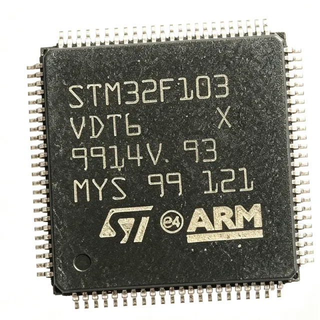
STM32F103VBI6
STM32F103VBI6 - 72MHz Cortex-M3 128KB MCU | STMicroelectronics
STMicroelectronics STM32F103VBI6 is an Arm Cortex-M3 32-bit microcontroller with a 72 MHz maximum CPU frequency, 128 KB of Flash memory, and a 100-UFBGA package measuring 7 x 7 mm. The device belongs to the STM32F1 mainstream performance line and supports operation from 2.5 V to 3.3 V according to the supplied distributor data. It is positioned for embedded control, communications, industrial automation, USB, and CAN-based designs that require dense peripheral integration in a compact surface-mount package.
A microcontroller is a programmable semiconductor that integrates a processor core, nonvolatile program memory, working memory, peripherals, and interface logic on one device. The STM32F103 series combines an Arm Cortex-M3 core with dedicated timers, analog converters, communication interfaces, and general-purpose I/O. Within the product hierarchy, the STM32F103VBI6 is an Arm Cortex-M3 MCU, an embedded microcontroller, and a semiconductor designed for real-time embedded-control applications.
Verified product features include a 72 MHz CPU, 128 KB of Flash, seven timers, two ADCs, nine communication interfaces, USB support, and CAN support. Its 100-pin UFBGA package allows access to a large pin count without the lead span of a conventional 100-pin through-hole or LQFP package. The 7 x 7 mm land pattern is intended for high-density PCB layouts, but exposed-pad routing, assembly capability, and thermal performance must be evaluated against the complete manufacturer documentation.
The STM32F103VBI6 uses the Arm Cortex-M3 architecture with a 32-bit instruction set. Its 128 KB Flash provides on-chip program storage, while the peripheral mix supports common embedded-control tasks such as digital I/O, timing, analog measurement, serial communications, USB, and CAN. Exact SRAM capacity, ADC resolution, I/O voltage limits, timer channels, and electrical characteristics are not present in the supplied search data and therefore remain [DATA_NEEDED: SRAM capacity], [DATA_NEEDED: ADC resolution], and [DATA_NEEDED: detailed electrical characteristics].
Typical uses include industrial controllers, USB-connected embedded products, CAN network nodes, data-acquisition equipment, motor-control subsystems, and compact control boards. The seven timers and two ADCs make it relevant to systems combining periodic control functions with analog input conditioning. USB and CAN connectivity can reduce external interface hardware when the board already uses the STM32F1 ecosystem, although firmware, clocking, peripheral-equivalence, and qualification checks remain essential before redesigning an existing product.
The principal design consideration is that the 100-UFBGA package demands fine-pitch PCB layout and careful assembly planning. A manufacturer-qualified pin map was not included in the supplied data, so engineers must verify all 100 terminals, exposed-pad requirements, recommended decoupling, and test-point access in the official STM32F103 documentation before schematic capture or PCB release. Pricing also was not exposed in the supplied results, making procurement cost and lifecycle planning dependent on a current distributor quotation.
This product record consolidates the verified STM32F103VBI6 specifications, distributor availability, package information, interface features, sourcing links, and engineering caveats into one decision aid. It distinguishes documented facts from missing parameters and avoids presenting functional MCU alternatives as verified drop-in replacements, which is important because package, pin mapping, clock configuration, and peripheral compatibility must be confirmed independently.
RFQ
צור קשר