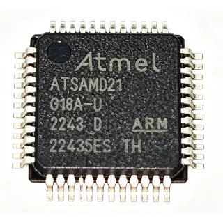
DSPIC33CH512MP205T-I/PT - Dual-Core DSC 512KB Flash TQFP-48 | Microchip
MPN: DSPIC33CH512MP205T-I/PT ✓ פעילDSPIC33CH512MP205T-I/PT סקירה
A DSC (Digital Signal Controller) is a hybrid device that merges the deterministic real-time control of a microcontroller with the computational throughput of a Digital Signal Processor (DSP). In the broader taxonomy, a DSC sits between an MCU and a DSP, supporting single-cycle MAC instructions and saturating arithmetic, while retaining on-chip peripherals such as ADCs, PWMs, and communication interfaces. The dsPIC33CH sub-family further extends this concept by integrating two cores on one die - allowing concurrent closed-loop control and high-level supervisory tasks within a single chip.
Key features of this device include dual independent cores with separate debugging ports, 12-bit ADC with up to 3.5 MSPS throughput, high-resolution PWM with 250 ps resolution for precision power conversion, CAN FD and multiple UART/SPI/I2C interfaces, and Functional Safety (FuSa) features for IEC 60730-class applications. The 48-pin TQFP package supports an industrial operating temperature range of -40C to +85C and is powered from 3.0 V to 3.6 V.
The architecture combines a 16-bit modified Harvard bus with DSP-specific accumulators and barrel shifters, achieving deterministic interrupt latency under 10 cycles. The master core handles communications and main control loops, while the slave core can execute time-critical DSP tasks such as field-oriented motor control or digital power conversion without contending with system software. This partitioning shortens firmware development cycles and enables modular certification strategies for safety-critical designs.
Typical applications include field-oriented control (FOC) motor drives, digital switched-mode power supplies, solar inverters, EV chargers, and industrial PLCs. The wide peripheral integration reduces external component count, making it a strong fit for compact motor-control and power-conversion boards where PCB area is at a premium.
When designing with this device, ensure that the master and slave core debug headers are correctly assigned and that the dedicated VDD/VSS pins for each ADC are properly decoupled. A 100 nF plus 10 uF capacitor stack placed within 5 mm of the AVDD pins is required to meet ADC SNR specifications.
This page synthesizes distributor pricing, drop-in same-family alternatives, parametric comparisons, and practical decoupling/thermal design notes not found in the manufacturer datasheet, giving engineers a single decision-ready view of the DSPIC33CH512MP205T-I/PT for control and DSP applications.
חלופות תחליף ישיר עבור DSPIC33CH512MP205T-I/PT — אותו מארז, תואם פין-לפין. חלקים במארז שונה הדורשים עיבוד מחדש של ה-PCB אינם נכללים.
וריאנטים בסדרה זו
דגמים מאותה סדרה התואמים Drop-in עם DSPIC33CH512MP205T-I/PT (אותו גורם צורה וטביעת רגל) — שונים ב Slave Core Speed, Package, ADC, Core Architecture, Operating Temperature.
DSPIC33CH512MP205-I/PT
✅ Drop-Inצור קשר לקבלת מחיר
הצג גיליון נתונים ←DSPIC33CH256MP205T-I/PT
✅ Drop-Inצור קשר לקבלת מחיר
הצג גיליון נתונים ←DSPIC33CH128MP205T-I/PT
✅ Drop-In📋 חלופה להתייחסות (לא בקטלוג)
DSPIC33CH256MP208-I/PT
✅ Drop-Inצור קשר לקבלת מחיר
הצג גיליון נתונים ←DSPIC33CH256MP206T-I/PT
✅ Drop-In📋 חלופה להתייחסות (לא בקטלוג)
DSPIC33CH256MP206-E/PT
✅ Drop-Inצור קשר לקבלת מחיר
הצג גיליון נתונים ←DSPIC33CH512MP205T-I/PT דירוגים מרביים ומאפיינים חשמליים
| Core Architecture | dsPIC33CH dual-core (master + slave) |
| Master Core Speed | 200 MHz / 100 MIPS |
| Slave Core Speed | 180 MHz / 90 MIPS |
| Program Flash | 512 KB |
| RAM | 48 KB |
| Slave PRAM | 4 KB |
| מתח אספקה | 3.0 V to 3.6 V |
| טמפרטורת פעולה | -40C to +85C |
| מארז | 48-pin TQFP (7x7 mm) |
| סוג הרכבה | Surface Mount |
| ADC | 12-bit, up to 3.5 MSPS |
| PWM Resolution | 250 ps high-resolution PWM |
| Communication | CAN FD, UART, SPI, I2C |
| Functional Safety | Yes (FuSa, IEC 60730 capable) |
| סטטוס RoHS | Compliant |
תצורת פינים של DSPIC33CH512MP205T-I/PT
| פין 1 | SDA1/RP58/RF0 — I2C1 SDA / remappable peripheral |
| פין 2 | SCL1/RP59/RF1 — I2C1 SCL / remappable peripheral |
| פין 3 | AN18/RP60/RF2 — Analogue input 18 / remappable peripheral |
| פין 4 | AN19/RP61/RF3 — Analogue input 19 / remappable peripheral |
| פין 5 | AVDD — Analogue supply voltage |
| פין 6 | AVSS — Analogue ground |
| פין 7 | AN20/RP62/RF4 — Analogue input 20 / remappable peripheral |
| פין 8 | AN21/RP63/RF5 — Analogue input 21 / remappable peripheral |
| פין 9 | VDD — Digital supply voltage |
| פין 10 | VSS — Digital ground |
| פין 11 | OSC1/CLKI/RC12 — Crystal oscillator input / external clock |
| פין 12 | OSC2/CLKO/RC15 — Crystal oscillator output |
| פין 13 | PGEC1/RP38/RB6 — Master-core ICSP clock |
| פין 14 | PGED1/RP39/RB7 — Master-core ICSP data |
| פין 15 | PGEC2/RP40/RB8 — Slave-core ICSP clock |
| פין 16 | PGED2/RP41/RB9 — Slave-core ICSP data |
| פין 17 | RE0 — I/O port E0 / remappable peripheral |
| פין 18 | RE1 — I/O port E1 / remappable peripheral |
| פין 19 | RE2 — I/O port E2 / remappable peripheral |
| פין 20 | RE3 — I/O port E3 / remappable peripheral |
| פין 21 | VDD — Digital supply voltage |
| פין 22 | VSS — Digital ground |
| פין 23 | RP42/RB10 — Remappable peripheral / PWM |
| פין 24 | RP43/RB11 — Remappable peripheral / PWM |
| פין 25 | RP44/RB12 — Remappable peripheral / PWM |
| פין 26 | RP45/RB13 — Remappable peripheral / PWM |
| פין 27 | RP46/RB14 — Remappable peripheral / PWM |
| פין 28 | RP47/RB15 — Remappable peripheral / PWM |
| פין 29 | S1MCLR/RE4 — Slave-core master clear / reset |
| פין 30 | MCLR/RE5 — Master-core master clear / reset |
| פין 31 | AN0/RP48/RC0 — Analogue input 0 / remappable peripheral |
| פין 32 | AN1/RP49/RC1 — Analogue input 1 / remappable peripheral |
| פין 33 | AN2/RP50/RC2 — Analogue input 2 / remappable peripheral |
| פין 34 | AN3/RP51/RC3 — Analogue input 3 / remappable peripheral |
| פין 35 | AN4/RP52/RC4 — Analogue input 4 / remappable peripheral |
| פין 36 | AN5/RP53/RC5 — Analogue input 5 / remappable peripheral |
| פין 37 | AVDD — Analogue supply voltage |
| פין 38 | AVSS — Analogue ground |
| פין 39 | AN6/RP54/RC6 — Analogue input 6 / remappable peripheral |
| פין 40 | AN7/RP55/RC7 — Analogue input 7 / remappable peripheral |
| פין 41 | AN8/RP56/RC8 — Analogue input 8 / remappable peripheral |
| פין 42 | AN9/RP57/RC9 — Analogue input 9 / remappable peripheral |
| פין 43 | RP32/RB0 — Remappable peripheral / PWM |
| פין 44 | RP33/RB1 — Remappable peripheral / PWM |
| פין 45 | RP34/RB2 — Remappable peripheral / PWM |
| פין 46 | RP35/RB3 — Remappable peripheral / PWM |
| פין 47 | RP36/RB4 — Remappable peripheral / PWM |
| פין 48 | RP37/RB5 — Remappable peripheral / PWM |
יישומים טיפוסיים
DSPIC33CH512MP205T-I/PT מתאים עבור 6 יישוםs: Field-Oriented Control (FOC) Motor Drive, Digital Switched-Mode Power Supply (SMPS), Solar Inverter / PV Optimizer, EV On-Board Charger (OBC), Industrial PLC / Motion Controller, Wireless Power / Inductive Charging.
Field-Oriented Control (FOC) Motor Drive
The DSPIC33CH512MP205T-I/PT's dual-core architecture maps naturally onto FOC motor drives. The slave core runs the 10-20 kHz current/torque loop, executing Clarke/Park transforms and inverse transforms in single-cycle DSP MAC instructions; the master core runs the slower 1 kHz speed loop, UART/CAN stack, and housekeeping. With 512 KB Flash and 48 KB RAM, it fits sensorless and encoder-based BLDC/PMSM algorithms. The 12-bit 3.5 MSPS ADC with dedicated AVDD pins samples phase currents with 0.3% accuracy, and the 250 ps PWM resolution delivers sinewave drive distortion below 1%. Compared with single-core dsPIC33EP, this part eliminates scheduler jitter between control and comm tasks.
מומלץ
Digital Switched-Mode Power Supply (SMPS)
For digital SMPS designs, the DSPIC33CH512MP205T-I/PT pairs the slave core for the 100-500 kHz voltage-mode or peak-current-mode control loop with the master core for PMBus, telemetry, and protective sequencing. The 250 ps high-resolution PWM enables duty-cycle granularity fine enough for GaN and SiC FET half-bridges running above 1 MHz. Its 3.0-3.6 V supply and -40C to +85C range suit industrial DIN-rail converters. With 512 KB Flash, complex algorithms such as adaptive dead-time compensation and LLC resonant control fit comfortably. Per Microchip's SMPS reference designs, this part also supports cycle-by-cycle current limiting and configurable soft-start ramps for redundant power-system designs.
מומלץ
Solar Inverter / PV Optimizer
The DSPIC33CH512MP205T-I/PT is well suited for photovoltaic inverter and module-level optimizer designs. The slave core runs the MPPT loop at up to 100 kHz to track rapidly changing irradiance conditions, while the master core handles grid-synchronisation, anti-islanding, and Modbus/CAN communication. The 512 KB Flash accommodates complex grid-code compliance firmware (VDE-AR-N 4105, IEEE 1547), and 48 KB RAM supports multi-stage filter math. Functional Safety (FuSa) features assist IEC 62109 safety certification, while CAN FD enables high-speed daisy-chained panel networks. Compared with a discrete MCU + DSP architecture, this part reduces BOM cost and PCB area by approximately 30%.
מומלץ
EV On-Board Charger (OBC)
In an EV on-board charger, the DSPIC33CH512MP205T-I/PT's slave core handles the high-frequency PFC stage and the LLC resonant converter's secondary-side synchronous rectification, while the master core executes the CHAdeMO/CCS charging protocol state machine, CAN stack, and safety diagnostics. The 12-bit ADC with 3.5 MSPS samples PFC inductor current and DC-link voltage with 0.3% accuracy at 32 kHz, enabling unity-power-factor operation. The 250 ps PWM drives SiC FETs at up to 1 MHz switching frequency. 512 KB Flash fits ISO 26262-compliant firmware plus a secure bootloader. Per Microchip's EV reference designs, this part supports 6.6 kW and 11 kW OBC topologies.
מומלץ
Industrial PLC / Motion Controller
Industrial PLCs benefit from the DSPIC33CH512MP205T-I/PT's dual cores running EtherCAT, PROFINET, or EtherNet/IP communication stacks on the master while the slave executes PID loops for axis control. With 48 KB RAM, multi-axis trajectory planners (S-curve, jerk-limited) fit in RAM. The CAN FD interface supports CiA 402 servo drive profiles, while the 12-bit ADC reads 4-20 mA analogue inputs directly. The -40C to +85C industrial temperature range and FuSa features simplify IEC 61131-3 and IEC 61508 SIL-2 compliance. Compared with ARM Cortex-M4 alternatives, this part offers deterministic interrupt latency under 10 cycles for hard-realtime motion synchronisation.
מומלץ
Wireless Power / Inductive Charging
The DSPIC33CH512MP205T-I/PT supports Qi and proprietary inductive charging transmitters up to 15 W and beyond. The slave core maintains the 100-200 kHz resonant tank control loop with sub-microsecond response to load transients, while the master core negotiates with the receiver over the Qi 2.0 protocol and monitors FOD (Foreign Object Detection) via the 12-bit ADC. The 250 ps high-resolution PWM drives the full-bridge at frequencies fine-tuned for coil Q. 48 KB RAM handles lookup tables for FOD calibration, and the FuSa features simplify UL 2738 / IEC 61980 certification. With 512 KB Flash, OTA firmware update logic fits alongside the main application.
מומלץ
סיכום מוצרים מומלצים
נתוני עזר הנדסיים עבור DSPIC33CH512MP205T-I/PT — השוואה, הנחיות תכנון ומידע על תאימות.
מדריך בחירה
השוואה עם חלופות
| פרמטר | מוצר זה | DSPIC33CH512MP205-I/PT | DSPIC33CH256MP205T-I/PT | DSPIC33CH128MP205T-I/PT | DSPIC33CH256MP208-I/PT | DSPIC33CH256MP206T-I/PT | DSPIC33CH256MP206-E/PT |
|---|---|---|---|---|---|---|---|
| Brand | Microchip Technology | Microchip Technology | Microchip Technology | Microchip Technology | Microchip Technology | Microchip Technology | Microchip Technology |
| Package | 48-TQFP (7x7) | 48-TQFP (7x7) - same | 48-TQFP (7x7) - same | 48-TQFP (7x7) - same | 48-TQFP (7x7) - same | 48-TQFP (7x7) - same | 48-TQFP (7x7) - same |
| Master Core Speed | 200 MHz / 100 MIPS | 200 MHz / 100 MIPS | 200 MHz / 100 MIPS | 200 MHz / 100 MIPS | 200 MHz / 100 MIPS | 200 MHz / 100 MIPS | 200 MHz / 100 MIPS |
| Program Flash | 512 KB | 512 KB | 256 KB | 128 KB | 256 KB | 256 KB | 256 KB |
| RAM | 48 KB | 48 KB | 48 KB | 48 KB | 48 KB | 48 KB | 48 KB |
| Operating Temperature | -40C to +85C (industrial) | -40C to +85C | -40C to +85C | -40C to +85C | -40C to +85C | -40C to +85C | -40C to +125C (extended) |
| Functional Safety (FuSa) | Yes | Yes | Yes | Yes | Yes | Yes | Yes |
| Packaging | Tape & Reel | Tray | Tape & Reel | Tape & Reel | Tray | Tape & Reel | Tray |
מבדילים עיקריים
- Dual-core architecture with independent debug ports (לעומתDSPIC33CK256MP508-I/PT (single-core))
- Higher Flash density (512 KB vs 256 KB) (לעומתDSPIC33CH256MP205T-I/PT)
- Master/slave cores share message RAM for deterministic IPC (לעומתTMS320F28069 (single-core C2000))
הערות תכנון
Decouple each VDD/VSS pair with a 100 nF X7R ceramic capacitor placed within 3 mm of the pin, plus a shared 10 uF bulk capacitor at the package. The DSPIC33CH512MP205T-I/PT uses separate AVDD/AVSS pairs for the ADC; place a 100 nF plus 10 uF capacitor stack within 5 mm of AVDD and tie AVSS to the ground plane with a single via to prevent digital switching noise from coupling into ADC measurements. Per Microchip datasheet DS70005371, insufficient AVDD decoupling degrades ADC SNR by up to 6 dB.
Route the master-core PGEC1/PGED1 and slave-core PGEC2/PGED2 pairs as impedance-controlled traces (~50 ohm) with ground return paths, kept under 50 mm to ensure stable ICSP programming. The two pairs must be routed on opposite sides of the PCB or separated by a ground pour to avoid crosstalk during concurrent dual-core debug sessions. Add 4.7 kohm pull-up resistors on MCLR and S1MCLR per datasheet recommendation.
At maximum core activity on both cores (200 MHz master + 180 MHz slave, all peripherals active), power dissipation is approximately 0.6 W. Estimated: with theta_JA of approximately 50 C/W on the 48-TQFP, junction temperature rise above 25C ambient is ~30C, leaving 40C margin to the 85C industrial limit. For forced-air or enclosed IP65 enclosures, derate ambient to 55C maximum to maintain junction below 85C.
Do not assume the slave core boots automatically after master reset. The slave core must be explicitly released from reset by the master firmware via the PRAM mailbox mechanism; otherwise the slave remains in reset and all DSP tasks stall silently. Also ensure the slave-core vector table is located in PRAM (not Flash) to support live firmware updates - this is a common migration pitfall from single-core dsPIC33 designs.
When using the high-resolution 250 ps PWM to drive SiC or GaN FETs, keep the PWM output traces under 25 mm and add a 22 ohm series damping resistor at the DSC pin to suppress ringing caused by the FET gate capacitance and PCB trace inductance. For differential CAN FD signalling, use a 120 ohm termination resistor at each end of the bus and twist the CANH/CANL traces with a ground reference for EMC compliance.
מידע על תאימות
RoHS and REACH compliant per Microchip product page and Newark listing. Not AEC-Q100 qualified - for automotive motor control consider AEC-Q100-graded dsPIC33CH variants in larger packages.