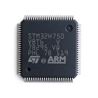
STM32H750VBT6TR - 480MHz Cortex-M7 MCU, 128KB Flash | STMicroelectronics (Tape & Reel)
MPN: STM32H750VBT6TR ✓ פעילSTM32H750VBT6TR סקירה
A microcontroller (MCU) is a compact integrated circuit that combines a processor core, memory, and programmable I/O peripherals on a single die to govern a specific embedded operation. The STM32H750VBT6TR sits at the top of the STM32H7 Value-Line hierarchy, which itself belongs to the broader STMicroelectronics STM32 family of 32-bit Arm Cortex-M microcontrollers, placing it well above mainstream families such as the STM32F4 in both clock speed and peripheral richness.
Key features include the 480 MHz Cortex-M7 core with DP-FPU and L1 cache, 1 MB of SRAM paired with only 128 KB of internal flash (a deliberate value-line trade-off that encourages executing code from external memory or XSPI RAM), a hardware cryptographic accelerator for AES/DES/3DES/HASH/SHA, and a rich connectivity set with 46 communication interfaces including USART, SPI, I2C, FDCAN, USB OTG, Ethernet MAC, an SDMMC, a TFT-LCD controller, a DCMI camera interface, and the Chrom-ART graphics accelerator. The device operates from a 1.62 V to 3.6 V supply across -40 C to +85 C.
Architecturally, the device integrates an MPU, an NVIC with hardware tail chaining, and four flexible power modes (Run, Sleep, Stop, Standby) managed through an internal SMPS-capable voltage regulator that can be configured to balance performance versus consumption. The Cortex-M7 superscalar pipeline with branch prediction delivers 2.14 DMIPS/MHz and a CoreMark score in the hundreds per MHz.
Typical applications include industrial motor drives and power conversion, medical instrumentation, smart-home and audio hubs, and HMI/graphics systems where 480 MHz throughput, 1 MB on-chip RAM, and LCD/camera interfaces remove the need for external memory in many designs.
Design consideration: with only 128 KB of internal flash, large applications must run from XSPI external memory or internal RAM, so budget code placement and boot configuration early in the project lifecycle.
This page synthesizes distributor pricing, drop-in alternatives, and practical design notes not found in the manufacturer datasheet alone.
חלופות תחליף ישיר עבור STM32H750VBT6TR — אותו מארז, תואם פין-לפין. חלקים במארז שונה הדורשים עיבוד מחדש של ה-PCB אינם נכללים.
STM32H753VIT6
📋 חלופה להתייחסות (לא בקטלוג)
STM32F746VGT6
צור קשר לקבלת מחיר
הצג גיליון נתונים ←STM32H750VBT6TR דירוגים מרביים ומאפיינים חשמליים
| Core Architecture | Arm Cortex-M7 with double-precision FPU |
| תדר שעון מקסימלי | 480 MHz |
| Program Flash Memory | 128 KB |
| SRAM | 1 MB (256 KB DTCM + 256 KB AXI SRAM + 64 KB ITCM + 4 KB backup SRAM) |
| Supply Voltage (VDD) | 1.62 V to 3.6 V |
| טמפרטורת פעולה | -40 C to +85 C (grade 6) |
| מארז | LQFP-100 (14x14 mm, 0.5 mm pitch) |
| Communication Interfaces | 46 (USART/UART, SPI, I2C, FDCAN, USB OTG FS+HS, Ethernet MAC, SDMMC, SAI) |
| Display Controller | TFT-LCD controller (LTDC) |
| Camera Interface | DCMI 8/14-bit parallel |
| Cryptographic Accelerator | AES/DES/3DES/HASH/SHA, true RNG |
| Graphics Accelerator | Chrom-ART (DMA2D) |
| סוג הרכבה | Surface Mount |
| רמת MSL | 3 |
| סטטוס RoHS | Compliant (ROHS3) |
תצורת פינים של STM32H750VBT6TR
| פין 1 | PE2 — GPIO PE2 / TRACECLK / SPI4_SCK / SAI1_MCLK_A / TIM9_CH1 / ETH_MII_TXD3 / DCMI_D3 |
| פין 2 | PE3 — GPIO PE3 / TRACED0 / SAI1_SD_B / TIM15_CH2 / USART1_RX |
| פין 3 | PE4 — GPIO PE4 / TRACED1 / SPI4_NSS / SAI1_FS_A / TIM15_CH1N / DCMI_D4 |
| פין 4 | PE5 — GPIO PE5 / TRACED2 / TIM9_CH1 / SPI4_MISO / SAI1_SCK_A / DCMI_D5 |
| פין 5 | PE6 — GPIO PE6 / TRACED3 / TIM1_BKIN2 / SPI4_MOSI / SAI1_SD_A / TIM15_CH2 / DCMI_D6 |
| פין 6 | VBAT — Backup battery supply input |
| פין 7 | PC13 — GPIO PC13 / RTC_TS1 / WKUP3 (tamper pin) |
| פין 8 | PC14 — GPIO PC14 / OSC32_IN (LSE crystal) |
| פין 9 | PC15 — GPIO PC15 / OSC32_OUT (LSE crystal) |
| פין 10 | VSS — Ground |
| פין 11 | VDD — Digital supply 1.62-3.6 V |
| פין 12 | PH0 — GPIO PH0 / OSC_IN (HSE crystal) |
| פין 13 | PH1 — GPIO PH1 / OSC_OUT (HSE crystal) |
| פין 14 | NRST — Active-low reset input |
| פין 15 | PC0 — GPIO PC0 / ADC1_INP10 / SAI1_FS_B / OTG_HS_ULPI_STP / DFSDM1_CKIN0 |
| פין 16 | PC1 — GPIO PC1 / ADC1_INP11 / SAI1_MCLK_B / SDMMC2_CD / ETH_MDC / DFSDM1_DATIN1 |
| פין 17 | PC2 — GPIO PC2 / ADC1_INP12 / SPI2_MISO / OTG_HS_ULPI_DIR / ETH_MII_TXD2 / DFSDM1_CKIN1 |
| פין 18 | PC3 — GPIO PC3 / ADC1_INP13 / SPI2_MOSI / OTG_HS_ULPI_NXT / ETH_MII_TX_CLK / DFSDM1_DATIN2 |
| פין 19 | VSSA — Analog ground |
| פין 20 | VDDA — Analog supply 1.62-3.6 V |
| פין 21 | PA0 — GPIO PA0 / ADC1_INP0 / TIM2_CH1 / TIM5_CH1 / USART2_CTS / UART4_TX / SAI1_SD_B / ETH_MII_CRS |
| פין 22 | PA1 — GPIO PA1 / ADC1_INP1 / TIM2_CH2 / TIM5_CH2 / USART2_RTS / UART4_RX / SAI1_MCLK_B / ETH_MII_RX_CLK |
| פין 23 | PA2 — GPIO PA2 / ADC1_INP2 / TIM2_CH3 / TIM5_CH3 / USART2_TX / SAI1_SCK_B / ETH_MDIO |
| פין 24 | PA3 — GPIO PA3 / ADC1_INP3 / TIM2_CH4 / TIM5_CH4 / USART2_RX / OTG_HS_ULPI_D0 / ETH_MII_COL |
| פין 25 | VSS — Ground |
| פין 26 | VDD — Digital supply 1.62-3.6 V |
| פין 27 | PA4 — GPIO PA4 / ADC1_INP4 / DAC1_OUT1 / SPI1_NSS / SPI3_NSS / USART2_CK / OTG_HS_SOF / DCMI_HSYNC |
| פין 28 | PA5 — GPIO PA5 / ADC1_INP5 / DAC1_OUT2 / TIM2_CH1 / TIM8_CH1N / SPI1_SCK / OTG_HS_ULPI_CK |
| פין 29 | PA6 — GPIO PA6 / ADC1_INP6 / TIM2_CH1 / TIM8_CH1 / SPI1_MISO / TIM13_CH1 / DCMI_PIXCLK |
| פין 30 | PA7 — GPIO PA7 / ADC1_INP7 / TIM2_CH2 / TIM8_CH2 / SPI1_MOSI / TIM14_CH1 / ETH_MII_RX_DV / RMII_CRS_DV |
| פין 31 | PC4 — GPIO PC4 / ADC2_INP4 / I2S1_MCK / SPDIFRX_IN0 / OTG_HS_ULPI_STP / ETH_MII_RXD0 / RMII_RXD0 |
| פין 32 | PC5 — GPIO PC5 / ADC2_INP5 / SAI1_SD_A / SPDIFRX_IN1 / OTG_HS_ULPI_CK / ETH_MII_RXD1 / RMII_RXD1 |
| פין 33 | PB0 — GPIO PB0 / ADC1_INP8 / TIM1_CH2N / TIM8_CH2N / OTG_HS_ULPI_D1 / ETH_MII_RXD2 / DFSDM1_CKOUT |
| פין 34 | PB1 — GPIO PB1 / ADC1_INP9 / TIM1_CH3N / TIM8_CH3N / OTG_HS_ULPI_D2 / ETH_MII_RXD3 / DFSDM1_DATIN3 |
| פין 35 | PB2 — GPIO PB2 / I2S1_SD / SPI3_MOSI / SAI1_SD_A / TIM15_CH1N / OTG_HS_ULPI_D4 / ETH_MII_TXD1 |
| פין 36 | PF0 — GPIO PF0 / I2C2_SDA / I2S1_WS / OTG_HS_ULPI_D5 / TIM23_CH1 / DFSDM1_CKIN0 |
| פין 37 | PF1 — GPIO PF1 / I2C2_SCL / I2S1_CK / OTG_HS_ULPI_D6 / TIM23_CH2 / DFSDM1_CKIN1 |
| פין 38 | PF2 — GPIO PF2 / I2C2_SMBA / SAI1_SD_B / USART3_RTS / OTG_HS_ULPI_D7 / TIM23_CH3 / DFSDM1_CKIN2 |
| פין 39 | PF3 — GPIO PF3 / ADC3_INP5 / SAI1_MCLK_B / USART3_CTS / OTG_HS_ULPI_NXT / TIM23_CH4 / DFSDM1_CKIN3 |
| פין 40 | PF4 — GPIO PF4 / ADC3_INP6 / SAI1_SCK_B / TRACED0 / USART3_TX / DFSDM1_CKOUT |
| פין 41 | PF5 — GPIO PF5 / ADC3_INP7 / SAI1_FS_B / TRACED1 / USART3_RX / DFSDM1_DATIN0 |
| פין 42 | VSS — Ground |
| פין 43 | VDD — Digital supply 1.62-3.6 V |
| פין 44 | PF6 — GPIO PF6 / ADC3_INP8 / SAI1_SD_A / TIM16_CH1 / SPI5_NSS / SAI1_DFSDM1_DATIN1 |
| פין 45 | PF7 — GPIO PF7 / ADC3_INP9 / SAI1_MCLK_A / TIM17_CH1 / SPI5_SCK / DFSDM1_DATIN2 |
| פין 46 | PF8 — GPIO PF8 / ADC3_INP10 / SAI1_SCK_A / TIM13_CH1 / SPI5_MISO / DFSDM1_CKIN3 |
| פין 47 | PF9 — GPIO PF9 / ADC3_INP11 / SAI1_FS_A / TIM14_CH1 / SPI5_MOSI / DFSDM1_DATIN3 |
| פין 48 | PF10 — GPIO PF10 / ADC3_INP12 / SAI1_SD_B / TIM16_CH1N / SAI1_DFSDM1_CKOUT |
| פין 49 | PH2 — GPIO PH2 / I2C2_SCL / SPI5_SD / OTG_HS_ULPI_STP / ETH_MII_CRS |
| פין 50 | PH3 — GPIO PH3 / I2C2_SDA / SPI5_CK / OTG_HS_ULPI_DIR / ETH_MII_COL |
| פין 51 | PH4 — GPIO PH4 / I2C1_SCL / SPI5_WS / OTG_HS_ULPI_NXT |
| פין 52 | PH5 — GPIO PH5 / I2C1_SDA / SPI5_NSS / OTG_HS_ULPI_CK |
| פין 53 | VSS — Ground |
| פין 54 | VDD — Digital supply 1.62-3.6 V |
| פין 55 | PA8 — GPIO PA8 / TIM1_CH1 / TIM8_CH1 / USART1_CK / OTG_FS_SOF / TIM14_CH1 / SAI1_SD_A_M6 |
| פין 56 | PA9 — GPIO PA9 / TIM1_CH2 / USART1_TX / SPI2_SCK / SAI1_FS_A / OTG_FS_VBUS |
| פין 57 | PA10 — GPIO PA10 / TIM1_CH3 / USART1_RX / SPI2_MISO / OTG_FS_ID / SAI1_SD_A_M5 |
| פין 58 | PA11 — GPIO PA11 / TIM1_CH4 / USART1_CTS / CAN1_RX / OTG_FS_DM |
| פין 59 | PA12 — GPIO PA12 / TIM1_ETR / USART1_RTS / CAN1_TX / OTG_FS_DP / SAI1_SCK_A |
| פין 60 | PA13 — GPIO PA13 / JTMS / SWDIO |
| פין 61 | VDD — Digital supply 1.62-3.6 V |
| פין 62 | VSS — Ground |
| פין 63 | PA14 — GPIO PA14 / JTCK / SWCLK |
| פין 64 | PA15 — GPIO PA15 / JTDI / SPI1_NSS / SPI3_NSS / SPI6_NSS / UART4_RTS / TIM2_CH1 / TIM8_CH1 |
| פין 65 | PC6 — GPIO PC6 / TIM3_CH1 / TIM8_CH1 / I2S2_MCK / USART6_TX / SDMMC1_D0 / DCMI_D0 / TIM12_CH1 |
| פין 66 | PC7 — GPIO PC7 / TIM3_CH2 / TIM8_CH2 / I2S2_CK / SPI2_SCK / USART6_RX / SDMMC1_D1 / DCMI_D1 / TIM12_CH2 |
| פין 67 | PC8 — GPIO PC8 / TIM3_CH3 / TIM8_CH3 / I2S2_SD / SPI2_MISO / USART6_CK / SDMMC1_D2 / DCMI_D2 / TIM13_CH1 |
| פין 68 | PC9 — GPIO PC9 / TIM3_CH4 / TIM8_CH4 / I2S2_WS / SPI2_MOSI / MCO2 / SDMMC1_D3 / DCMI_D3 / TIM14_CH1 |
| פין 69 | PA15 — GPIO PA15 (alt) |
| פין 70 | VDD — Digital supply 1.62-3.6 V |
| פין 71 | VSS — Ground |
| פין 72 | PB3 — GPIO PB3 / JTDO / TRACESWO / SPI1_SCK / SPI3_SCK / USART1_RX / TIM2_CH2 / SAI1_SCK_B |
| פין 73 | PB4 — GPIO PB4 / NJTRST / SPI1_MISO / SPI3_MISO / USART1_TX / TIM3_CH1 / SAI1_FS_B / OTG_HS_ULPI_D0 |
| פין 74 | PB5 — GPIO PB5 / SPI1_MOSI / SPI3_MOSI / USART1_CK / TIM3_CH2 / I2C1_SMBA / SAI1_SD_B / OTG_HS_ULPI_D1 |
| פין 75 | PB6 — GPIO PB6 / TIM2_CH3 / I2C1_SCL / USART1_TX / CAN2_TX / SPI4_SCK / OTG_FS_SOF |
| פין 76 | PB7 — GPIO PB7 / TIM2_CH4 / I2C1_SDA / USART1_RX / CAN2_RX / SPI4_NSS / I2S1_CK / SAI1_SD_A |
| פין 77 | BOOT0 — Boot mode selection (0 = main flash, 1 = bootloader/system memory) |
| פין 78 | PB8 — GPIO PB8 / TIM4_CH3 / I2C1_SCL / CAN1_RX / SDMMC1_D4 / OTG_FS_SOF / SAI1_DFSDM1_CKOUT |
| פין 79 | PB9 — GPIO PB9 / TIM4_CH4 / I2C1_SDA / SPI2_NSS / CAN1_TX / SDMMC1_D5 / I2S2_WS / SDMMC1_CD |
| פין 80 | PE0 — GPIO PE0 / TIM4_ETR / UART8_RX / SPI3_MISO / SPI5_MISO / TIM23_ETR / DCMI_D0 |
| פין 81 | PE1 — GPIO PE1 / TIM4_CH2 / UART8_TX / SPI3_MOSI / SPI5_MOSI / DCMI_D1 |
| פין 82 | VSS — Ground |
| פין 83 | VDD — Digital supply 1.62-3.6 V |
| פין 84 | PB10 — GPIO PB10 / TIM2_CH3 / I2C2_SCL / SPI2_SCK / USART3_TX / OTG_FS_ID / SAI1_SCK_A |
| פין 85 | PB11 — GPIO PB11 / TIM2_CH4 / I2C2_SDA / SPI2_MISO / USART3_RX / OTG_FS_DM / SAI1_SD_A |
| פין 86 | PB12 — GPIO PB12 / TIM1_BKIN / I2C2_SMBA / SPI2_NSS / USART3_CK / CAN2_RX / OTG_HS_ID / SAI1_FS_A |
| פין 87 | PB13 — GPIO PB13 / TIM1_CH1N / SPI2_SCK / USART3_CTS / CAN2_TX / OTG_HS_VBUS / SAI1_SCK_A |
| פין 88 | PB14 — GPIO PB14 / TIM1_CH2N / SPI2_MISO / USART3_RTS / TIM12_CH1 / OTG_HS_DM / SAI1_SD_A |
| פין 89 | PB15 — GPIO PB15 / TIM1_CH3N / SPI2_MOSI / TIM12_CH2 / OTG_HS_DP / SAI1_FS_A |
| פין 90 | PD0 — GPIO PD0 / TIM4_CH3 / I2C3_SDA / SAI3_SD_A / UART4_RX / SDMMC1_CMD / DFSDM1_DATIN7 |
| פין 91 | PD1 — GPIO PD1 / TIM4_CH4 / I2C3_SCL / SAI3_SD_B / UART4_TX / SDMMC1_CKIN / DFSDM1_CKIN7 |
| פין 92 | VSS — Ground |
| פין 93 | VDD — Digital supply 1.62-3.6 V |
| פין 94 | PD2 — GPIO PD2 / TIM3_ETR / UART5_RX / SDMMC1_CMD / DCMI_D11 / SAI3_SD_A |
| פין 95 | PD3 — GPIO PD3 / TIM2_CH1 / USART2_CTS / SDMMC1_D0 / DCMI_D5 / SAI3_SD_B |
| פין 96 | PD4 — GPIO PD4 / TIM2_CH2 / USART2_RTS / SDMMC1_D1 / DCMI_D6 / SAI3_FS_A |
| פין 97 | PD5 — GPIO PD5 / TIM2_CH3 / USART2_TX / SDMMC1_D2 / DCMI_D7 / SAI3_SCK_A |
| פין 98 | PD6 — GPIO PD6 / TIM2_CH4 / SAI1_SD_A / USART2_RX / SDMMC1_D3 / DCMI_D8 / SAI3_MCLK_A |
| פין 99 | PD7 — GPIO PD7 / TIM2_CH1 / USART2_CK / SDMMC1_D4 / DCMI_D9 / SAI1_SD_B |
| פין 100 | PG15 — GPIO PG15 / USART6_CTS / UART7_CTS / DCMI_D13 |
יישומים טיפוסיים
STM32H750VBT6TR מתאים עבור 7 יישוםs: Industrial Motor Drives and Field-Oriented Control, HMI and Graphics Display Terminals, Medical Instrumentation and Patient Monitoring, Audio Hub and Smart Home Speakers, Vision and Camera-Based Inspection, Industrial IoT Edge Gateways, Power Conversion and Digital SMPS Control.
Industrial Motor Drives and Field-Oriented Control
The STM32H750VBT6TR is well matched to industrial FOC motor drives. The 480 MHz Cortex-M7 with DP-FPU executes Park/Clarke transforms and SVM in well under 1 microsecond per PWM period, while the integrated HRTIM timer generates center-aligned PWM at the resolutions required for 50 kHz+ switching frequencies. Per the STM32H750VB datasheet, the 1 MB of SRAM (DTCM + AXI + ITCM) holds the entire FOC state machine plus a sensorless observer, removing the need for external memory. Three 12-bit ADCs sampled at 2.7 MSPS deliver simultaneous shunt current sensing, and FDCAN enables integration with industrial fieldbus networks. The -40 C to +85 C industrial temperature grade supports factory-floor deployment without derating.
מומלץ
HMI and Graphics Display Terminals
The STM32H750VBT6TR drives HMI panels without external graphics memory. The integrated TFT-LCD LTDC controller supports up to XGA resolution, the Chrom-ART (DMA2D) accelerator offloads rectangular fills and pixel-format conversions, and the 1 MB of AXI SRAM holds framebuffers for typical 4.3-inch to 7-inch WVGA displays. Per the STM32H750VB datasheet, the 480 MHz Cortex-M7 runs LVGL/Embedded Wizard graphics stacks comfortably with 60 Hz refresh, while SDMMC and OSPI interfaces allow asset storage from microSD or external flash. The LQFP-100 footprint suits compact panel-mount designs where cost is sensitive.
מומלץ
Medical Instrumentation and Patient Monitoring
The STM32H750VBT6TR suits portable patient monitoring and diagnostic instruments. The 480 MHz core processes DSP-intensive ECG/PPG/SpO2 algorithms in real time, the 1 MB SRAM holds large waveform buffers, and the AES/SHA hardware crypto secures wireless patient-data links. Per the STM32H750VB datasheet, the low-power Stop/Standby modes drop consumption to microampere levels for battery operation between measurements. USB OTG FS+HS simplifies tethered diagnostic interfaces, while the 1.62-3.6 V supply range supports single-cell Li-ion designs with no extra LDO. LQFP-100 footprint eases hand-soldered prototype builds.
מומלץ
Audio Hub and Smart Home Speakers
The STM32H750VBT6TR functions as the main processor in audio hubs. The SAI interface drives external DACs for multi-room audio, while the Cortex-M7 at 480 MHz runs DSP effects, voice wake-word recognition, and HTTP/MQTT stacks simultaneously. Per the STM32H750VB datasheet, the 1 MB SRAM holds large audio buffers and streaming metadata without external memory, and Ethernet MAC plus USB OTG HS enable both wired and wireless dongle connectivity. The low standby current suits always-listening voice hubs, while the LQFP-100 package supports consumer-grade cost targets.
מומלץ
Vision and Camera-Based Inspection
The STM32H750VBT6TR captures and processes image data from the integrated DCMI parallel port. The 480 MHz core executes JPEG compression and simple blob/edge-detection algorithms, while Chrom-ART accelerates pixel pipeline operations. Per the STM32H750VB datasheet, the 1 MB SRAM holds multiple QVGA/VGA framebuffers for short inspection cycles, and SDMMC writes captured images to microSD. The hardware SHA/AES block secures inspection logs. Operating from -40 C to +85 C supports industrial camera installations without thermal enclosure.
מומלץ
Industrial IoT Edge Gateways
The STM32H750VBT6TR acts as an edge gateway in industrial IoT deployments. The Cortex-M7 at 480 MHz handles Modbus/Profinet/EtherCAT bridging, while Ethernet MAC plus FDCAN interface to industrial fieldbus. Per the STM32H750VB datasheet, the 1 MB SRAM buffers high-rate sensor streams and TLS-secured MQTT publishes without external memory, and the hardware AES/SHA accelerators secure wireless uplinks. The low-power Run mode keeps standby consumption manageable for solar/battery deployments, and the -40 C to +85 C temperature range suits outdoor enclosures.
מומלץ
Power Conversion and Digital SMPS Control
The STM32H750VBT6TR implements digital control loops in high-performance SMPS converters. The HRTIM timer generates multi-phase PWM with sub-100 ns resolution, while the Cortex-M7 executes digital current-mode control and adaptive dead-time algorithms within a single switching cycle. Per the STM32H750VB datasheet, three high-speed 12-bit ADCs sampled at 2.7 MSPS enable valley-current sensing and input voltage feedforward, and the 1 MB SRAM holds lookup tables for non-linear magnetics compensation. Operating from -40 C to +85 C supports telecom and industrial power stages.
מומלץ
סיכום מוצרים מומלצים
נתוני עזר הנדסיים עבור STM32H750VBT6TR — השוואה, הנחיות תכנון ומידע על תאימות.
מדריך בחירה
השוואה עם חלופות
| פרמטר | מוצר זה | STM32H750VBT6TRTR | STM32H743VIT6 | STM32H753VIT6 | STM32F746VGT6 | STM32H742VIT6 |
|---|---|---|---|---|---|---|
| Brand | STMicroelectronics | STMicroelectronics | STMicroelectronics | STMicroelectronics | STMicroelectronics | STMicroelectronics |
| Package | LQFP-100 (14x14 mm) | LQFP-100 (14x14 mm) - same | LQFP-100 (14x14 mm) - same | LQFP-100 (14x14 mm) - same | LQFP-100 (14x14 mm) - same | LQFP-100 (14x14 mm) - same |
| Core | Cortex-M7 480 MHz | Cortex-M7 480 MHz | Cortex-M7 480 MHz | Cortex-M7 480 MHz | Cortex-M7 216 MHz | Cortex-M7 480 MHz |
| Flash Memory | 128 KB | 128 KB | 2 MB | 2 MB | 1 MB | 2 MB |
| SRAM | 1 MB | 1 MB | 1 MB | 1 MB | 320 KB | 1 MB |
| Crypto Accelerator | AES/DES/3DES/SHA + RNG | AES/DES/3DES/SHA + RNG | AES/DES/SHA + RNG | AES/DES/SHA + RNG (crypto-grade) | AES/DES/SHA + RNG | AES/DES/SHA + RNG |
| Supply Voltage | 1.62-3.6 V | 1.62-3.6 V | 1.62-3.6 V | 1.62-3.6 V | 1.7-3.6 V | 1.62-3.6 V |
| Operating Temperature | -40 C to +85 C | -40 C to +85 C | -40 C to +85 C | -40 C to +85 C | -40 C to +85 C | -40 C to +85 C |
| Indicative Price (qty 100) | USD 11.85 | USD 11.85 | USD 14.50 | USD 16.20 | USD 8.10 | USD 14.50 |
מבדילים עיקריים
- Value-Line H7 with 1 MB SRAM and only 128 KB flash (לעומתSTM32H743VIT6)
- Cost-optimized Cortex-M7 480 MHz in LQFP-100 (לעומתSTM32F746VGT6)
- Same LQFP-100 footprint as mainstream H7 family (לעומתSTM32H750IBT6 (LQFP-176))
הערות תכנון
The STM32H750VBT6TR supports both LDO and SMPS power modes via PWR_LDO_SOC and PWR_SOC_SEL bits in PWR control register 1. For high-throughput DSP workloads at 480 MHz, configure the SMPS regulator for high-power mode (PWR_SOC_SEL = 1) to deliver the full 1 A core current; for battery-powered Stop/Standby entry, the SMPS drops to low-power mode and quiescent current falls below the datasheet Stop1 value. Always place 100 nF + 4.7 uF ceramic decoupling close to each VDD pin pair per ST AN5419 reference design.
At 480 MHz core clock with all peripherals enabled, the STM32H750VBT6TR consumes roughly 200 mA from VDD core. With theta_JA of approximately 40 C/W for LQFP-100 on a 4-layer JEDEC test PCB, the die rises about 8 C above ambient - comfortably within the -40 C to +85 C industrial range. Estimated: P_core = 0.2 A * 1.0 V = 0.2 W, T_rise = 0.2 W * 40 C/W = 8 C. Add a 10x10 mm copper pour under the exposed pad area for headroom if peripherals are pushed to full bus bandwidth simultaneously.
Layout the XSPI/OSPI interface to external flash with length-matched 50 ohm traces within 25 mm of the LQFP-100 pins to maintain signal integrity at 200 MHz DDR modes per the H7 hardware design recommendations. Route SDMMC1 to a microSD holder with ground-via stitching between data lines, and place the HSE 8 MHz crystal + load caps within 5 mm of PH0/PH1 to avoid start-up failures. Place boot mode 0.x mode pins through 10 kohm pull resistors to keep bootloader selection stable at power-up.
Do not rely on internal flash for large applications - the 128 KB flash on STM32H750VBT6TR is sized to hold a bootloader only; user firmware should be linked to execute from XSPI external memory (XIP mode) or copied into AXI SRAM at startup. Configure the boot pins (BOOT0/BOOT1) to select XSPI boot for production, and verify that your flash loader works with the bundled STM32CubeProgrammer. Watch out: using JTAG/SWD while the FDCAN or USB OTG HS lines are active can trigger errata USB reset on first-time programming.
The Ethernet MAC on STM32H750VBT6TR requires an external PHY (e.g., LAN8742) and proper 50 ohm impedance on MII/RMII traces. Per the H7 datasheet, RMII is the recommended interface for LQFP-100 designs because it minimizes pin count; route RMII_REF_CLK with controlled impedance within 25 mm of the PHY. The DCMI camera interface benefits from series damping resistors (33 ohm) on each data line when the bus exceeds 50 MHz pixel clock.
מידע על תאימות
Per ST product page: ROHS3 compliant, REACH compliant, MSL 3 packaging. Industrial-grade -40 C to +85 C only - no AEC-Q100 automotive variant in this MPN suffix.