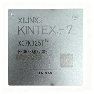
XC5VLX110-2FF676I - 110K Cell Virtex-5 LX FPGA | AMD
MPN: XC5VLX110-2FF676I ✓ פעילXC5VLX110-2FF676I סקירה
A field-programmable gate array is a semiconductor device whose digital logic functions are configured after manufacture. In the product hierarchy, an FPGA is a programmable logic device and therefore a specialized semiconductor integrated circuit. Virtex-5 LX devices target designs requiring substantial parallel processing, flexible interfaces, and high-speed programmable logic without the expense of designing a custom ASIC.
The principal device characteristics are 110,592 logic cells, 440 I/O, and a 676-BBGA FCBGA package. The listed 4,718,592 device parameter is consistent with the block-memory capacity class of the Virtex-5 LX family, while the -2 ordering suffix identifies the selected speed grade. The 676-contact FCBGA package supports dense board-level integration but requires careful escape routing, thermal design, and BGA assembly control.
Technically, the XC5VLX110 belongs to the 65 nm CMOS Virtex-5 LX generation and provides a large programmable fabric for parallel data processing, interface bridging, protocol conversion, and embedded control. The 440-user I/O complement is important for systems with numerous external buses, yet actual usable I/O can be lower when dedicated configuration, clock, power, and other package assignments are considered. Signal-integrity, banking, and pin-placement constraints must be checked in the device constraints before layout.
Typical applications include high-throughput data acquisition, communications infrastructure, industrial imaging, test and measurement, embedded signal processing, and network equipment. The large logic-cell count supports parallel datapaths and multi-clock subsystems, while the broad I/O count simplifies connections to external memory, transceivers, converters, and high-speed interfaces.
The primary design challenge is the dense FCBGA footprint. Use the AMD package pinout files when assigning power, ground, configuration pins, and I/O standards, and validate every high-speed interface against the published package and device constraints. Power rails, decoupling, thermal vias, and external memory topology require careful sign-off because package escape-routing space is limited.
This product page combines the device identity, package details, drop-in ordering-code alternatives, application guidance, and engineering design notes in one place. It also distinguishes true same-footprint options from alternatives requiring different speed grades, temperature grades, or logic density.
חלופות תחליף ישיר עבור XC5VLX110-2FF676I — אותו מארז, תואם פין-לפין. חלקים במארז שונה הדורשים עיבוד מחדש של ה-PCB אינם נכללים.
וריאנטים בסדרה זו
דגמים מאותה סדרה התואמים Drop-in עם XC5VLX110-2FF676I (אותו גורם צורה וטביעת רגל) — שונים ב Device Type, Package Type, Temperature Grade, Logic Cells, Speed Grade.
XC5VLX110-2FFG676I
✅ Drop-In📋 חלופה להתייחסות (לא בקטלוג)
XC5VLX110-1FF676I
✅ Drop-Inצור קשר לקבלת מחיר
הצג גיליון נתונים ←XC5VLX110-1FF676C
✅ Drop-Inצור קשר לקבלת מחיר
הצג גיליון נתונים ←XC5VLX110-2FF676C
✅ Drop-In ⚠️ מפרטים לא מאומתיםצור קשר לקבלת מחיר
הצג גיליון נתונים ←XC5VLX85-2FF676I
✅ Drop-Inצור קשר לקבלת מחיר
הצג גיליון נתונים ←XC5VLX110-2FF676I דירוגים מרביים ומאפיינים חשמליים
| Device Type | Virtex-5 LX Field Programmable Gate Array |
| Logic Cells | 110,592 cells |
| User I/O | 440 I/O |
| Device Memory Parameter | 4,718,592 bits |
| Process Technology | 65 nm CMOS |
| Core Supply Voltage | 1 V |
| Performance Grade | -2 |
| Temperature Grade | Industrial |
| Package Type | 676-BBGA, FCBGA |
| מספר פינים | 676 pins |
| סוג הרכבה | Surface Mount |
| FPGA Family | Virtex-5 LX |
| Programmable Logic | FPGA |
מדריך תצורת פינים של XC5VLX110-2FF676I 676-bbga, fcbga
תצורת פינים עבור XC5VLX110-2FF676I (מארזת 676-bbga, fcbga). מעגל משולב דיגיטלי זה כולל GPIO, ממשקי תקשורת (UART, SPI, I2C) ופיני מתח. יש לעיין בגיליון הנתונים של היצרן לפונקציות פינים חלופיות ולאפשרויות תצורה. חיוני לתכנון מערכות משובצות ולפריסת PCB.

אין נתוני פריסת פינים מפורטים עבור XC5VLX110-2FF676I.
עיינו ב- גיליון נתונים עבור תצורת פינים מלאה.
יישומים טיפוסיים
XC5VLX110-2FF676I מתאים עבור 6 יישוםs: High-Speed Data Acquisition, Communications Infrastructure, Industrial Imaging and Signal Processing, Test and Measurement Equipment, Network Storage and Interface Bridging, Aerospace and Defense Control Systems.
High-Speed Data Acquisition
The XC5VLX110-2FF676I fits parallel data-acquisition systems that must capture, filter, and route many channels while maintaining deterministic FPGA timing. Its 110,592 logic cells provide substantially more parallel processing capacity than the XC5VLX85-2FF676I, while 440 user I/O simplify connections to multiple converters, clocks, and data-control signals. Designers can implement acquisition pipelines, digital filtering, packetization, and interface conversion in one configurable device. The -2 performance grade should be checked against the system timing budget, while the 676-pin FCBGA demands a BGA-qualified PCB stack-up, dense power delivery, and package-aware escape routing.
מומלץ
Communications Infrastructure
The XC5VLX110-2FF676I is suitable for communications infrastructure requiring parallel packet processing, clock-domain management, and flexible high-speed interfaces. Its large 110,592-cell programmable fabric can host protocol engines, queues, scrambling functions, and test logic, while the 440 I/O count supports substantial board-level connectivity. The device is especially relevant to legacy or long-lifecycle designs standardized on Virtex-5 LX. Engineers should preserve the exact device constraints when migrating to the XC5VLX110-2FFG676I and should use the -1 grade alternatives only after post-route timing analysis. Power, clock jitter, and signal-integrity margins are especially important in line-card and network-equipment deployments.
מומלץ
Industrial Imaging and Signal Processing
The XC5VLX110-2FF676I can support industrial imaging and real-time signal-processing systems that combine parallel sensor interfaces with substantial on-device computation. The 110,592 logic cells allow designers to implement pixel pipelines, feature extraction, motion processing, and control functions in programmable logic, while 440 I/O provide connections to image sensors, memory, and external converters. The industrial-temperature ordering option makes the part appropriate for temperature-qualified equipment designs, subject to confirmation of the exact operating range. A 676-pin FCBGA requires careful escape routing and thermal-via placement, and clocking should be planned around the package’s assigned clock-capable pins and supported I/O standards.
מומלץ
Test and Measurement Equipment
The XC5VLX110-2FF676I is useful in test and measurement instruments that require configurable timing, dense acquisition logic, and multiple instrument-control interfaces. Its 110,592-cell fabric can implement pattern generation, protocol analysis, trigger logic, digital correction, and real-time processing, while the 440 I/O provide broad instrument connectivity. The -2 grade supports designs with demanding timing margins, although actual timing closure depends on the selected clocking, I/O standards, routing, and device utilization. For long-lived laboratory equipment, preserve the exact device, speed, and temperature ordering codes during maintenance. Board construction should follow the package-specific BGA rules and include adequate thermal spreading under this large FCBGA package.
מומלץ
Network Storage and Interface Bridging
The XC5VLX110-2FF676I can bridge multiple external interfaces in network storage, server-adjacent, and data-center equipment where a fixed ASIC would be inflexible. The 110,592 logic cells support high-throughput datapaths, buffering, protocol conversion, error checking, and control logic, while 440 I/O facilitate connections to memory and transceiver components. The 676-pin FCBGA offers dense integration but limits escape-routing space, so designers should allocate package balls and layer transitions early using the device-specific constraints. When selecting the XC5VLX85-2FF676I, verify that the approximately 25-percent smaller cell count is sufficient. Power estimation must reflect the actual configuration because FPGA consumption varies substantially with utilized logic and I/O activity.
מומלץ
Aerospace and Defense Control Systems
The XC5VLX110-2FF676I can support long-lifecycle embedded-control and mission-processing prototypes that need reconfigurable logic, broad I/O, and a large Virtex-5 LX fabric. Programmable resources can implement control loops, protocol stacks, fault handling, and test logic, while 440 I/O allow extensive connections to sensors, memory, and communication equipment. The industrial-temperature ordering option should be checked against the system’s exact environmental envelope and qualification requirements. Timing must be demonstrated with the -2 grade rather than assumed from an XC5VLX110-1FF676I alternative. For deployed systems, review the current product lifecycle, reliability documentation, configuration-security controls, and BGA manufacturing capability with the manufacturer.
מומלץ
סיכום מוצרים מומלצים
נתוני עזר הנדסיים עבור XC5VLX110-2FF676I — השוואה, הנחיות תכנון ומידע על תאימות.
מדריך בחירה
השוואה עם חלופות
| פרמטר | מוצר זה | XC5VLX110-2FFG676I | XC5VLX110-1FF676I | XC5VLX110-1FF676C | XC5VLX110-2FF676C | XC5VLX85-2FF676I |
|---|---|---|---|---|---|---|
| Brand | AMD | AMD | AMD | AMD | AMD | AMD |
| Package | 676-BBGA, FCBGA | 676-BBGA, FCBGA | 676-BBGA, FCBGA | 676-BBGA, FCBGA | 676-BBGA, FCBGA | 676-BBGA, FCBGA |
| FPGA Family | Virtex-5 LX | Virtex-5 LX | Virtex-5 LX | Virtex-5 LX | Virtex-5 LX | Virtex-5 LX |
| Logic Cells | 110,592 cells | 110,592 cells | 110,592 cells | 110,592 cells | 110,592 cells | 82,944 cells |
| User I/O | 440 I/O | 440 I/O | 440 I/O | 440 I/O | 440 I/O | 440 I/O |
| Process Technology | 65 nm CMOS | 65 nm CMOS | 65 nm CMOS | 65 nm CMOS | 65 nm CMOS | 65 nm CMOS |
| Core Supply Voltage | 1 V | 1 V | 1 V | 1 V | 1 V | 1 V |
| Speed Grade | -2 | -2 | -1 | -1 | -2 | -2 |
| Temperature Suffix | I (industrial) | I (industrial) | I (industrial) | C (commercial) | C (commercial) | I (industrial) |
| Special Features | Virtex-5 LX with -2 speed grade and industrial-temperature ordering code | Virtex-5 LX with G ordering designation | Virtex-5 LX with -1 speed grade | Virtex-5 LX with -1 speed grade and commercial-temperature suffix | Virtex-5 LX with -2 speed grade and commercial-temperature suffix | Lower-density 82,944-cell Virtex-5 LX |
מבדילים עיקריים
- Highest speed grade among the directly comparable same-footprint alternatives (לעומתXC5VLX110-1FF676I)
- Preserves the full 110,592-cell logic capacity (לעומתXC5VLX85-2FF676I)
- Industrial-temperature ordering option with the same -2 grade (לעומתXC5VLX110-2FF676C)
- Exact-lead-free ordering designation with identical device family and footprint (לעומתXC5VLX110-2FFG676I)
הערות תכנון
Use the device-specific 676-pin FCBGA stack-up and land pattern rather than a generic 676-BGA footprint. Define pad and solder-mask dimensions with the PCB assembler, provide an appropriate via-in-pad or via-in-land strategy, and account for package coplanarity and assembly yield. The package’s dense ball field leaves limited escape-routing space, so assign high-speed, power, ground, clock, and configuration balls before committing to board-layer routing.
Estimate the complete power tree from the final FPGA configuration, including core power, I/O power, auxiliary power, and the selected I/O standards. Do not size regulators from nominal device labels alone. Follow the AMD power-estimation workflow, include worst-case I/O activity and temperature, and terminate unused outputs and power pins according to the device constraints. Decoupling must follow the manufacturer’s package-specific recommendations and be placed directly at the corresponding supply balls.
Treat the 676-pin FCBGA as a concentrated heat source and provide continuous copper spreading beneath the device with thermal vias where the package and assembly process permit. Run worst-case activity rather than an idle configuration when estimating junction temperature. Account for enclosure temperature, neighboring components, board construction, and the heat-flow path through the package; validate the final assembly with thermal simulation or measurement when reliability margins are limited.
Do not treat a shared BGA outline as proof of drop-in equivalence. The XC5VLX110-1FF676I and XC5VLX110-1FF676C change the speed grade from -2 to -1, while the XC5VLX85-2FF676I reduces logic density from 110,592 to 82,944 cells. Preserve or revalidate clock constraints, I/O standards, pin assignments, timing margins, and temperature requirements. A substitution is acceptable only after synthesis, place-and-route, timing, and board-level checks.
Assign high-speed interfaces to the correct I/O banks and package balls using the AMD device constraints. Check voltage-reference compatibility, clock-capable pins, differential-pair rules, on-chip termination availability, and simultaneous-switching-noise constraints. Keep clock and sensitive interface routing away from noisy power regions, control layer transitions through the package’s escape-routing corridors, and verify the final SI performance with simulation or measurement after stack-up is fixed.
מידע על תאימות
Environmental and qualification declarations are not stated for the exact ordering code in the available product records. Request the current AMD or Xilinx material compliance documentation before production release.