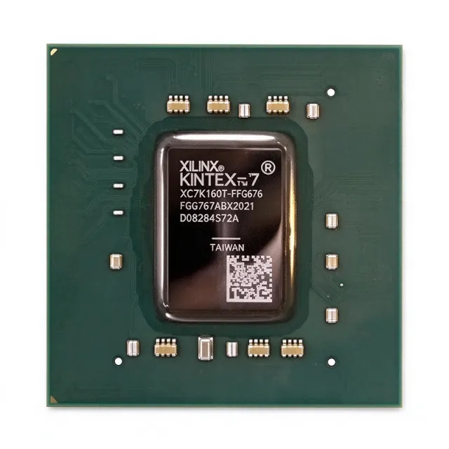
XCKU035-1FBVA900C
XCKU035-1FBVA900C - Kintex UltraScale FPGA | AMD
The AMD XCKU035-1FBVA900C is a Kintex UltraScale field-programmable gate array with 355,474 logic cells, 468 I/Os, and a 900-ball flip-chip BGA package. It operates from a nominal 0.95 V core supply, with a stated core-voltage range of 0.922 V to 0.979 V, and is built on a 20 nm process. The device is packaged as a 900-BBGA, FCBGA and targets industrial communications, high-speed processing, embedded vision, and infrastructure equipment requiring substantial parallel programmable logic.
An FPGA is a reconfigurable semiconductor in the broader category of programmable logic devices. Unlike a fixed-function ASIC, an FPGA combines configurable logic blocks, programmable I/O, memory resources, clocking, and dedicated signal-processing or serial-transceiver blocks. The Kintex UltraScale family sits above AMD’s lower-density FPGA families in logic capacity and I/O resources, making it suitable for systems that must consolidate multiple fixed functions onto one board while retaining design flexibility.
The XCKU035-1FBVA900C provides 468 I/Os, a 900-terminal package, and 355,474 logic cells. Its 0.922 V to 0.979 V core-voltage range leaves relatively little margin around the nominal 0.95 V operating point, so power delivery must account for transient behavior and package-level supply requirements. The commercial-grade ordering code is associated with a 0 °C to 85 °C operating-temperature range. Detailed resource counts, pin functions, configuration requirements, and power characteristics should be confirmed against the AMD Kintex UltraScale data sheet and package pinout files before schematic release.
Kintex UltraScale devices combine programmable logic with dedicated resources for high-speed serial connectivity, memory-intensive data processing, and clock management. That architecture allows designers to implement parallel datapaths, protocol bridges, network packet processing, embedded control, and accelerator functions in one device. The 900-ball package provides a large I/O and power-delivery interface, but its fine pitch and high ball count make clean PCB layout, plane construction, via planning, and assembly process control essential.
Typical uses include high-throughput network equipment, industrial control and test systems, video-processing infrastructure, telecommunications equipment, and embedded accelerators. The large pin count also makes the device suitable for designs requiring numerous high-speed interfaces, substantial external memory connectivity, or multiple voltage domains. Software tools, bitstreams, board support, and the selected transceiver or memory interfaces must be validated for the exact device suffix before production deployment.
The primary engineering constraint is power integrity at the 0.95 V core rail. Designers should follow the AMD recommended decoupling, package-ball, and PCB-layer guidance, provide stable power across temperature, and validate signal integrity on every high-speed interface. Configuration pins, clock inputs, resets, and dedicated transceiver pins must be assigned according to the official package pinout rather than inferred from another 900-ball device.
This product record combines the exact ordering information, package identity, core electrical conditions, resource headline, and current sourcing links with engineering guidance for power, layout, thermal, and lifecycle decisions. It also distinguishes true same-footprint family alternatives from differently packaged Kintex options so engineers can assess replacement feasibility without confusing package compatibility with functional similarity.
RFQ
संपर्क