उत्पाद (20,000+)

ES32H747XIH6U - Dual-Core ARM Cortex-M7/M4 MCU 480MHz | STMicroelectronics
ES32H747XIH6U

ES32H747XIH6U - Dual-Core ARM Cortex-M7/M4 MCU 480MHz | STMicroelectronics

The STMicroelectronics ES32H747XIH6U is a high-performance dual-core 32-bit microcontroller pairing an ARM Cortex-M7 core running up to 480 MHz with an ARM Cortex-M4 core running up to 240 MHz, integrating 2 MB of Flash and approximately 1 MB of SRAM in a 240+25-pin TFBGA (14x14 mm) package. The two cores communicate via a hardware semaphore and a shared SRAM region, allowing designers to partition real-time control on the M4 from graphics, DSP, or user-interface workloads on the M7. An MCU (microcontroller unit) is a single-chip computer that combines a CPU core, non-volatile program memory, working RAM, and a rich set of on-chip peripherals. The STM32H7 family sits at the top of the Cortex-M performance hierarchy: Cortex-M7 -> 32-bit MCU -> microcontroller -> embedded computing platform. Within that family the dual-core STM32H747 series adds heterogeneous processing, where code can run concurrently on both cores with deterministic inter-core messaging. Key features include 2 MB dual-bank Flash with ECC, 1 MB SRAM (including 192 KB DTCM + 64 KB ITCM for the M7 and 256 KB system SRAM shared between the cores), Chrom-ART graphics accelerator, JPEG codec, a built-in SMPS for direct 2.7 V–3.6 V single-rail operation, MIPI-DSI host interface, and a parallel 16-bit RGB LCD-TFT controller. Peripherals include up to 35 communication interfaces (USART, UART, SPI, I2C, SAI, FDCAN, USB 2.0 FS+HS, SDMMC), three 12-bit ADCs (3.6 MSPS), two 12-bit DACs, and crypto/hash accelerators. Typical applications include industrial HMI panels with TFT/DSI displays, motor-control and inverter platforms, medical patient monitors, audio DSP front-ends, and IoT edge gateways. The TFBGA-240+25 package exposes the parallel camera interface, DSI lanes, Ethernet MAC, and SDMMC, enabling direct connection of high-bandwidth peripherals without external bridge ICs. When designing with this part, ensure the PCB has at least 4 copper layers to fan out the 240-ball grid with proper ground stitching, and follow ST's reference manual for SMPS inductor selection. Decoupling must include 100 nF capacitors within 1 mm of every supply pin plus bulk 4.7 µF on each supply rail.

RFQ संपर्क
ESP32-P4NRW16X - Dual-Core RISC-V MCU, 16MB PSRAM | Espressif
ESP32-P4NRW16X

ESP32-P4NRW16X - Dual-Core RISC-V MCU, 16MB PSRAM | Espressif

The Espressif Systems ESP32-P4NRW16X is a 32-bit high-performance microcontroller (MCU) SoC with a RISC-V dual-core high-performance (HP) microprocessor at up to 400 MHz-class performance, a single-core low-power (LP) microprocessor, and 16 MB of in-package PSRAM (OPI/HPI) in a 10 x 10 mm QFN-104 package. A microcontroller SoC integrates a processor core, memory, and peripherals on a single chip, sitting at the top of the embedded hierarchy: MCU -> system-on-chip (SoC) -> embedded system. The ESP32-P4 family extends the ESP32 product line by removing on-chip Wi-Fi/Bluetooth radio and instead focusing on compute, memory, and display/vision peripherals, pairing naturally with Espressif companion connectivity chips such as the ESP32-C6. Key features include the HP/LP dual-system architecture, where the LP single-core RISC-V processor keeps monitoring and wake-up tasks running while the HP cores sleep; 16 MB of in-package OPI/HPI PSRAM with a 1.8 V VDD_PSRAM rail; dedicated MIPI CSI and MIPI DSI interfaces for camera input and display output; and an industrial ambient temperature range of -40 to +85 C. Technically, the ESP32-P4 is built for rich HMI, edge computing, image processing, and voice processing. The HP system contains the dual-core RISC-V microprocessor with access to large internal memory, while hardware accelerated image and voice paths offload the CPU. Espressif recommends the v3.0-or-later reference schematic and at least a 4-layer PCB for new designs, and the series is currently supplied at chip revision v3.x. Typical applications include smart display HMI panels with MIPI DSI screens, camera/vision nodes using MIPI CSI image sensors, and voice-assistant endpoints with on-device audio processing. Paired with an ESP32-C6 for Wi-Fi 6 and 802.15.4, the P4 forms the compute engine of a modern connected HMI. Design consideration: because the in-package PSRAM operates at 1.8 V (VDD_PSRAM_0/1), power-rail sequencing and the recommended 4-layer stackup with solid ground planes are critical for signal integrity on the OPI PSRAM and MIPI buses. This page synthesizes distributor pricing, drop-in alternatives within the ESP32-P4 family, and practical design notes not found in the manufacturer datasheet.

RFQ संपर्क
ESP32-P4NRW32X - Dual-Core RISC-V HMI MCU 32MB PSRAM | Espressif
ESP32-P4NRW32X

ESP32-P4NRW32X - Dual-Core RISC-V HMI MCU 32MB PSRAM | Espressif

The Espressif Systems ESP32-P4NRW32X is a high-performance 32-bit microcontroller built around a dual-core RISC-V HP (high-performance) processor plus a single-core RISC-V LP (low-power) coprocessor, with 32 MB of in-package PSRAM, housed in a 104-pin QFN package measuring 10 x 10 mm. A microcontroller (MCU) is a single integrated circuit that combines a processor core, memory, and programmable peripherals into one chip, sitting at the heart of the embedded systems hierarchy: SoC -> microcontroller -> embedded system. The ESP32-P4 is Espressif's flagship application-class MCU, positioned above the ESP32-S3 for compute-intensive embedded workloads. Key features include the HP/LP dual-system architecture that lets the LP core handle sleep-state housekeeping while the HP cores run demanding workloads, 32 MB of in-package PSRAM (the NRW32 variant) supporting large frame buffers, powerful image and voice processing capability, and rich HMI-oriented peripherals. Unlike most ESP32 family members, the ESP32-P4 focuses purely on compute; wireless connectivity is added externally via companion chips such as the ESP32-C6. Technically, the HP system contains the dual-core RISC-V processor with AI instruction extensions, an advanced memory subsystem, and integrated high-speed peripherals, while the LP system contains the single-core RISC-V low-power microprocessor. This split allows always-on voice wake-word detection or sensor polling at minimal power, waking the HP cores only when needed. Typical applications include rich Human-Machine Interfaces (HMI) with touch displays, edge computing nodes, image and camera processing pipelines, and voice processing endpoints. The large in-package PSRAM directly supports display frame buffers and AI model working sets without external memory routing. Design consideration: Espressif recommends the v3-or-later reference schematic for new designs and at least a 4-layer PCB for the 10 x 10 mm QFN-104 footprint; strapping pins must be reviewed against the ESP32-P4 datasheet before layout is frozen. This page synthesizes distributor pricing, drop-in alternatives, package guidance, and design notes not found in the manufacturer datasheet.

RFQ संपर्क
EZ80F91AZ050EG - 8-bit 50MHz eZ80 Acclaim MCU 256KB | Zilog
EZ80F91AZ050EG

EZ80F91AZ050EG - 8-bit 50MHz eZ80 Acclaim MCU 256KB | Zilog

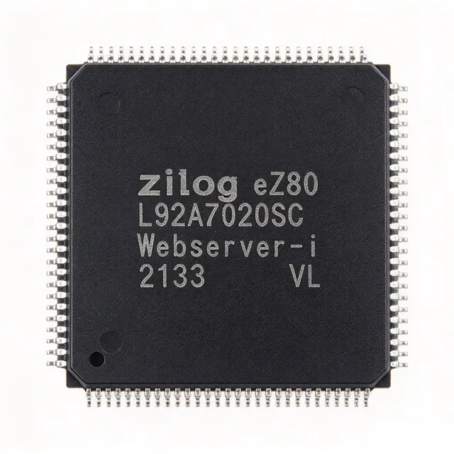
The Zilog EZ80F91AZ050EG is an 8-bit microcontroller from the eZ80 Acclaim! flash family, operating at 50 MHz with 256 KB of on-chip flash program memory and 16 KB SRAM in a 144-pin LQFP package (20x20 mm). It supports Z80-compatible 64 KB addressing or full 24-bit 16 MB linear addressing for embedded networking and industrial control. An 8-bit MCU (microcontroller unit) is a single-chip computer that integrates a CPU core, program memory (Flash/ROM), working memory (SRAM), and peripherals on one die. The eZ80 is a CISC (Complex Instruction Set Computer) core — a Z80-compatible architecture that retains legacy object code while extending to 24-bit linear addressing, placing it in the hierarchy: 8-bit MCU -> microcontroller -> embedded processor -> semiconductor IC. Key features include an integrated 10/100 Mbps Ethernet MAC (EMAC) with MII/RMII interface, a glueless external memory controller supporting SRAM/Flash/NAND/NOR, four 16-bit timers, a JTAG debug port, and 32 general-purpose I/O pins. The 50 MHz clock delivers up to 50 MIPS peak throughput — roughly 4x legacy Z80 — while preserving binary compatibility with the 1976-vintage Z80 instruction set, easing migration of installed Z80/SCC code bases. The eZ80F91 architecture pairs a Z80-pipeline-compatible CPU with a peripheral set optimized for connected embedded nodes: PHY-less Ethernet MAC, dual UARTs with IrDA, I2C, SPI, and an interrupt controller with vectored prioritization. On-chip voltage regulation supports a 3.3 V single-supply rail; an industrial-grade operating range of -40 °C to +85 °C suits unattended enclosures. Typical applications include point-of-sale terminals, industrial automation controllers, building-automation gateways, embedded serial-to-Ethernet bridges, and legacy Z80 retrofit designs. The combination of 16 MB linear address space and integrated EMAC positions this part as a drop-in upgrade for Z80-based systems needing TCP/IP connectivity without external NIC silicon. When designing with the EZ80F91AZ050EG, budget the 50 MHz core supply current around 70-100 mA typical, place the 0.1 µF/10 µF decoupling network within 5 mm of each VDD/VSS pair, and use the JTAG port (not legacy Z80 monitor ROM) for in-system flash programming during production. The 144-LQFP exposed pad must be soldered to a continuous ground pour to meet thermal-resistance derating in enclosed housings. This page synthesizes cross-distributor stock, RoHS/REACH status, and verified pin-compatible variants from the same Zilog eZ80F91 family — content not bundled in the manufacturer datasheet.

RFQ संपर्क
EZ80F91AZ050SG - 50MHz 256KB Flash eZ80 MCU | Zilog | 144-LQFP
EZ80F91AZ050SG

EZ80F91AZ050SG - 50MHz 256KB Flash eZ80 MCU | Zilog | 144-LQFP

The Zilog EZ80F91AZ050SG is an 8-bit eZ80 Acclaim! flash microcontroller running at 50 MHz with 256 KB of on-chip flash and 16 KB SRAM, housed in a 144-pin LQFP (20x20 mm) package. It supports both 24-bit linear addressing up to 16 MB of external memory and the legacy Z80-compatible 64 KB addressing mode, making it a drop-in upgrade path for classic Z80/HD64180 designs while retaining object-code compatibility. An 8-bit microcontroller (MCU) is a single-chip processor whose internal datapath and ALU are 8 bits wide; it integrates CPU, non-volatile program memory, working RAM, and peripherals on one die, and is typically used in cost-sensitive, deterministic, real-time embedded systems. The eZ80 Acclaim! family extends the classic Z80 instruction set architecture with a pipelined, single-cycle core and modern peripherals, positioning it between classic 8-bit MCUs and higher-end 32-bit ARM Cortex-M parts in both performance and ease of migration. Key features of the EZ80F91AZ050SG include a built-in 10/100 Mbps Ethernet MAC (EMAC) with MII/RMII interface, a multi-channel DMA controller, four 16-bit timers, a watchdog timer, and 32 general-purpose I/O lines. A peripheral set with USB 2.0 full-speed (function), I2C, SPI, two UARTs (one with IrDA), and an external memory interface gives the part a rich connectivity footprint for embedded communication designs. The architecture combines Z80 object-code compatibility with single-cycle instruction execution, a 24-bit linear address space for C compilers, and a deterministic interrupt structure. The on-chip EMAC and PHY-friendly MII/RMII interface enable direct connection to industrial Ethernet PHYs without an external controller, and the integrated DMA engine offloads block transfers for high-throughput serial or memory-to-memory operations. Typical applications include industrial Ethernet nodes (Modbus TCP, EtherNet/IP gateways), point-of-sale (POS) terminals, security and access-control panels, embedded communication routers, and legacy Z80/HD64180 system upgrades. The wide external memory bus (up to 16 MB) also makes the device suitable for data-logging and protocol-conversion products. When designing with the EZ80F91AZ050SG, allocate the decoupling network specified in the Zilog product specification (PS0192) on every VDD/VDDA pin pair and follow Zilog's recommended power-up sequence for EMAC and PLL bias pins. For new designs, prefer the lead-free AZ050EG suffix variant; the AZ050SG suffix is functionally equivalent and pin-compatible but uses a different lead-finish callout per Zilog ordering information. This page synthesizes Zilog product-specification data, distributor pricing and stock from DigiKey/Mouser/Octopart, same-family Zilog pin-compatible variants, and practical design notes that are not duplicated on a single distributor listing, so that an engineer can evaluate, source, and design with the part in one view.

RFQ संपर्क
EZ80F91GAZ0BEG - 50MHz 8-bit eZ80 MCU 256KB Flash | Zilog
EZ80F91GAZ0BEG

EZ80F91GAZ0BEG - 50MHz 8-bit eZ80 MCU 256KB Flash | Zilog

The Zilog EZ80F91GAZ0BEG is a high-performance 8-bit eZ80Acclaim! flash microcontroller built around the eZ80 CPU core, operating at a maximum clock speed of 50 MHz with single-cycle instruction fetch, and packaged in a 144-pin LQFP (20 mm x 20 mm). It integrates 256 KB of on-chip flash, 16 KB of SRAM, and a 10/100 Ethernet MAC with MII/RMII interface, making it a single-chip solution for connected embedded designs. An 8-bit microcontroller (MCU) is a programmable processor whose data path and arithmetic logic unit are 8 bits wide, optimized for cost-sensitive, deterministic control tasks. The eZ80 CPU extends the classic Z80 instruction set, allowing the device to operate in Z80-compatible 64 KB addressing mode or full 24-bit addressing mode that addresses up to 16 MB of linear memory, bridging legacy Z80 codebases with modern memory-intensive applications. The EZ80F91 family sits within Zilog's eZ80Acclaim! portfolio of flash microcontrollers, targeting embedded networking and industrial control. Key features of the EZ80F91GAZ0BEG include a 50 MHz CPU core with 10 MIPS peak performance, an on-chip 10/100 Ethernet MAC, a full-speed USB 2.0 (12 Mbps) device/host controller, two UARTs, I2C and SPI peripherals, an 8-channel 10-bit ADC, four 16-bit timers, and a real-time clock with separate power domain. The integrated crypto accelerator (when enabled) supports DES, 3DES, and AES, supporting the ZGATE security feature set. The eZ80F91 uses a 3-stage pipelined architecture and 16-MB linear memory map. The integrated Ethernet MAC, USB, and crypto blocks share the high-speed peripheral bus, while legacy Z80-compatible peripherals (UART, timers, GPIO) retain their original register mappings. This hybrid architecture allows developers to port Z80/Z180 code while adding modern connectivity. Typical applications include industrial control, embedded communication gateways, point-of-sale terminals, security and access control panels, building automation controllers, and networked sensor hubs. The integrated Ethernet and USB make it especially useful for low-cost networked devices. When designing with the EZ80F91GAZ0BEG, ensure the 3.0V to 3.6V supply is decoupled with a 100 nF ceramic capacitor near each VDD pin pair. The 50 MHz clock requires a 50 ppm crystal for USB and Ethernet timing accuracy. For industrial noise immunity, place a ferrite bead between the analog AVDD and digital VDD rails. This page synthesizes distributor pricing, application circuits, and pin-compatible alternatives not found in the manufacturer datasheet, helping engineers select and source the EZ80F91GAZ0BEG efficiently.

RFQ संपर्क
EZ80L92AZ020SG - eZ80 8-Bit MCU 20MHz ROMless LQFP-100 | Zilog
EZ80L92AZ020SG

EZ80L92AZ020SG - eZ80 8-Bit MCU 20MHz ROMless LQFP-100 | Zilog

The Zilog EZ80L92AZ020SG is an 8-bit eZ80 Acclaim! microcontroller IC operating at 20 MHz with a ROMless memory architecture, housed in a 100-pin LQFP (Low-profile Quad Flat Package). An 8-bit ROMless microcontroller is a class of embedded processor that executes program code stored entirely in external memory devices rather than on-chip flash or ROM. The ROMless approach gives system designers freedom to select external flash size, update firmware in the field, and build modular memory subsystems. The eZ80 core is a Z80-compatible architecture that executes instructions roughly 3x faster than a classic Z80 at the same clock frequency, while remaining binary-compatible with the vast Z80 software ecosystem. Key features of the EZ80L92AZ020SG include the 20 MHz eZ80 core, 24-bit linear address space supporting up to 16 MB of external memory, two UARTs with IrDA support, I2C and SPI serial interfaces, and six 16-bit timers. The device is lead-free and qualified for standard commercial temperature operation. Technically, the eZ80L92 integrates a Z80-compatible CPU core with a rich on-chip peripheral set and an external bus controller, enabling designs that mix legacy Z80 code with modern peripherals. The wide external memory interface allows glueless connection of SRAM, flash, and Ethernet companion devices from the eZ80 Acclaim! family ecosystem. Typical applications include industrial control systems, legacy Z80 equipment upgrades, Ethernet-connected embedded modules (such as the eZ80L92 module reference design), data loggers, and communication interface bridges. When designing with this ROMless device, budget external flash access wait states and lay out the address/data bus with controlled trace lengths for reliable 20 MHz operation. This page synthesizes distributor pricing, same-package drop-in alternatives, and practical design notes not found in the manufacturer datasheet alone.

USD $14.77 स्टॉक में
F-XC866-4FRI - 8-Bit XC800 MCU 16KB Flash 26.7MHz | Infineon
F-XC866-4FRI

F-XC866-4FRI - 8-Bit XC800 MCU 16KB Flash 26.7MHz | Infineon

The Infineon F-XC866-4FRI is an 8-bit single-chip microcontroller based on the high-performance XC800 CISC core with on-chip FLASH memory and integrated peripherals. The device operates at up to 26.7 MHz CPU clock, integrates 16 KB on-chip program FLASH and 768 B RAM, and is housed in a PG-TSSOP-38 surface-mount package. It combines a powerful 8051-compatible instruction set with embedded peripherals tuned for cost-sensitive industrial and automotive sensor applications. An 8-bit microcontroller (MCU) is a programmable logic device that integrates a CPU, non-volatile program memory, volatile data memory, and peripheral blocks onto a single silicon die. Within the broader semiconductor taxonomy, an 8-bit MCU is a sub-class of microcontroller, itself a sub-class of embedded processor, which falls under the Integrated Circuits hierarchy. The Infineon XC800 family specifically targets applications requiring deterministic real-time response, on-chip analog signal conditioning, and high immunity to automotive electromagnetic interference. Key features of the F-XC866-4FRI include a 5 V single-voltage supply with on-chip voltage regulator and on-chip oscillator, embedded ADC for analog signal acquisition, capture/compare units (CCU) for PWM generation, and a MultiCAN node for automotive network interfacing. The on-chip voltage regulator enables operation from a single 5 V supply, simplifying PCB power design, while the embedded oscillator eliminates the external crystal in many cost-driven applications. These features collectively support sensor signal acquisition, actuator control, and LIN-bus networked nodes. Architecturally, the F-XC866-4FRI employs a Harvard-style memory organization with separate program and data paths. The on-chip FLASH supports in-system programming (ISP) and in-application programming (IAP) for field firmware updates. The MultiCAN module provides hardware-accelerated CAN 2.0B frame handling, offloading the CPU and improving real-time responsiveness. The capture/compare and PWM units operate independently of the CPU, supporting high-resolution timing without software overhead. Typical applications include automotive body electronics such as door modules, seat controllers, and lighting controllers; industrial sensor signal conditioning; small motor control in HVAC dampers and pumps; and LIN-bus slave nodes communicating with a central body controller. The on-chip oscillator with PLL multiplication allows flexible clock generation without external crystals. When designing with the F-XC866-4FRI, ensure the supply decoupling follows Infineon reference design guidelines - a 100 nF ceramic capacitor close to each VDD pin plus a bulk tantalum or aluminum-polymer capacitor on the 5 V rail. The MultiCAN bus lines require external ESD protection and common-mode chokes for automotive EMC compliance, and unused GPIO pins should be configured as outputs with defined levels to minimize current leakage. This page synthesizes distributor pricing, drop-in alternatives, and practical design notes not found in the manufacturer datasheet, providing an engineer-focused overview optimized for sourcing, replacement, and design decisions.

RFQ संपर्क
F280023PMSR - C2000 32-bit MCU, 100MHz, 64KB Flash, 64-LQFP | Texas Instruments
F280023PMSR

F280023PMSR - C2000 32-bit MCU, 100MHz, 64KB Flash, 64-LQFP | Texas Instruments

The Texas Instruments F280023PMSR is a C2000™ 32-bit real-time microcontroller from the F28002x family, featuring a C28x CPU core with FPU and TMU running at 100 MHz, paired with 64 KB (32K x 16) of flash memory and packaged in a 64-pin LQFP (PM) measuring 10x10 mm. The device integrates a single-precision floating-point unit and a trigonometric math unit, making it purpose-built for control-loop math in power-conversion and motor-drive applications. Per the LCSC distributor listing, this MPN carries the 'S' temperature grade, supporting -40°C to 125°C junction temperature in a natural convection environment. A C2000 microcontroller is a 32-bit MCU family engineered specifically for real-time control. In the broader taxonomy, the F280023PMSR sits as: microcontroller -> embedded MCU -> 32-bit MCU -> real-time control MCU -> C2000 family -> F28002x sub-family. Unlike general-purpose MCUs that prioritize connectivity or low power, C2000 devices focus on deterministic interrupt latency and high-resolution PWM generation, which are foundational for digital control of switches, motors, and power converters. Key features include the 100 MHz C28x core with hardware FPU/TMU for single-cycle trigonometric math, 64 KB flash, integrated control peripherals (ePWM, eCAP, eQEP), analog comparators and ADCs, plus InstaSPIN-FOC library compatibility. The device's FPU/TMU offloads math-intensive routines such as Park/Clarke transforms, freeing the CPU for application logic. The 64-LQFP package offers generous GPIO and a generous PCB thermal pad footprint for cost-sensitive designs. Architecturally, the F28002x combines the legacy C28x DSP-style core with a C28x+CLA-style bus matrix and a tightly-coupled control-law accelerator option in higher SKUs. The FPU executes single-precision IEEE-754 arithmetic in hardware, while the TMU accelerates sin, cos, arctan, and square-root operations used in field-oriented control (FOC) firmware. Typical applications include solar inverters, industrial motor drives (BLDC/PMSM), digital power supplies, traction inverters, and LED lighting drivers. The integrated PWM and ADC peripherals make it a strong fit for any closed-loop digital control system that demands deterministic sub-microsecond response. When designing with this part, ensure your linker script reserves the correct flash wait-state configuration for 100 MHz operation, and review the boot-ROM GPIO multiplexing table before laying out the PCB. This page synthesizes distributor pricing, same-family F28002x drop-in alternatives, and practical design notes not found in the manufacturer datasheet alone.

RFQ संपर्क
F280045PMSR - C2000 32-bit MCU, 100MHz, 256KB Flash | TI
F280045PMSR

F280045PMSR - C2000 32-bit MCU, 100MHz, 256KB Flash | TI

The Texas Instruments F280045PMSR is a C2000™ 32-bit Piccolo™ microcontroller with a 100 MHz C28x CPU core, 256 KB of on-chip flash, and a 64-pin LQFP (PM) package measuring 10x10 mm. It integrates a single-precision floating-point unit (FPU) and a Trigonometric Math Unit (TMU) for accelerated math operations commonly required in real-time control loops. A microcontroller (MCU) is a programmable processor that integrates a CPU core, memory (Flash and RAM), and peripherals into a single silicon die. The C2000 family sits inside the broader microcontroller taxonomy as MCU -> 32-bit MCU -> DSP-enhanced MCU -> real-time control MCU, and is purpose-built for digital power conversion, motor control, and signal-conditioning applications where deterministic, sub-microsecond interrupt response is required. Key features include 256 KB (256K x 8) of flash, 100 KB of RAM, fourteen 12-bit ADC channels, two 12-bit DAC outputs, three on-chip programmable gain amplifiers (PGAs), and a Sigma-Delta Filter Module (SDFM) for isolated current/voltage sensing. Communication peripherals include SPI, SCI/UART, I2C, CAN, and LIN. The 1.14 V to 1.32 V core supply is generated internally from a 3.3 V rail via an integrated voltage regulator. The architecture pairs a Harvard-style bus with a tightly coupled control-law accelerator (CLA) and the FPU/TMU pair, executing trigonometric and matrix operations in hardware. This reduces software loop latency versus a software-emulated math approach, allowing higher switching frequencies in digital power supplies. Typical applications include digital totem-pole PFC converters, solar inverters, server/telecom SMPS, industrial motor drives, traction inverters, EV charging stations, and battery management systems. The SDFM and PGA blocks particularly benefit isolated shunt-based current sensing in high-voltage systems. When designing with this device, ensure the 3.3 V supply is decoupled with at least one 1 µF and one 100 nF ceramic capacitor near each VDDS pin, and follow TI's SPRS942 layout guidelines for the LQFP PM package to keep digital return currents out of the analog ground domain. This page synthesizes distributor pricing, drop-in package-compatible alternatives, and practical design notes that are not found in the manufacturer datasheet alone.

RFQ संपर्क
F280049CPZQR - 32-bit C2000 MCU 100MHz 256KB Flash 100-LQFP | TI
F280049CPZQR

F280049CPZQR - 32-bit C2000 MCU 100MHz 256KB Flash 100-LQFP | TI

The Texas Instruments F280049CPZQR is a 32-bit C2000 Piccolo-class automotive-grade microcontroller (MCU) running at 100 MHz with 256 KB of integrated Flash, 100 KB of SRAM, and a C28x CPU core augmented by a single-precision FPU, TMU accelerator, and a programmable Control Law Accelerator (CLA). The device is housed in a 100-pin LQFP (PZ) package measuring 14 mm x 14 mm with 0.5 mm lead pitch. What is a C2000 Piccolo MCU? The C2000 family is Texas Instruments' real-time microcontroller platform optimized for closed-loop digital control of power conversion, motor drive, and lighting systems. Piccolo is the cost- and feature-optimized sub-family within C2000, sitting below the Delfino performance line but above the value-oriented F28002x line. The hierarchy is: C28x core -> C2000 real-time MCU -> digital signal controller -> embedded processor. Key features of the F280049CPZQR include four 12-bit analog-to-digital converters (ADCs) for high-speed sensing, two 12-bit DACs for analog reference generation, three on-chip programmable gain amplifiers (PGAs), sigma-delta filter (SDFM) channels for isolated current sensing, four configurable logic blocks (CLBs) for hardware customization, and a rich communications peripheral set including CAN-FD, SPI, I2C, UART, and LIN. The supply voltage range of 1.14 V to 1.32 V for the core and 3.3 V for the I/O ring makes it compatible with industrial and automotive power trees. Architecturally, the F280049C variant differs from the F280049 base device by adding CLB logic. The C28x core runs at 100 MHz (10 ns cycle time), delivering 100 MIPS with deterministic interrupt latency under 25 cycles, which is critical for digital power control loops operating at sub-microsecond periods. The integrated CLA offloads time-critical control tasks from the CPU, freeing it for higher-level supervisory functions, communications, and fault handling. Typical applications include on-board chargers (OBC) and DC-DC converters for electric vehicles, traction inverters, solar micro-inverters, telecom rectifiers, server power-supply units (PSU), digital LED drivers, and industrial motor-control servo drives. The wide operating temperature range of -40 C to +125 C and AEC-Q100 qualification make the part suitable for under-hood automotive environments. Designers should size local decoupling per the datasheet (typically 1 x 100 nF + 1 x 4.7 uF per VDD pin pair) and follow the PCB layout recommendations in the F28004x hardware-design guide. Because this is a 0.5 mm-pitch LQFP, hand-rework is feasible - unlike BGAs in the same family - which simplifies prototype bring-up and field rework. This page consolidates distributor pricing, verified drop-in alternatives, application notes, and design tips not found in the manufacturer datasheet alone.

RFQ संपर्क
F280049CPZS - 100MHz C28x MCU 256KB Flash LQFP-100 | TI
F280049CPZS

F280049CPZS - 100MHz C28x MCU 256KB Flash LQFP-100 | TI

The Texas Instruments F280049CPZS is a C2000™ 32-bit Piccolo microcontroller built on the C28x core, running at 100 MHz with an integrated single-precision FPU, Trigonometric Math Unit (TMU), and Control Law Accelerator (CLA), packaged in a 100-pin LQFP (PZ) measuring 14x14 mm. It integrates 256 KB of flash, 100 KB of RAM, an InstaSPIN-FOC motor-control library, Configurable Logic Block (CLB), programmable gain amplifiers (PGAs), and Sigma-Delta Filter Module (SDFM) peripherals on-chip. A C2000 Piccolo microcontroller is a real-time control MCU in TI's C2000 family, architected for high-performance digital control loops in power electronics and motor drives. The C28x core executes deterministic control code at fixed cycle counts; the on-chip FPU accelerates floating-point math while the TMU offloads sin/cos/atan/division, all critical for field-oriented control. C2000 MCUs occupy the "real-time MCU" stratum in TI's MCU taxonomy (C2000 > TMS320 > 32-bit MCU > microcontroller > embedded processing). The device supports 3.0-3.6 V I/O and 1.14-1.32 V core supply via internal LDO. It includes 21 channels of 12-bit ADC, two 12-bit DACs, multiple high-resolution PWM modules with valley switching, plus CAN-FD, SPI, UART, I2C, and USB connectivity. On-chip PGAs with up to 12x gain enable direct current-shunt feedback without external amplifiers in motor drives. F280049CPZS targets digital power converters (totem-pole PFC, LLC, phase-shifted full-bridge), industrial motor drives (PMSM, BLDC, ACIM, SR), servo amplifiers, solar inverters, and on-board EV chargers. The InstaSPIN-FOC library identifies motor parameters without rotary sensors in under 2 minutes. Designers should allocate 4-layer PCB with a solid ground pour under the LQFP-100 thermal pad. For SVM at 100 kHz, ensure DC-DC supply ripple is below 50 mVpp. The CLB allows custom logic on-chip, eliminating external CPLDs in many fault-handling circuits. This page consolidates datasheet specifications, drop-in alternatives, distributor stock, and design notes that complement the manufacturer datasheet with selection-oriented engineering context.

RFQ संपर्क
F28027PTT - 60MHz C28x Piccolo MCU, 64KB Flash | Texas Instruments
F28027PTT

F28027PTT - 60MHz C28x Piccolo MCU, 64KB Flash | Texas Instruments

The Texas Instruments F28027PTT (also known as TMS320F28027PTT) is a 32-bit C2000 Piccolo microcontroller built around the C28x core, operating at up to 60 MHz. It features 64KB (32K x 16) of flash memory and is housed in a 48-pin LQFP (PT) package measuring 7x7 mm. This device is designed for real-time control applications, offering a high level of analog integration and an internal voltage regulator for single-rail operation. A microcontroller (MCU) is a compact integrated circuit that combines a processor core, memory, and programmable input/output peripherals on a single chip. The C28x core is a 32-bit fixed-point DSP-optimized architecture from Texas Instruments, specifically engineered for real-time control tasks. It sits within the C2000 family, which is a subset of microcontrollers tailored for industrial and automotive control systems, such as motor drives, power conversion, and digital power supplies. The C28x core excels at executing control algorithms with high precision and low latency, making it a preferred choice for closed-loop systems. Key features of the F28027PTT include a 60 MHz clock speed, 64KB flash memory, and a rich set of control peripherals. It integrates a 12-bit ADC, multiple PWM channels, and communication interfaces like SPI, SCI (UART), and I2C. The device operates over a temperature range of -40°C to 105°C, making it suitable for harsh environments. The internal voltage regulator simplifies power supply design, allowing operation from a single 3.3V rail. Technically, the F28027PTT leverages the C28x core's Harvard architecture, which enables simultaneous instruction and data access, improving throughput. The flash memory supports on-chip programming, facilitating firmware updates in the field. The device also includes a boot ROM with factory-programmed bootloader routines, enabling flexible boot options from various interfaces. The analog-to-digital converter (ADC) offers 12-bit resolution with multiple sample-and-hold channels, crucial for precise sensor measurements in control loops. Typical applications include white goods (such as washing machines and refrigerators), switched-mode power supplies (SMPS), and DC-DC multiple-output power supplies. The F28027PTT's high-performance C28x core and integrated peripherals make it ideal for implementing complex control algorithms like field-oriented control (FOC) for motors and digital power conversion. Its low pin count and small package footprint also suit space-constrained designs. When designing with this device, ensure proper decoupling of the power supply pins and consider the thermal characteristics of the LQFP package. The internal voltage regulator requires an external capacitor for stability. Additionally, the ADC reference pins should be filtered to minimize noise, as this directly impacts measurement accuracy in control applications.

RFQ संपर्क
F29H859TU-Q1 - Automotive C2000 64-bit MCU | Texas Instruments
F29H859TU-Q1

F29H859TU-Q1 - Automotive C2000 64-bit MCU | Texas Instruments

The Texas Instruments F29H859TU-Q1 is an automotive-grade C2000 real-time microcontroller featuring a 64-bit C29x CPU running at 200MHz with triple-core architecture and lockstep capability. It provides 4MB of flash memory and is designed for functional safety compliance in power electronics, motor control, and GaN/SiC-based applications. The C2000 family is a well-known series of ultra-low-latency MCUs optimized for real-time control. The F29H859TU-Q1 belongs to the F29H85x sub-family, which leverages the next-generation C29 CPU core to enable high power density and high switching frequency operation. This MCU is specifically qualified for automotive environments (Q1 suffix), meeting the stringent reliability and AEC-Q100 standards required in vehicles. Key features of the F29H859TU-Q1 include a triple-core 200MHz C29x CPU with lockstep mode for enhanced safety, 4MB flash memory, and functional safety compliance. The architecture supports advanced real-time control loops, making it suitable for applications like DC-DC converters, traction inverters, on-board chargers, and solar inverters. The F29H859TU-Q1 is available in a BGA package, which is the only practical packaging option for this high pin-count MCU as confirmed by TI support. The device is designed for surface mount assembly and operates across automotive temperature ranges, enabling compact and robust system designs. Typical applications include digital power supply control, motor control for electric vehicles, renewable energy inverters, and industrial automation systems. The high-performance CPU and large flash memory allow for complex algorithms and firmware updates, while the functional safety features ensure reliable operation in safety-critical systems. When designing with the F29H859TU-Q1, engineers should consider adequate thermal management and decoupling for high-speed digital switching. The C29x architecture requires careful attention to power supply stability and PCB layout to maximize performance and safety.

RFQ संपर्क
F29P329SM-Q1 - 200MHz C29 Auto MCU | Texas Instruments
F29P329SM-Q1

F29P329SM-Q1 - 200MHz C29 Auto MCU | Texas Instruments

The Texas Instruments F29P329SM-Q1 is an automotive-grade 64-bit C2000 real-time microcontroller featuring the next-generation C29 CPU running at 200 MHz. It integrates 2MB of flash memory and supports lockstep operation for functional safety compliance, making it suitable for ASIL-D / SIL-3 applications. The device comes in a 100-pin PZS package and operates over -40°C to +125°C. What is a C2000 real-time microcontroller? The C2000 family is a series of MCUs designed for real-time control applications such as motor control, power conversion, and digital power supplies. These MCUs feature a highly efficient CPU with low latency, integrated analog peripherals (ADCs, DACs, comparators), and enhanced PWM modules, enabling precise control loops. The C29 CPU is the latest generation, offering higher performance and advanced safety features. Key features include 200MHz operation, 2MB flash, lockstep with error detection, functional safety compliance (ISO 26262), and automotive AEC-Q100 qualification. The C29 core is a 64-bit architecture with 128-bit data paths, providing faster single-cycle access to memory. The device supports multiple communication interfaces such as CAN, UART, SPI, and I2C, though exact counts are not available from the provided data. Typical applications include automotive motor control (e.g., traction inverters), digital power supplies (e.g., LLC converters), vehicle electrification (battery management), industrial drives, and renewable energy inverters. The 200MHz clock and advanced PWM capabilities ensure high-precision control loops. When designing with this MCU, pay attention to power supply decoupling and thermal management. The 200MHz core can dissipate significant power; use multiple VDD pins with ceramic capacitors and consider thermal vias under the exposed pad. Also, use the lockstep fail-safe features to implement safe shutdown paths.

RFQ संपर्क
FF8062701084002 - Celeron B730 1.80GHz Mobile CPU | Intel
FF8062701084002

FF8062701084002 - Celeron B730 1.80GHz Mobile CPU | Intel

The Intel FF8062701084002 is the OEM packaging code for the Mobile Intel Celeron Processor B730, a single-core 1.80 GHz CPU built on the Sandy Bridge microarchitecture and packaged in a Socket G2 (FCPGA10) form factor. The part runs at 1.80 GHz base frequency, integrates 256 KB of L2 cache and a shared 1.5 MB Intel Smart Cache (L3), supports a 5 GT/s DMI link to the Mobile Intel HM65/HM70 Express chipset, and has a 35 W TDP designed for notebook platforms. Background - What is a mobile Celeron processor? The Intel Celeron line is a value-tier x86 CPU family positioned below the Core i3/i5/i7 series in Intel's mobile product stack. A Celeron Dual-Core B730 belongs to the Sandy Bridge (2nd-generation Core) family and uses the same 32 nm process as mainstream Core parts, but with reduced L3 cache and a single active core (the "Dual-Core" suffix reflects the dual-core silicon die with one core enabled). This places the B730 in the broader hierarchy: CPU -> x86 processor -> mobile Celeron -> Sandy Bridge -> Intel mobile value-segment family. Key features include a 1.80 GHz core frequency, 2.5 GT/s on-die interconnect, integrated Intel HD Graphics (Graphics 2000-class) running at 650-1000 MHz, SSE4.x instruction set support, Intel 64 architecture, and Execute Disable Bit for security. The 35 W TDP allows thin-and-light notebook designs without active cooling upgrades. Virtualization (VT-x) is supported for entry-level server and desktop-virtualization workloads. From an architectural standpoint, the B730 implements a single Sandy Bridge core with the legacy ring-topology L3 cache, dual-channel DDR3 memory controller (up to DDR3-1333), and a flexible DMI 2.0 link to the PCH. The shared 1.5 MB L3 cache, while smaller than the 3-8 MB found on Core parts, is sufficient for entry-level office workloads and basic multimedia playback. Hyper-Threading is disabled on the Celeron B730 (1 core / 2 threads vs. the dual-core B8xx SKUs), and Turbo Boost is also disabled, keeping the part at a fixed 1.80 GHz. Typical applications include low-cost business notebooks, education/1:1 classroom laptops, entry-level consumer laptops, point-of-sale terminals, and thin-client devices. The B730 is also used in legacy industrial PCs and embedded HMIs where Socket G2 motherboards are already deployed. Design considerations: pairing the B730 with a Mobile Intel HM65 or HM70 chipset PCH is required because of the DMI 2.0 host interface. Memory must be DDR3 SO-DIMM (1.5 V) in dual-channel configuration for maximum bandwidth; mixing densities will fall back to single-channel. The OEM tray part (FF8062701084002) is intended for system integrators - retail boxed equivalents carry a different SSPEC code. This page synthesizes OEM packaging identification, key specifications, real distributor listings, drop-in alternatives, and practical design notes not found in the manufacturer datasheet.

RFQ संपर्क
FS32K116LAT0MFMT - S32K116 48MHz 128KB Flash MCU | NXP
FS32K116LAT0MFMT

FS32K116LAT0MFMT - S32K116 48MHz 128KB Flash MCU | NXP

The NXP Semiconductors FS32K116LAT0MFMT is an ARM Cortex-M0+ 32-bit automotive microcontroller from the S32K1 family, operating at 48 MHz with 128 KB of Flash memory and housed in a 32-pin HVQFN (5x5 mm) package. It integrates FlexCAN with CAN FD support, hardware cryptographic security (CSEc), and FlexIO for flexible peripheral emulation. A microcontroller (MCU) is a single-chip computer containing a processor core, program memory (Flash), working memory (RAM), and a rich set of on-chip peripherals. In the automotive electronic control unit (ECU) hierarchy, the S32K116 sits at the entry level of the S32K1 scalable family that targets general-purpose automotive and high-reliability industrial applications compliant with ISO 26262 up to ASIL B. Its Cortex-M0+ core is optimized for deterministic real-time control at very low power. Key features include 128 KB Flash, 16 KB (or up to 17 KB per Mouser summary) SRAM, a 2.7 V to 5.5 V supply range suitable for direct automotive 12 V battery regulation, low-power run/stop/vlpr/vlps modes, and an integrated CAN FD controller for modern automotive networking. The 32-HVQFN package (5x5 mm) is a thermally enhanced leadless QFN that supports reflow soldering and minimizes PCB footprint. The device is part of NXP's FunSafeTI-equivalent SafeAssure program and is qualified to AEC-Q100. The S32K116 uses the Cortex-M0+ Von Neumann core with a 3-stage pipeline and NVIC interrupt controller. It incorporates a bandgap-based analog block supporting ADC and comparators, FlexIO for emulating UART/SPI/I2C, and an on-chip CSEc cryptographic engine (AES-128) for secure boot and secure communication. The combination of Cortex-M0+ simplicity with automotive peripherals makes the architecture ideal for deterministic body and chassis control. Typical applications include automotive body controllers, CAN-FD gateway nodes, BCM (body control modules), lighting/ECL controllers, HVAC blowers, seat/window control units, and industrial PLCs requiring AEC-Q100 reliability. The 128 KB Flash tier targets applications that outgrow lower-end S32K11x parts but do not need the larger memories of S32K14x. When designing with this part, allocate PCB copper area under the exposed pad for thermal relief (although at typical automotive temperatures and lower clock peripherals the dissipation is modest). Confirm the CAN FD bit-rate and bus load against the FlexCAN reference manual; use NXP's S32 Design Studio and the SDK for the configuration framework. Check the latest errata before committing to a PCB revision. This page synthesizes distributor pricing, parametric comparison with same-family alternatives, and design notes sourced from NXP's S32K1xx datasheets - context not present on a single distributor page.

RFQ संपर्क
FS32K118LAT0MLFT - 256KB Flash Cortex-M0+ 48MHz MCU | NXP
FS32K118LAT0MLFT

FS32K118LAT0MLFT - 256KB Flash Cortex-M0+ 48MHz MCU | NXP

The NXP Semiconductors FS32K118LAT0MLFT is an ARM Cortex-M0+ 32-bit automotive microcontroller from the S32K1 family, integrating 256 KB of Flash and 25 KB of RAM, running at up to 48 MHz, and housed in a 48-pin LQFP (7x7 mm) package rated for 3.3 V / 5 V operation. It is part of the general-purpose S32K MCU lineup and is AEC-Q100 qualified for automotive use. A microcontroller (MCU) is a single-chip computer that integrates a CPU core, program and data memory, peripherals, and I/O. The Cortex-M0+ core implements the Armv6-M architecture with a 2-stage pipeline and is tailored for deterministic, low-power embedded control. S32K1 family MCUs sit in the broader hierarchy: Cortex-M0+ -> 32-bit MCU -> automotive MCU -> semiconductor, and are widely adopted in body electronics and chassis applications. Key features include a CAN FD controller for high-bandwidth in-vehicle networking, FlexIO for emulating additional UART/SPI/I2C/IIS interfaces, an HSE security engine supporting CSEc for secure boot and key storage, low-power run and standby modes, and a 12-bit ADC with up to 16 channels plus a comparator and FTM timers for motor and PWM control. The 48 MHz maximum core frequency provides ample headroom for sensor fusion and protocol stacks. Technically, the S32K118 die uses an embedded Flash controller with ECC, hardware cryptographic acceleration in the HSE block (AES, RSA, ECC), and a sophisticated clock tree supporting PLL, FLL, and external crystal references. Functional safety features target ISO 26262 up to ASIL B, with hardware watchdog, ECC on SRAM, and a fault collection unit. Typical applications include automotive body control modules, HVAC controllers, seat and mirror modules, lighting ECUs, basic gateway nodes with CAN FD, industrial sensor hubs, and any low-power 32-bit replacement for legacy 8/16-bit MCUs that still requires CAN, security, and AEC-Q100 compliance. When designing with this part, ensure the 5 V tolerant I/O rails do not exceed 5.5 V and provide bulk decoupling near VDDA. Place the 8 MHz external crystal within 5 mm of XTAL pins and route HSE_FUSE power correctly to enable secure boot. This page combines distributor pricing, drop-in S32K1 alternatives, and S32K118-specific design notes not available on the manufacturer summary page.

RFQ संपर्क
FS32K142HAT0MLHT - S32K142 ARM Cortex-M4F 80MHz MCU | NXP
FS32K142HAT0MLHT

FS32K142HAT0MLHT - S32K142 ARM Cortex-M4F 80MHz MCU | NXP

The NXP FS32K142HAT0MLHT is an ARM Cortex-M4F 32-bit microcontroller from the S32K1 family, featuring an 80 MHz core, 256 KB of Flash, and housed in a 64-pin LQFP (10x10 mm) package. It is part of NXP's S32K1xx family designed for general-purpose automotive and high-reliability industrial applications. An ARM Cortex-M4F microcontroller is a 32-bit MCU built on the Arm Cortex-M4 architecture with single-precision floating-point unit (FPU) support. Within the broader taxonomy, MCUs fall under microcontrollers, which are integrated circuits containing a CPU core, memory, and peripherals on a single die. The S32K1 family specifically targets ISO 26262 functional safety applications up to ASIL B and includes a basic cryptographic security engine (CSEc) for secure communications in connected vehicles. Key features of this part include 256 KB of program Flash with 32 KB SRAM, support for CAN FD, FlexIO, I2C, LIN, SPI, and UART/USART connectivity, and integrated peripherals such as PWM, watchdog timer, and power-on reset. The device operates from a 3.3V/5V supply typical for automotive body electronics. It carries AEC-Q100 qualification for use in automotive environments with extended temperature grades. The S32K142 implements the Arm Cortex-M4F core with DSP extensions and a single-precision FPU, achieving 1.25 DMIPS/MHz (Dhrystone 2.1) and a CoreMark score consistent with the 80 MHz operating frequency. The CSEc (Cryptographic Service Engine) module provides hardware-accelerated AES-128, secure key storage, and a true random number generator for anti-tamper and secure boot applications. The FlexIO peripheral allows flexible emulation of additional UART, SPI, I2C, or PWM interfaces in software via a programmable shifter/timer architecture. Typical applications include automotive body control modules (BCM), gateway ECUs, lighting controllers, and motor control for small electric loads. The combination of CAN FD support and CSEc security makes this MCU particularly suited for next-generation in-vehicle networking nodes. When designing with this device, allocate sufficient decoupling (100 nF + bulk) near each VDD pin and follow NXP's recommended PCB layout for the 64-LQFP package. The internal voltage reference and PLL settings should be configured per the S32K1xx reference manual to ensure stable operation across the full automotive temperature range. This page synthesizes distributor pricing, drop-in alternatives, and practical design notes not found in the manufacturer datasheet alone, enabling faster BOM decisions for engineers specifying NXP S32K1xx family MCUs.

RFQ संपर्क
FS32K144HAT0VLHT - S32K144 512KB Flash ARM Cortex-M4F MCU | NXP
FS32K144HAT0VLHT

FS32K144HAT0VLHT - S32K144 512KB Flash ARM Cortex-M4F MCU | NXP

The NXP Semiconductors FS32K144HAT0VLHT is a 32-bit ARM Cortex-M4F automotive microcontroller from the S32K1xx family, integrating 512 KB of Flash and 64 KB of SRAM, operating at up to 80 MHz, and packaged in a 64-pin LQFP (10x10 mm). It is qualified to AEC-Q100 Grade 1 (125°C junction), supports a 2.7 V to 5.5 V supply range, and is positioned for body, chassis, and powertrain applications. The S32K family is designed around ISO 26262 functional safety with safety primitives and documentation supporting ASIL-B/D system targets. An ARM Cortex-M4F microcontroller (MCU) is a 32-bit system-on-chip that integrates a Cortex-M4F CPU core with DSP instructions and single-precision FPU, on-chip memory, and a rich set of analog and digital peripherals behind a low-power bus matrix. Within the broader MCU taxonomy, Cortex-M4F sits between Cortex-M3 (no FPU) and Cortex-M7 (higher performance), targeting deterministic real-time control with floating-point math. The S32K1xx family combines this core with NXP's automotive peripherals - CAN-FD, FlexIO, eMIOS, ADC, and LinFlexD - delivering an integrated platform for safety-relevant automotive ECUs. Key features of the FS32K144HAT0VLHT include hardware cryptography support (CSEc/PKC), FlexIO emulation of additional serial interfaces, a 12-bit 1 Msps ADC, three eMIOS timer channels, three SPI, four UART/LinFlexD, two I2C, and one CAN-FD module. The on-chip PLL provides flexible clocking, and the part includes a low-power run/stop/standby mode set with fast wake-up for always-on body domains. The integrated FPU enables efficient floating-point control loops for motor control and sensor fusion. The architecture pairs the Cortex-M4F core with an FPU and DSP extensions to a low-power platform with voltage regulation on-chip, an LDO for the core domain, and a flexible peripheral bridge. The 64 LQFP pinout exposes multi-function pins and a JTAG/SWD debug interface. Security is delivered through a hardware Cryptographic Services Engine (CSEc) that accelerates AES-128 and secure boot, plus PKC for public-key operations. Typical applications include automotive body control modules (BCM), lighting ECUs, HVAC controllers, gateway nodes, battery management systems (12 V), and motor control for small DC/BLDC actuators. The wide 2.7-5.5 V input range and 125°C qualification also suit industrial and white-goods controls sharing the same automotive-grade silicon. When designing, reserve adequate decoupling (100 nF plus 4.7 µF) at each supply pin, route SWD lines away from switching nodes, and use NXP's S32 Design Studio plus the S32K1 SDK with the safety manual ASIL reference flow. Verify the 80 MHz core frequency against the latest errata for the HAT0 mask set. This page synthesizes verified distributor pricing, NXP ordering options, and engineering context that go beyond the manufacturer datasheet, providing a quick orientation point for new and existing S32K designs.

RFQ संपर्क
FS32K144HFT0MLHT - S32K144 80MHz ARM Cortex-M4F 512KB | NXP
FS32K144HFT0MLHT

FS32K144HFT0MLHT - S32K144 80MHz ARM Cortex-M4F 512KB | NXP

The NXP Semiconductors FS32K144HFT0MLHT is an automotive-grade 32-bit microcontroller from the S32K1 family, integrating an Arm Cortex-M4F core with FPU running up to 80 MHz, 512 KB of embedded Flash, 64 KB of SRAM, and a 4 KB EEPROM emulation region. It is supplied in a 64-pin LQFP (10x10 mm) package qualified to 125°C ambient operation and supports a wide 2.7 V to 5.5 V supply range with CAN-FD, FlexIO, and a 16-channel 12-bit SAR ADC. An S32K1 microcontroller is a scalable Arm Cortex-M based MCU family targeting automotive body, chassis, and electrification applications. The family combines low-power operating modes (Halt, Stop, Standby, VLPR) with functional-safety features compliant to ISO 26262 up to ASIL B. FS32K144HFT0MLHT sits in the mid-density tier of the S32K14x sub-family, balancing Flash, peripherals, and package footprint for body controllers, sensor interfaces, and small motor drivers. Key features include: a Cortex-M4F core with single-precision FPU and DSP instructions, 512 KB program Flash with ECC, 64 KB SRAM, hardware encryption (AES-128), a 12-bit 16-channel SAR ADC with hardware trigger, two 8-bit DACs, three analog comparators, up to 64 general-purpose I/Os, FlexIO for emulating UART/SPI/I2C, three SPI, three UART/LPUART, two I2C, one FlexCAN with CAN-FD, one CAN 2.0B, and a 125°C operating junction. The device uses a low-power Arm Cortex-M4F core with an on-chip voltage regulator, brown-out reset, low-voltage detect, and a 4-channel eDMA. Hardware cryptographic acceleration, unique chip ID, and secure JTAG are integrated for OEM security needs. The 64-LQFP package exposes the full set of timers (FlexTimer/PWM/PDB) and the second CAN module, providing rich peripheral density in a moderate PCB footprint. Typical applications include automotive body control modules, BCM and gateway ECUs, lighting controllers, HVAC, seat control, immobilizer, sensor fusion front-ends, industrial PLCs, and small BLDC/PMSM motor drivers. Designers also use the S32K144 in CAN-FD sensor hubs, smart actuator ECUs, and as a primary MCU in 24V body systems where ASIL-B capability is required. Design tip: when laying out the 64-LQFP, keep the two decoupling-capacitor loops (VDD/VSS) on the top layer no longer than 3 mm to meet EMC targets in CISPR 25 Class 5. Use S32K1 SDK and the S32 Design Studio IDE to validate peripheral configurations before finalizing the BOM. This page synthesizes distributor pricing, drop-in S32K144 family alternatives, and practical design notes not found in the manufacturer datasheet.

RFQ संपर्क

FS32K144MFT0CLLT - 512KB Flash S32K144 MCU 100-LQFP | NXP
FS32K144MFT0CLLT

FS32K144MFT0CLLT - 512KB Flash S32K144 MCU 100-LQFP | NXP

The NXP Semiconductors FS32K144MFT0CLLT is an ARM Cortex-M4F automotive microcontroller in the S32K1 family, integrating 512 KB of Flash and 64 KB of SRAM on a 32-bit core that runs up to 64 MHz, housed in a 100-pin LQFP (14x14 mm) package. It targets functional-safety body and chassis applications where CAN-FD connectivity and hardware cryptography are mandatory. An automotive-grade microcontroller (MCU) is a programmable system-on-chip that integrates CPU, memory, and peripherals on a single die. MCUs sit inside the broader hierarchy of microcontrollers -> embedded processors -> semiconductors. The Cortex-M4F core adds a single-precision FPU and DSP extensions, accelerating closed-loop control loops and sensor-fusion math at the edge without burdening the host processor. The FS32K144MFT0CLLT delivers up to 64 MHz CPU clock, 512 KB program Flash, 64 KB SRAM, 4 KB EEPROM emulation, and 3x FlexCAN with CAN-FD support. Three SPI, three UART/LPUART, two I2C, a 12-bit 1 Msps ADC, and a 16-bit FlexTimer/PWM module are included, plus a hardware cryptographic accelerator (CSEc). The 100-LQFP package exposes 79 GPIO and operates across the 2.7V-5.5V supply typical of 3.3V and 5V automotive rails. AEC-Q100 Grade 1 qualification (TA = -40C to +125C) makes it suitable for under-hood and chassis-mounted ECUs. Typical applications include automotive body domain controllers, HVAC modules, lighting/ECUs, gateway modules, and electric power steering sensor fusion. The integrated CSEc hardware security module makes it well-suited for secure boot, secure key storage, and authenticated CAN-FD communication. When designing with this MCU, allocate the 100-LQFP thermal budget for the worst-case ambient in a sealed ECU enclosure. Use the FlexTimer PWM module with the linked motor-driver companion to minimize software jitter in torque-control loops. This page consolidates distributor stock, parametric alternatives, and design considerations beyond the manufacturer datasheet summary - giving you a single source for procurement, replacement analysis, and BOM planning.

RFQ संपर्क
FS32K144UAT0VLHT - S32K144 112MHz 512KB Flash MCU | NXP
FS32K144UAT0VLHT

FS32K144UAT0VLHT - S32K144 112MHz 512KB Flash MCU | NXP

The NXP Semiconductors FS32K144UAT0VLHT is an ARM Cortex-M4F S32K microcontroller IC operating at 32-bit, 112MHz, with 512KB (512K x 8) FLASH memory, packaged in a 64-LQFP (10x10). It is part of the S32K1xx family, a scalable 32-bit automotive microcontroller platform with Cortex-M4F core and built-in security and functional safety features. An automotive microcontroller (MCU) is a specialized microprocessor designed for use in vehicle electronic systems. Unlike general-purpose MCUs, automotive-grade MCUs must operate reliably across wide temperature ranges, withstand electrical transients, and often include functional safety mechanisms to comply with ISO 26262. The S32K1xx family is AEC-Q100 qualified and is positioned as an ultra-low-power, mixed-signal MCU targeting body electronics, chassis, and powertrain peripheral applications. Within the broader semiconductor taxonomy: MCU -> microcontroller -> embedded processor -> semiconductor IC. Key features include 512KB of embedded flash, 64KB SRAM, CAN FD (Flexible Data-Rate) controller, FlexIO for flexible peripheral emulation, an HSE-B cryptographic security engine, and up to 112MHz Arm Cortex-M4F core with FPU and DSP extensions. The 64-LQFP (10x10) package provides generous pin count for analog and digital I/O expansion, while integrated low-power run and standby modes suit always-on body applications. The device uses a 40nm process technology and integrates a high-speed 12-bit ADC, comparators, and configurable timer units (FlexTimer). ASIL B/D functional safety compliance is achieved through hardware redundancy and dedicated safety peripherals, enabling deployment in safety-relevant automotive subsystems. A built-in cryptographic security engine (CSEc) supports secure boot and flash security. Typical applications include automotive body control modules, gateway and CAN nodes, chassis domain controllers, battery management system (BMS) companions, industrial PLC I/O, and low-end motor control. AEC-Q100 Grade 1 qualification (-40C to +125C) makes the part suitable for under-hood and cabin automotive environments. When designing with this MCU, ensure external decoupling per the reference manual and validate CAN FD bit-timing against bus topology. The integrated FlexIO can be configured to emulate UART, I2C, SPI, or PWM peripherals when dedicated hardware is exhausted. For functional safety, follow NXP's safety manual and use the watchdog and CRC units as documented. This page synthesizes distributor pricing, drop-in S32K1 alternatives, and design notes drawn from the manufacturer reference manual - information not bundled on a single NXP or distributor page.

RFQ संपर्क
FS32K144UIT0VLHT - S32K144 112MHz 512KB MCU, 64-LQFP | NXP
FS32K144UIT0VLHT

FS32K144UIT0VLHT - S32K144 112MHz 512KB MCU, 64-LQFP | NXP

The NXP FS32K144UIT0VLHT is a 32-bit Arm Cortex-M4F automotive-grade microcontroller from the S32K1 family, operating at up to 112 MHz with 512 KB of on-chip Flash and 64 KB SRAM, housed in a 64-pin LQFP (10x10 mm) package. It integrates one 10/100 Mbps Ethernet MAC with IEEE 1588 support, two Synchronous Audio Interface (SAI) modules, ISELED lighting drivers, and a FlexIO programmable peripheral, making it a general-purpose platform for body electronics and zonal architectures. An automotive microcontroller (MCU) is a ruggedized microprocessor designed to operate across the wider temperature, EMI, and voltage transients of vehicle electrical environments. It combines a CPU core with tightly-integrated Flash, RAM, timers, communication peripherals, and functional-safety features. The S32K1 family sits within NXP's broader automotive portfolio alongside the S32K3 and S32Z/E platforms, all targeting ASIL-B/D-capable body, chassis, and electrification domains. Key features include hardware cryptographic services (CSEc implementing the SHE functional specification), up to two CAN-FD controllers, one SPI/SCI/UART cluster, a 12-bit 1 Msps ADC with up to 32 channels, and a programmable FlexIO peripheral emulating additional UART, SPI, I2C, or I2S interfaces. The CSEc engine handles AES-128, secure key storage, and SHE-compliant boot verification for tamper-resistant firmware updates. Architecturally, the device pairs the Cortex-M4F core (single-precision FPU, DSP extensions) with a low-power Cortex-M0+ core for background housekeeping. Voltage scaling down to 2.7 V at reduced frequency lets the part enter low-power STOP/VLPS modes while retaining RAM and selected peripherals, enabling standby currents in the low-microampere region and ISO 17981 Part 7 standby compliance for body ECUs. Typical applications include automotive body domain controllers, HVAC modules, seat-control ECUs, LED lighting via ISELED, gateway modules bridging CAN-FD with Ethernet, and industrial PLCs requiring functional safety up to ASIL-B. Designers choose this part when 512 KB Flash and Ethernet connectivity are needed without stepping up to the larger 100-pin S32K144 variants.

RFQ संपर्क