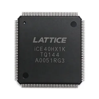
LFE2-6E-5TN144I - 6K LUT ECP2 FPGA | Lattice Semiconductor
MPN: LFE2-6E-5TN144I ✓ सक्रियLFE2-6E-5TN144I अवलोकन
An FPGA is a programmable digital-logic device in which lookup tables, registers, interconnect resources, and other blocks are configured after manufacture. ECP2 devices belong to Lattice Semiconductor's low-density FPGA family, placing them between fixed-function logic and larger programmable-logic devices. This makes the LFE2-6E-5TN144I useful for control logic, bus arbitration, interface bridging, signal conditioning, and embedded DSP when a microcontroller or discrete logic implementation would be less flexible.
Principal features include 6,000 logic cells, 6K LUTs, 90 I/O, one DSP block as identified in the product listing, and a 1.2 V operating core. The -5 suffix denotes the speed grade, while the final I identifies the industrial temperature option in Lattice Semiconductor's ECP2 ordering nomenclature. The TQFP-144 package provides 144 external pins and is compatible with conventional board-assembly and inspection processes.
The device supports parallel programmable-logic implementation and serial configuration workflows commonly used with ECP2 devices. Its approximately 6K LUT capacity is suitable for moderate control domains, not processor-heavy workloads or large video pipelines. Engineers should allocate flip-flops, interconnect, memory resources, DSP multipliers, and I/O standards concurrently because each placement can affect achievable timing and routing density.
Typical applications include industrial control, communications-interface bridging, test and measurement, embedded audio or motor-control signal processing, and compact embedded systems requiring field-updatable logic. The combination of 90 I/O and an embedded DSP block is particularly useful when a design needs parallel acquisition, digital filtering, protocol conversion, or deterministic control in one device.
PCB design should preserve the manufacturer's recommended power, decoupling, configuration, and clocking layout. Confirm the exact pin assignments, supported I/O standards, configuration interface, and timing constraints in the manufacturer datasheet before schematic capture. The -5 grade and industrial temperature suffix should also be checked against the system timing and environmental requirements.
This page consolidates the exact LFE2-6E-5TN144I attributes, same-package ECP2 alternatives, application guidance, and PCB design notes into one engineering-focused reference for FPGA selection, sourcing, and hardware implementation.
के लिए ड्रॉप-इन विकल्प LFE2-6E-5TN144I — समान पैकेज, पिन-टू-पिन संगत। PCB रीवर्क आवश्यक करने वाले भिन्न-पैकेज पार्ट्स शामिल नहीं हैं।
इस सीरीज़ के वेरिएंट
समान श्रृंखला के मॉडल जो ड्रॉप-इन संगत हैं LFE2-6E-5TN144I (समान फॉर्म फैक्टर और फुटप्रिंट) — इसमें भिन्न Package, Device Type, Speed Grade, Core Supply Voltage, Process Technology.
LFE2-6E-5TN144C
✅ ड्रॉप-इनकीमत के लिए संपर्क करें
डेटाशीट देखें →LFE2-6E-6TN144I
✅ ड्रॉप-इनकीमत के लिए संपर्क करें
डेटाशीट देखें →LFE2-6E-6TN144C
✅ ड्रॉप-इनकीमत के लिए संपर्क करें
डेटाशीट देखें →LFE2-6E-5T144I
✅ ड्रॉप-इनकीमत के लिए संपर्क करें
डेटाशीट देखें →LFE2-6SE-5TN144I
✅ ड्रॉप-इन📋 संदर्भ विकल्प (कैटलॉग में नहीं)
LFE2-6E-7TN144C
✅ ड्रॉप-इनकीमत के लिए संपर्क करें
डेटाशीट देखें →LFE2-6E-5TN144I Maximum Ratings और Electrical Characteristics
| Device Type | ECP2 field-programmable gate array |
| Logic Cells | 6,000 cells |
| Lookup Tables | 6K LUTs |
| User I/O | 90 I/O |
| DSP Blocks | 1 DSP block |
| Core Supply Voltage | 1.2 V |
| Speed Grade | -5 |
| Temperature Grade | Industrial |
| पैकेज | 144-pin TQFP |
| Process Technology | 90 nm |
| Device Family | LatticeECP2 |
| FPGA Type | Field-programmable gate array |
| माउंटिंग प्रकार | Surface mount |
LFE2-6E-5TN144I 144-pin tqfp पिन कॉन्फ़िगरेशन गाइड
LFE2-6E-5TN144I (144-pin tqfp पैकेज) के लिए पिन कॉन्फ़िगरेशन। इस डिजिटल IC में GPIO, संचार इंटरफ़ेस (UART, SPI, I2C) और पावर पिन शामिल हैं। वैकल्पिक पिन फ़ंक्शन और कॉन्फ़िगरेशन विकल्पों के लिए निर्माता डेटाशीट देखें। एम्बेडेड सिस्टम डिज़ाइन और PCB लेआउट के लिए आवश्यक।

इसके लिए कोई विस्तृत pinout data उपलब्ध नहीं: LFE2-6E-5TN144I.
देखें डेटाशीट पूर्ण पिन कॉन्फ़िगरेशन के लिए।
सामान्य अनुप्रयोग
LFE2-6E-5TN144I के लिए उपयुक्त है 6 अनुप्रयोगs: Industrial Control Logic, Communications Interface Bridging, Embedded DSP Signal Processing, Test and Measurement Equipment, Audio and Motor Signal Control, Embedded Security and Authentication.
Industrial Control Logic
The LFE2-6E-5TN144I fits industrial control tasks that combine parallel I/O, sequential logic, and deterministic signal handling in a compact 144-pin TQFP package. Its 6,000 logic cells and 6K LUTs provide enough resources for state machines, machine interlocks, counter and timer logic, and supervisory control, while 90 I/O can connect sensors, actuators, and industrial interfaces. The -5 speed grade and industrial temperature suffix align the ordering code with a demanding control environment. Compared with a microcontroller implementation, programmable logic can execute parallel interface conversion and timing functions deterministically without relying on real-time software scheduling.
अनुशंसित
Communications Interface Bridging
The LFE2-6E-5TN144I is suitable for protocol bridging, bus arbitration, data-format conversion, and parallel-to-serial interface logic where multiple independent channels must operate predictably. Its 90 I/O support parallel source and destination interfaces, while 6K LUTs can absorb framing logic, state management, and timing constraints. The embedded DSP block can also support filtering or modulation functions alongside the interface logic. Because an ECP2 design is reconfigurable, the same board platform can support several protocol combinations, provided the replacement candidate's -5, -6, or -7 speed grade and I or C temperature option satisfy the production requirements.
अनुशंसित
Embedded DSP Signal Processing
The LFE2-6E-5TN144I can implement DSP-assisted filtering, multiplication, waveform conditioning, and control functions in a single programmable device. Its one DSP block is useful when a design needs a dedicated arithmetic path, while the 6,000 logic cells handle configuration, state machines, counters, and surrounding interface control. The 1.2 V core and 90 I/O allow sampled data to remain within one FPGA implementation rather than moving between a processor and a separate accelerator. Engineering checks should include DSP timing closure, input and output register placement, and routing congestion around the arithmetic block.
अनुशंसित
Test and Measurement Equipment
The LFE2-6E-5TN144I fits programmable test and measurement front ends that coordinate acquisition, pattern generation, timing, and result handling. Its 90 I/O can connect sensors, stimulus sources, status signals, and synchronization lines, while 6K LUTs support counters, sequencing, and protocol-specific control. The field-programmable architecture allows measurement algorithms and stimulus sequences to be revised without changing the PCB, which is valuable for evolving automated test systems. Designers should preserve deterministic clocking, use registered I/O where timing demands it, and confirm that the selected speed and temperature grades meet the instrument's calibration environment.
अनुशंसित
Audio and Motor Signal Control
The LFE2-6E-5TN144I can combine digital filtering, waveform shaping, interpolation, or motor-control sequencing with real-time I/O handling. The embedded DSP block accelerates multiply-accumulate operations, while the programmable logic fabric manages sensor inputs, control outputs, fault flags, and timing. Its 90 I/O is useful for multichannel sampling, encoder interfaces, bridge-control signals, and supervisory status. The device is best suited to moderate algorithm sizes rather than large audio pipelines, and motor applications require careful grounding, isolation, and protection beyond the FPGA itself. Validate timing against the slowest required control loop and retain margin for the selected -5 grade.
अनुशंसित
Embedded Security and Authentication
The LFE2-6E-5TN144I is applicable to hardware-assisted authentication, key-decode, challenge-response, and protocol-security functions that benefit from parallelism and reconfiguration. Six thousand logic cells can implement multiple state machines or parallel comparisons, and the DSP block can accelerate arithmetic operations in selected algorithms. Ninety I/O provide connections to secure elements, sensors, communications channels, and status indicators. Because programmable devices are flexible, access control, protocol updates, and product variants can be consolidated into one platform. Review bitstream protection, configuration-port access, unused-pin behavior, and timing assumptions as part of the hardware security review.
अनुशंसित
अनुशंसित उत्पादों का सारांश
के लिए इंजीनियरिंग संदर्भ डेटा LFE2-6E-5TN144I — तुलना, डिज़ाइन मार्गदर्शन और अनुपालन जानकारी।
चयन गाइड
विकल्पों के साथ तुलना
| पैरामीटर | यह उत्पाद | LFE2-6E-5TN144C | LFE2-6E-6TN144I | LFE2-6E-6TN144C | LFE2-6E-5T144I | LFE2-6SE-5TN144I |
|---|---|---|---|---|---|---|
| Package | TQFP-144 | TQFP-144 | TQFP-144 | TQFP-144 | PQFP-144 / TQFP-144 | TQFP-144 |
| Brand | Lattice Semiconductor | Lattice Semiconductor | Lattice Semiconductor | Lattice Semiconductor | Lattice Semiconductor | Lattice Semiconductor |
| FPGA Family | LatticeECP2 | LatticeECP2 | LatticeECP2 | LatticeECP2 | ECP2 | ECP2 |
| Speed Grade | -5 | -5 | -6 | -6 | -5 | -5 |
| Temperature Suffix | I | C | I | C | I | I |
मुख्य विशेषताएँ
- Closest same-speed replacement (बनामLFE2-6E-5TN144C)
- Higher-rated timing option (बनामLFE2-6E-6TN144I)
- Broader commercial configuration (बनामLFE2-6E-7TN144C)
डिज़ाइन नोट्स
Assign the 1.2 V core and associated I/O supply domains according to the manufacturer power table. Place the required bulk and high-frequency decoupling capacitors at their designated supply pins, with the shortest possible return path to the ground or reference plane. Do not infer an I/O voltage merely from the 1.2 V core value; verify whether the selected TQFP-144 device uses a separate bank supply.
Follow the manufacturer's TQFP-144 footprint and pin-one orientation exactly. Preserve the orientation mark when defining the land pattern, and maintain the recommended pin-1 corner clearance. Because the alternatives use the same 144-pin package, verify that their configuration pins and supply assignments are electrically identical before treating the replacement as drop-in.
Do not substitute solely from the package drawing. The -5 and -6 parts differ in rated speed, while I and C suffixes identify different temperature options; the LFE2-6E and LFE2-6SE identifiers may also represent different device variants. Review the pin table, configuration scheme, timing class, temperature range, and bitstream compatibility before production substitution.
Use the manufacturer's clock-input and configuration guidance when assigning high-speed signals. Keep clock routing short and symmetric where possible, provide a clean clock source, and avoid routing sensitive inputs beside clocks or high-slew configuration nets. For external interfaces, confirm the supported I/O standard, drive strength, slew rate, and termination settings in the device documentation.
अनुपालन जानकारी
The target listing identifies a lead-free 144-pin package in related ECP2 comparison data, but no explicit RoHS, REACH, AEC-Q100, halogen-free, or conflict-minerals declaration for the exact target MPN was identified.