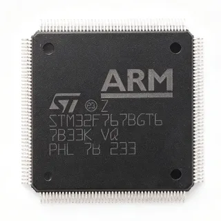
STM32H743BGT6 - 480MHz Cortex-M7 MCU 1MB Flash | STMicroelectronics
MPN: STM32H743BGT6 ✓ सक्रियSTM32H743BGT6 अवलोकन
An ARM Cortex-M7 microcontroller is a 32-bit RISC processor core with DSP extensions, a branch target cache, and tightly-coupled memory interfaces optimized for deterministic real-time control and signal processing. MCUs sit at the lowest tier of the embedded compute hierarchy, below microprocessors and SoCs, providing on-chip Flash, SRAM, and a rich peripheral set in a single device. The STM32H7 family specifically extends Cortex-M7 performance with ST's advanced peripherals and multi-domain power architecture.
Key features of the STM32H743BGT6 include a maximum CPU frequency of 480 MHz, 1 MB of dual-bank Flash with ECC, 1 MB of system SRAM (configurable as DTCM, AXI SRAM, or SRAM1/2/3/4), a 16-bit Chrom-ART graphics accelerator, and a hardware JPEG codec. Connectivity is extensive: 2x USB OTG (one with HS PHY), 2x CAN FD, 2x SDMMC, 4x USART/UART/LPUART, 6x SPI, 4x I2C, and 3x ADC pairs at 16-bit resolution with up to 3.6 MSPS. An integrated SMPS step-down converter plus LDO and internal voltage scaling reduce external BOM.
Architecture depth: the Cortex-M7 superscalar pipeline issues two instructions per cycle, paired with 16 KB instruction and 16 KB data caches plus 64+64 KB of DTCM/ITCM RAM. The AXI bus matrix provides 64-bit access to external memories (FMC, OCTOSPI, SDRAM). Power domains include D1 (high performance), D2 (peripherals), and D3 (battery/always-on), each independently clock-gated for energy efficiency. The device supports an operating range of 1.62 V to 3.6 V with separate I/O and core voltage rails.
Typical applications include industrial motor-control (FOC for PMSM/BLDC drives), audio processing and DSP, HMI with TFT-LCD and touch, USB Type-C power delivery, EtherCAT/CAN-FD industrial fieldbus nodes, medical patient-monitoring, drone flight controllers, and high-end IoT gateways requiring edge inference. The 1 MB Flash supports OTA-friendly dual-bank partitioning.
Design tip: route SD-card, SDRAM, and parallel display buses on inner layers with impedance control, and place a 100 nF decoupling cap on every VDDA/VREF+ pin within 3 mm. The integrated SMPS requires a 4.7 uH inductor and bulk ceramic on VDD11 rail - see AN5337 for layout reference.
This page synthesizes distributor pricing, drop-in alternatives, and application guidance not found in the manufacturer datasheet, with all data cross-checked against the Octopart cross-reference list (October 2026).
के लिए ड्रॉप-इन विकल्प STM32H743BGT6 — समान पैकेज, पिन-टू-पिन संगत। PCB रीवर्क आवश्यक करने वाले भिन्न-पैकेज पार्ट्स शामिल नहीं हैं।
इस सीरीज़ के वेरिएंट
समान श्रृंखला के मॉडल जो ड्रॉप-इन संगत हैं STM32H743BGT6 (समान फॉर्म फैक्टर और फुटप्रिंट) — इसमें भिन्न Package, ADC Resolution, Communication Interfaces, Core, Cryptographic Acceleration.
STM32H753BGT6
✅ ड्रॉप-इन ⚠️ विनिर्देश असत्यापितकीमत के लिए संपर्क करें
डेटाशीट देखें →STM32H742BGT6
✅ ड्रॉप-इन ⚠️ विनिर्देश असत्यापित📋 संदर्भ विकल्प (कैटलॉग में नहीं)
STM32H730BGT6
✅ ड्रॉप-इन ⚠️ विनिर्देश असत्यापित📋 संदर्भ विकल्प (कैटलॉग में नहीं)
STM32H743BGT6 Maximum Ratings और Electrical Characteristics
| Core Architecture | ARM Cortex-M7 32-bit |
| Maximum CPU Frequency | 480 MHz |
| FPU | Double-precision (DP-FPU) |
| DSP Extensions | Yes |
| L1 Cache | 16 KB I-cache + 16 KB D-cache |
| Program Flash | 1 MB (dual-bank with ECC) |
| System SRAM | 1 MB (DTCM + AXI + SRAM1-4) |
| Operating Voltage | 1.62 V to 3.6 V |
| पैकेज | 208-LQFP (28x28 mm) |
| माउंटिंग प्रकार | Surface Mount |
| ऑपरेटिंग तापमान | -40 C to +85 C |
| USB | 2x USB OTG (one HS PHY) |
| CAN | 2x CAN FD |
| ADC | 3x 16-bit, up to 3.6 MSPS |
| Graphics Accelerator | Chrom-ART (16-bit) |
| Hardware JPEG Codec | Yes |
| RoHS स्थिति | Compliant |
STM32H743BGT6 पिन कॉन्फ़िगरेशन
| पिन 1 | PE2 — GPIO PE2 / TRACECLK |
| पिन 2 | PE3 — GPIO PE3 / TRACED0 |
| पिन 3 | PE4 — GPIO PE4 / TRACED1 |
| पिन 4 | PE5 — GPIO PE5 / TRACED2 |
| पिन 5 | PE6 — GPIO PE6 / TRACED3 |
| पिन 6 | VBAT — Battery backup power input |
| पिन 7 | PC13 — GPIO PC13 / Tamper-RTC |
| पिन 8 | PC14 — GPIO PC14 / OSC32_IN |
| पिन 9 | PC15 — GPIO PC15 / OSC32_OUT |
| पिन 10 | VSS — Digital ground |
| पिन 11 | VDD — Digital power supply 1.62-3.6 V |
| पिन 12 | VREF+ — ADC positive voltage reference |
| पिन 13 | PA0 — GPIO PA0 / UART4_TX / TIM5_CH1 |
| पिन 14 | PA1 — GPIO PA1 / UART4_RX / TIM5_CH2 |
| पिन 15 | PA2 — GPIO PA2 / USART2_TX |
| पिन 16 | PA3 — GPIO PA3 / USART2_RX |
| पिन 17 | VSS — Digital ground |
| पिन 18 | VDD — Digital power supply 1.62-3.6 V |
| पिन 19 | PA4 — GPIO PA4 / SPI1_NSS / DAC1_OUT |
| पिन 20 | PA5 — GPIO PA5 / SPI1_SCK / DAC2_OUT |
सामान्य अनुप्रयोग
STM32H743BGT6 के लिए उपयुक्त है 6 अनुप्रयोगs: Industrial Motor Control (FOC for PMSM/BLDC), Audio Processing and DSP, HMI with TFT-LCD Display and Touch, USB Type-C Power Delivery Sink/Source, EtherCAT / CAN-FD Industrial Fieldbus Node, Medical Patient Monitoring.
Industrial Motor Control (FOC for PMSM/BLDC)
The STM32H743BGT6's 480 MHz Cortex-M7 with double-precision FPU and DSP extensions makes it well suited to field-oriented control of PMSM and BLDC motors. The two 16-bit ADCs at 3.6 MSPS handle current sampling for the FOC algorithm, while the high-resolution timer (HRTIM) drives the inverter at 32 kHz with sub-microsecond dead-time insertion. The 1 MB Flash stores the FOC firmware plus CANopen stack; the 1 MB SRAM holds the SV-PWM modulation table and speed-controller state. Placed on the same 208-pin LQFP footprint as the rest of the H7 family, it scales to dual-axis FOC without needing an external DSP.
अनुशंसित
Audio Processing and DSP
Audio applications benefit from the STM32H743BGT6's Cortex-M7 with DSP instructions and dedicated SAII peripheral. The 480 MHz clock executes multi-band compressors, parametric EQ, and FFT-based analysis in real time, while the SPDIF-Rx and SAI interfaces stream up to 192 kHz / 24-bit audio I/O. The 1 MB SRAM stores the audio delay-line buffers for room-correction algorithms. Two DMA controllers offload sample transfers, leaving CPU cycles for processing. The integrated SMPS provides clean power to the analog audio chain with a single 4.7 uH inductor and bulk ceramic.
अनुशंसित
HMI with TFT-LCD Display and Touch
Human-machine interface designs use the STM32H743BGT6's Chrom-ART graphics accelerator to drive WVGA or WQVGA TFT-LCD panels at 60 Hz. The 16-bit parallel RGB interface connects directly to a 4.3 inch or 5 inch display, while the LTDC peripheral overlays layers without CPU intervention. The hardware JPEG codec accelerates on-screen image decoding, and the SDMMC interface stores assets on a uSD card. The capacitive-touch controller is read via I2C. The 1 MB Flash stores the GUI binaries; the 1 MB SRAM holds the frame buffer and the LVGL widget tree for a responsive feel.
अनुशंसित
USB Type-C Power Delivery Sink/Source
The STM32H743BGT6 supports USB Type-C Power Delivery up to 100 W with its integrated USB OTG FS and HS PHYs plus 2x CAN-FD for sideband control. The 480 MHz Cortex-M7 runs the USB-PD 3.1 protocol stack with sufficient margin for a multi-port hub, and the 1 MB Flash holds both the PD stack and the application firmware. The 1 MB SRAM buffers the PD state machine and the upstream system messages. The OCTOSPI interface links to a QSPI flash for fast firmware updates, while the integrated SMPS provides the VBUS switching rails.
अनुशंसित
EtherCAT / CAN-FD Industrial Fieldbus Node
Industrial fieldbus designs use the STM32H743BGT6's 2x CAN-FD plus 2x USART (EtherCAT over SPI/Ethernet) to act as a slave node on a real-time industrial bus. The Cortex-M7 at 480 MHz supports EtherCAT cycle times down to 50 us, with EtherCAT/IP and PROFINET stacks running on top. The 32-bit FMC bus drives 32 MB of external SDRAM for protocol-stack scratch memory, and the 1 MB Flash stores the application and slave stack. The 208-pin LQFP exposes all three SPIs for additional communication channels.
अनुशंसित
Medical Patient Monitoring
Medical patient-monitoring designs use the STM32H743BGT6's 3x 16-bit ADC at 3.6 MSPS to capture ECG, SpO2, and respiration channels with oversampling for EN 60601-1-2 noise rejection. The Cortex-M7 at 480 MHz runs DSP-based QRS detection and FFT heart-rate-variability analysis in real time. The 1 MB SRAM stores the rolling waveform buffer; the 1 MB Flash holds the algorithm plus the BLE stack for tablet connectivity. The 1.62 V to 3.6 V supply range accommodates 2x AA battery cells with an LDO post-regulator. The Cortex-M7's deterministic interrupt latency keeps ECG sampling jitter under 1 us.
अनुशंसित
अनुशंसित उत्पादों का सारांश
के लिए इंजीनियरिंग संदर्भ डेटा STM32H743BGT6 — तुलना, डिज़ाइन मार्गदर्शन और अनुपालन जानकारी।
चयन गाइड
विकल्पों के साथ तुलना
| पैरामीटर | यह उत्पाद | STM32H753BGT6 | STM32H742BGT6 | STM32H730BGT6 |
|---|---|---|---|---|
| Brand | STMicroelectronics | STMicroelectronics | STMicroelectronics | STMicroelectronics |
| Package | 208-LQFP (28x28 mm) | 208-LQFP (28x28 mm) - same | 208-LQFP (28x28 mm) - same | 208-LQFP (28x28 mm) - same |
| Core | ARM Cortex-M7 | ARM Cortex-M7 | ARM Cortex-M7 | ARM Cortex-M7 |
| Max CPU Frequency | 480 MHz | 480 MHz | 480 MHz | 550 MHz |
| Flash Memory | 1 MB | 1 MB | 1 MB | 128 KB |
| SRAM | 1 MB | 1 MB | 1 MB | 564 KB |
| Hardware Crypto | No | Yes (AES-256, SHA, TRNG, PKA) | No | No |
| Operating Temperature | -40 C to +85 C | -40 C to +85 C | -40 C to +85 C | -40 C to +85 C |
मुख्य विशेषताएँ
- Add hardware crypto accelerators without PCB rework (बनामSTM32H753BGT6)
- Highest Flash and SRAM in the H730 family (बनामSTM32H730BGT6)
- Same 480 MHz, fewer peripherals (बनामSTM32H742BGT6)
डिज़ाइन नोट्स
The STM32H743BGT6's integrated SMPS step-down requires a 4.7 uH inductor on the VDD11 rail and 4.7 uF X5R bulk ceramic on VDD11_OUT. Per ST's application note AN5337, the SMPS efficiency is 75-85% across load. Place a 100 nF ceramic decoupling cap on every VDD pin within 3 mm. The SMPS supports DCDC Mode 0/1/2 selection via user-option bits; Mode 1 (default) balances efficiency and quiescent current best for typical industrial use.
The 208-pin LQFP uses 0.5 mm pitch. Route SDRAM and FMC signals on inner layers with controlled impedance (50 ohm single-ended) and a 4-layer stack-up with continuous ground plane. Length-match the SDRAM address and clock within 1 mm. The OCTOSPI and SDMMC bus also benefit from length matching. Place the external oscillator within 5 mm of OSC_IN/OSC_OUT with a guard ring.
The 208-pin LQFP has a thermal resistance (theta_JA) of approximately 30 C/W on a 4-layer JEDEC test board. At full 480 MHz operation with all peripherals active, the part dissipates around 1.5 W, leading to a 45 C junction rise above ambient. For high-temperature industrial use at +85 C ambient, the 1.5 W power leaves a 15 C margin to the 125 C Tj limit. Use thermal vias under the LQFP leads for additional dissipation if the design is enclosed.
Common pitfalls: (1) Failing to enable the SMPS by setting VOS0 bit in PWR_D3CR to '1' before high-performance operation. (2) Configuring OCTOSPI in single-SPI mode instead of OSPI mode for maximum throughput. (3) Over-specifying the external clock source - a 25 MHz crystal with 20 pF load is the canonical reference. (4) Forgetting to disable the internal bootloader nBOOT0 bit for production - leaves BOOT0 pin floating in the application firmware.
अनुपालन जानकारी
RoHS and REACH compliant per ST's product page. Not AEC-Q100 qualified; for automotive designs, see the STM32H743BGT6A (industrial temperature range) or consider the STM32H743VGT6 in the same family.