UCC21530DWKR vs UCC21530QDWKRQ1 Perbandingan
Perbandingan bersamaan detil UCC21530DWKR dari Texas Instruments dan UCC21530QDWKRQ1 dari Texas Instruments. Bandingkan spesifikasi penting, parameter listrik, pengemasan, status cycle, harga, dan ketersediaan untuk menentukan komponen terbaik untuk kebutuhan desain Anda.

Texas Instruments
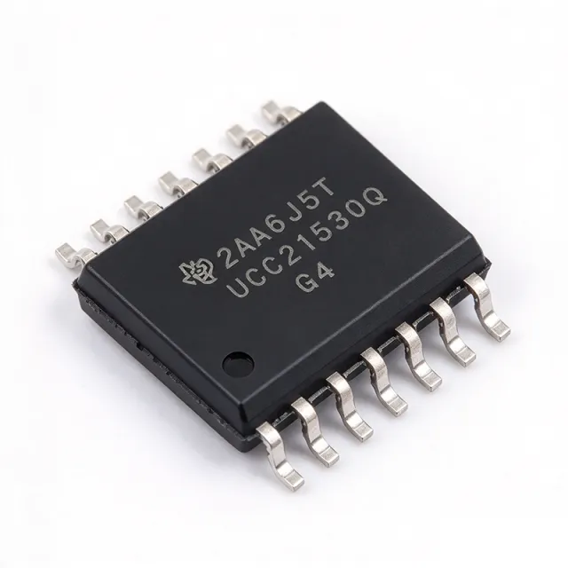
UCC21530QDWKRQ1 - 4A/6A 5.7kVrms Isolated Gate Driver | TI
UCC21530QDWKRQ1 ✓ AktifPerbandingan Spesifikasi
| Parameter Umum | UCC21530DWKR | UCC21530QDWKRQ1 |
|---|---|---|
| Merek | Texas Instruments | Texas Instruments |
| Kategori | Power MOSFET Drivers | Power MOSFET Drivers |
| Status Lingkungan Hidup | Aktif | Aktif |
| Status Stok | — | In Stock |
| Harga Unit (USD) | — | $1,07 |
| Driver Configuration | Half-Bridge (dual independent outputs) | — |
| Number of Channels | 2 | 2 (high-side / low-side) |
| Peak Source Current | 4 A | 4 A |
| Peak Sink Current | 6 A | 6 A |
| Isolation Voltage (RMS) | 5.7 kVRMS (reinforced, per UL 1577) | 5.7 kVRMS |
| Common-Mode Transient Immunity (CMTI) | >=125 V/ns (minimum) | 100 V/ns (minimum) |
| Channel-to-Channel Spacing | 3.3 mm | 3.3 mm (minimum) |
| Maximum Switching Frequency | 5 MHz | — |
| VDD Supply Range (logic side) | 3 V to 5.5 V | — |
| VDDA / VDDB Range (drive side) | 8 V to 18 V (up to 25 V per TI part details) | — |
| Propagation Delay | [DATA_NEEDED: propagation delay in ns] | — |
| Dead-Time Control | Programmable via DT pin resistor | — |
| Tombol Aktifkan | Yes (EN, active-high; pulls LOW to disable both outputs) | Yes (active-low) |
| Input Logic Compatibility | CMOS / TTL | — |
| Rentang Suhu Kerja | -40C to +125C | -40C to +125C |
| Paket | 14-SOIC (DWK) with 3.3 mm channel spacing | 14-pin SOIC (DWK wide-body) |
| Tipe Mounting | Surface Mount | Surface Mount |
| Approximate Datasheet Length | 47 pages (per third-party datasheet archive) | — |
| Status RoHS | Compliant | Compliant |
| Fungsi | — | Isolated dual-channel gate driver |
| Creepage / Clearance | — | 8.5 mm (DWK wide-body) |
| VDD/VDDA Supply Range | — | 18 V to 25 V (3 V to 18 V on logic side per datasheet) |
| Propagation Delay (Typical) | — | 33 ns |
| Maximum Operating Frequency | — | 5 MHz |
| Programmable Deadtime | — | Yes (DT pin) |
| Level MSL | — | 2 |
| AEC-Q100 Qualification | — | Qualified |
| Logic Input Compatibility | — | CMOS / TTL |