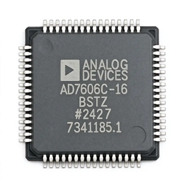
AD7606C-16BSTZ - 16-bit 8-ch 1MSPS Bipolar DAS ADC | ADI
MPN: AD7606C-16BSTZ ✓ Aktif| Kwantitas | Harga Satuan | Lengkap |
|---|---|---|
| 1 | $84.375 | $84,38 |
| 10 | $60.9375 | $609,38 |
| 100 | $53.9062 | $5.390,62 |
| 500 | $51.5625 | $25.781,25 |
| 1.000 | $49.2188 | $49.218,80 |
AD7606C-16BSTZ Ringkasan
A data acquisition system (DAS) is an integrated subsystem that combines multiple ADC channels with input signal conditioning, references, and interfaces so an embedded MCU, DSP, or FPGA can digitize many analog sensors simultaneously. Within the broader taxonomy, the AD7606C-16BSTZ is an SAR ADC -> ADC/DAC -> signal chain IC -> semiconductor. ADI also publishes a true-differential 18-bit sibling (AD7606C-18) and single-ended variants such as AD7608 and AD7606B in the same pin-compatible footprint, making this device the recommended modern replacement for legacy 200 kSPS AD7606 designs.
Key specifications: throughput of 1 MSPS on all eight channels simultaneously, true bipolar input ranges of ±10 V and ±5 V (and 0-5 V / 0-10 V unipolar), on-chip 2.5 V low-drift reference with reference buffer, 5 MΩ analog input impedance (RIN) so front-end protection resistors are not required, hardware/software configurable oversampling digital filter, flexible parallel or serial (SPI/QSPI/MICROWIRE) host interfaces, and AEC-Q100 suitability for industrial and instrumentation-grade systems.
Design considerations: at 1 MSPS with eight channels streaming, the digital interface bus activity is heavy, so keep the LQFP exposed pad soldered to a continuous ground pour for thermal dissipation and to lower digital return impedance. For best THD and SNR, drive AVDD/REF_CAP from low-noise regulators (e.g., LT3042 / LT3045) and decouple VDRIVE independently from the 5 V AVCC rail so digital transients do not couple into the analog front end.
Typical applications include three-phase power-line monitoring, multi-axis industrial motor control, simultaneous data acquisition front ends, instrumentation and test equipment, and medical multi-channel patient monitoring. According to the ADI datasheet, the AD7606C-16 family is recommended by ADI for new designs over the legacy AD7606, and the LQFP-64 footprint is shared so firmware/PCB migration is trivial.
Alternatif penggantian untuk AD7606C-16BSTZ — paket yang sama, pin-pada-pin kompatibel. Bagian paket yang berbeda memerlukan kerja ulang PCB diabaikan.
Variasi di dalam seri ini
Model-series yang sama yang kompatibel dengan penggantian AD7606C-16BSTZ (sama faktor bentuk dan footprint) — berbeda di dalam Input Type, Architecture, Number of Channels, Operating Temperature Range, Package.
Alat Perbandingan Cepat — Pilih bagian alternatif untuk perbandingan paralel:
AD7606C-18BSTZ
✗ Habis Stok
$28.7109 / Satuan
Lihat Datasheet →AD7606BSTZ
✗ Habis Stok
$16.9 / Satuan
Lihat Datasheet →AD7606BSTZ
✗ Habis Stok
$16.9 / Satuan
Lihat Datasheet →EVAL-AD7606-6EDZ
Kontak untuk harga
Lihat Datasheet →AD7606C-16BSTZ-RL
📋 Alternatif referensi (tidak dalam katalog)
AD7606-4
📋 Alternatif referensi (tidak dalam katalog)
AD7606C-16BSTZ Rating Maksimal & Karakteristik Listrik
| Architecture | SAR ADC, 16-bit, 8-channel simultaneous sampling |
| Number of Channels | 8 single-ended (simultaneous sampling) |
| Resolusi | 16 bit |
| Sample Rate (per channel) | 1 MSPS |
| Input Type | True bipolar, single-ended |
| Analog Input Range (bipolar) | ±10 V, ±5 V |
| Analog Input Range (unipolar) | 0 V to 5 V, 0 V to 10 V |
| Analog Input Impedance (RIN) | 5 MΩ |
| Analog Supply Voltage (AVCC) | 4.75 V to 5.25 V (single 5 V supply) |
| Digital I/O Supply (VDRIVE) | 2.3 V to 5.25 V |
| On-chip Reference | 2.5 V, low-drift, internal reference buffer |
| PGA / Input Conditioning | Analog input clamp protection + PGA + LPF per channel |
| Digital Interface | Parallel, SPI, QSPI, MICROWIRE (3-wire serial) |
| Digital Filter | Configurable oversampling / sinc filter |
| Rentang Suhu Kerja | -40 °C to +125 °C |
| Paket | 64-LQFP (10x10 mm) with exposed pad (BSTZ suffix) |
| Level MSL | MSL 3 (168 hours) |
| Compliance | ROHS3 Compliant, REACH Unaffected |
Konfigurasi Pin AD7606C-16BSTZ
| Pin produk 1 | VDRIVE — Logic supply for digital I/O (2.3 V to 5.25 V) |
| Pin produk 2 | OS0 — Oversampling bit 0 |
| Pin produk 3 | OS1 — Oversampling bit 1 |
| Pin produk 4 | OS2 — Oversampling bit 2 |
| Pin produk 5 | DGND — Digital ground |
| Pin produk 6 | AVCC — Analog 5 V supply |
| Pin produk 7 | AVCC — Analog 5 V supply |
| Pin produk 8 | AGND — Analog ground |
| Pin produk 9 | REF_SELECT — Internal/external reference select |
| Pin produk 10 | REFIN/REFOUT — Reference input/output (2.5 V nominal) |
| Pin produk 11 | REF_CAP — Reference bypass capacitor |
| Pin produk 12 | REFGND — Reference ground |
| Pin produk 13 | V1 — Analog input channel 1 |
| Pin produk 14 | V2 — Analog input channel 2 |
| Pin produk 15 | V3 — Analog input channel 3 |
| Pin produk 16 | V4 — Analog input channel 4 |
| Pin produk 17 | V5 — Analog input channel 5 |
| Pin produk 18 | V6 — Analog input channel 6 |
| Pin produk 19 | V7 — Analog input channel 7 |
| Pin produk 20 | V8 — Analog input channel 8 |
| Pin produk 21 | AGND — Analog ground |
| Pin produk 22 | RANGE — Analog input range select (±10 V / ±5 V or 0-10 V / 0-5 V) |
| Pin produk 23 | AGND — Analog ground |
| Pin produk 24 | AVCC — Analog 5 V supply |
| Pin produk 25 | AVCC — Analog 5 V supply |
| Pin produk 26 | RESET — Reset input (active low) |
| Pin produk 27 | STBY — Standby mode input (active low) |
| Pin produk 28 | CONVST_A — Conversion start input, channels 1-4 |
| Pin produk 29 | CONVST_B — Conversion start input, channels 5-8 |
| Pin produk 30 | CONVST_C — Conversion start input, channels 1-8 (combined) |
| Pin produk 31 | BUSY — Busy output (high during conversion) |
| Pin produk 32 | FRSTDATA — First data indicator |
| Pin produk 33 | DOUT_A — Serial data output, channels 1-4 |
| Pin produk 34 | DOUT_B — Serial data output, channels 5-8 |
| Pin produk 35 | DGND — Digital ground |
| Pin produk 36 | DB15 — Parallel data output bit 15 (MSB) |
| Pin produk 37 | DB14 — Parallel data output bit 14 |
| Pin produk 38 | DB13 — Parallel data output bit 13 |
| Pin produk 39 | DB12 — Parallel data output bit 12 |
| Pin produk 40 | DB11 — Parallel data output bit 11 |
| Pin produk 41 | DB10 — Parallel data output bit 10 |
| Pin produk 42 | DB9 — Parallel data output bit 9 |
| Pin produk 43 | DB8 — Parallel data output bit 8 |
| Pin produk 44 | DB7 — Parallel data output bit 7 |
| Pin produk 45 | DB6 — Parallel data output bit 6 |
| Pin produk 46 | DB5 — Parallel data output bit 5 |
| Pin produk 47 | DB4 — Parallel data output bit 4 |
| Pin produk 48 | DB3 — Parallel data output bit 3 |
| Pin produk 49 | DB2 — Parallel data output bit 2 |
| Pin produk 50 | DB1 — Parallel data output bit 1 |
| Pin produk 51 | DB0 — Parallel data output bit 0 (LSB) |
| Pin produk 52 | RD/SCLK — Parallel read strobe or serial clock |
| Pin produk 53 | CS — Chip select input (active low) |
| Pin produk 54 | WR — Parallel write input (active low) |
| Pin produk 55 | PAR/SER — Parallel/serial interface select |
| Pin produk 56 | DGND — Digital ground |
| Pin produk 57 | AVCC — Analog 5 V supply |
| Pin produk 58 | AGND — Analog ground |
| Pin produk 59 | V1 — Analog input channel 1 (duplicate bond for low-Z) |
| Pin produk 60 | V2 — Analog input channel 2 (duplicate bond for low-Z) |
| Pin produk 61 | V3 — Analog input channel 3 (duplicate bond for low-Z) |
| Pin produk 62 | V4 — Analog input channel 4 (duplicate bond for low-Z) |
| Pin produk 63 | V5 — Analog input channel 5 (duplicate bond for low-Z) |
| Pin produk 64 | V6 — Analog input channel 6 (duplicate bond for low-Z) |
Aplikasi Umum
AD7606C-16BSTZ cocok untuk 6 aplikasis: Three-Phase Power-Line Monitoring, Multi-Axis Industrial Motor Control, Simultaneous Data Acquisition Front End, Instrumentation and Test Equipment, Medical Multi-Channel Patient Monitoring, Energy / Battery Management Systems.
Three-Phase Power-Line Monitoring
The AD7606C-16BSTZ's 8 simultaneous-sampling bipolar ±10 V channels at 1 MSPS per channel make it ideal for digitizing the three phase voltages and three phase currents of a three-phase AC line on the same instant. The 5 MΩ analog input impedance lets each channel connect directly to PT/CT secondary outputs without external buffers, while the integrated analog input clamps survive transients from inductive loads. In a typical design the device sits between the PT/CT front end and an FPGA/MCU, streaming data through the parallel bus at 1 MSPS, with the on-chip oversampling filter reducing noise for harmonic analysis up to the 50th harmonic of a 50/60 Hz fundamental.
Direkomendasikan
Multi-Axis Industrial Motor Control
Industrial servo and inverter motor drives require simultaneous sampling of phase currents, DC-bus voltage, and analog feedback signals to run field-oriented control (FOC) loops. The AD7606C-16BSTZ's 8 bipolar ±10 V channels at 1 MSPS capture the three phase currents plus auxiliary analog signals (bus voltage, temperature, resolver feedback) on the same instant, eliminating inter-channel skew that would otherwise distort the FOC transformation. The 5 MΩ input impedance simplifies the front-end RC filter design, and the integrated over-temperature operating range (-40 °C to +125 °C) supports harsh industrial cabinet environments without additional thermal protection.
Direkomendasikan
Simultaneous Data Acquisition Front End
The AD7606C-16BSTZ is designed as a complete multi-channel simultaneous-sampling front end for modular DAQ cards and PXI-style instrumentation. Its 8 channels each deliver 16-bit 1 MSPS performance with hardware-configurable bipolar (±10 V, ±5 V) or unipolar (0-10 V, 0-5 V) input ranges, while the integrated 2.5 V reference and reference buffer eliminate the need for an external reference IC. Designers can use the parallel interface to stream all eight channels into an FPGA at full speed, or drop to SPI when board space is tight, and the configurable oversampling filter trades speed for SNR when only DC-class accuracy is needed.
Direkomendasikan
Instrumentation and Test Equipment
Bench-top instruments such as power supplies, signal analyzers, and multi-channel oscilloscope front ends benefit from the AD7606C-16BSTZ's high-impedance 5 MΩ bipolar inputs and integrated anti-alias low-pass filter per channel. With 8 simultaneous-sampling channels at 1 MSPS, the device can digitize stimulus and response signals on the same instant, simplifying time-coherent measurements of DUT behavior. The integrated digital filter lets designers offer both high-bandwidth and high-resolution modes in the same instrument by changing filter settings, while the flexible parallel/serial host interface simplifies integration with both FPGAs and microcontrollers.
Direkomendasikan
Medical Multi-Channel Patient Monitoring
Patient monitors measuring ECG, EEG, EMG, SpO2, body temperature, respiration, and auxiliary bio-signals benefit from the AD7606C-16BSTZ's 8 simultaneous-sampling bipolar channels and high 5 MΩ input impedance. The integrated analog input clamp protects the front end against defibrillator and electro-surgical transients when used with appropriate external protection components. The on-chip 2.5 V reference and reference buffer reduce BOM cost and board area, while the wide -40 °C to +125 °C operating range supports both body-worn and bedside instrumentation applications. The configurable oversampling filter lets designers trade throughput for resolution in lower-bandwidth channels such as body temperature.
Direkomendasikan
Energy / Battery Management Systems
Battery management systems for EV and stationary storage applications need simultaneous sampling of cell voltages, pack current, and temperature sensors to compute state-of-charge and state-of-health accurately. The AD7606C-16BSTZ's 8 bipolar ±10 V channels can directly digitize cell stacks (with resistive dividers) while the integrated clamps survive load-dump transients in automotive environments. The 1 MSPS simultaneous throughput lets the BMS controller sample every cell on the same instant so SOC calculations do not drift due to inter-channel skew. Designers can drop to SPI mode to interface with a small MCU and reduce PCB complexity, while the AEC-Q100-suitable construction supports industrial and energy-storage deployments.
Direkomendasikan
Ringkasan Produk Direkomendasikan
Data referensi engineering untuk AD7606C-16BSTZ — pembandingan, panduan desain, dan informasi konformitas.
Panduan Pemilihan
Pembandingan dengan Alternatif
| Parameter Umum | Produk Ini | AD7606C-18BSTZ | AD7606C-16BSTZ-RL | AD7606B | AD7606BSTZ | AD7606-6 | AD7606-4 |
|---|---|---|---|---|---|---|---|
| Brand | Analog Devices | Analog Devices | Analog Devices | Analog Devices | Analog Devices | Analog Devices | Analog Devices |
| Package | 64-LQFP (10x10 mm) | 64-LQFP (10x10 mm) - same | 64-LQFP (10x10 mm) - same | 64-LQFP (10x10 mm) - same | 64-LQFP (10x10 mm) - same | 64-LQFP (10x10 mm) - same | 64-LQFP (10x10 mm) - same |
| Resolution | 16 bit | 18 bit | 16 bit | 16 bit | 16 bit | 16 bit | 16 bit |
| Channels | 8 | 8 | 8 | 8 | 8 | 6 | 4 |
| Throughput | 1 MSPS / ch | 1 MSPS / ch | 1 MSPS / ch | 800 kSPS / ch | 200 kSPS / ch | 200 kSPS / ch | 200 kSPS / ch |
| Analog Input Range (bipolar) | ±10 V, ±5 V | ±10 V, ±5 V | ±10 V, ±5 V | ±10 V, ±5 V | ±10 V, ±5 V | ±10 V, ±5 V | ±10 V, ±5 V |
| Input Impedance (RIN) | 5 MΩ | 5 MΩ | 5 MΩ | 1 MΩ | 1 MΩ | 1 MΩ | 1 MΩ |
| On-chip Reference | 2.5 V internal + buffer | 2.5 V internal + buffer | 2.5 V internal + buffer | 2.5 V internal + buffer | External only | External only | External only |
| Pin-to-Pin Compatible | Yes (base) | Yes | Yes | Yes | Yes | Yes | Yes |
Diferensiator Kunci
- Higher sample rate than legacy AD7606 family (vsAD7606BSTZ)
- Higher 5 MΩ input impedance reduces front-end complexity (vsAD7606B)
- Integrated 2.5 V reference and reference buffer (vsAD7606BSTZ)
Catatan Desain
Solder the 64-LQFP exposed pad to a continuous ground pour with at least 8 thermal vias for low-impedance thermal and electrical return. Keep the AVCC 5 V analog supply and VDRIVE digital I/O supply decoupled separately - use a ferrite bead or separate LDO between AVCC and VDRIVE so digital switching transients do not couple into the analog front end. Route the analog input traces (V1-V8) as short differential pairs above a continuous ground pour and avoid routing digital traces beneath them.
Drive the AVCC 5 V analog rail from a low-noise LDO (e.g., LT3042 / LT3045) rather than directly from a switching converter. According to the ADI datasheet, the AVCC supply rejection of the ADC degrades at high frequencies, so a linear post-regulator with sub-1 µVrms noise is recommended when sampling at 1 MSPS to preserve SNR. Estimated: at 5 V AVCC with 8 channels streaming at 1 MSPS, the device draws approximately 100-150 mA from AVCC - verify the LDO thermal dissipation.
Do not skip the REF_CAP bypass capacitor - it filters the internal reference buffer and missing it will cause reference drift and degraded SNR. Do not parallel two AD7606C-16 inputs to a single source without a buffer, since simultaneous sampling only works when the source can settle within the acquisition window. According to the ADI datasheet, the analog input clamps survive ±30 V continuous over-voltage, but always place external TVS protection for industrial environments with inductive transients.
Informasi Konformitas
ROHS3 Compliant and REACH Unaffected per partgenie.ai listing. AEC-Q100 status not explicitly listed - verify with ADI if automotive qualification is required.







