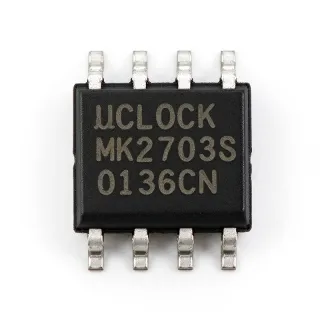
ICS663MI - PLL Clock Driver Building Block | Renesas | 8-SOIC
MPN: ICS663MI ✓ AktifICS663MI Ringkasan
A PLL building block is a timing IC used within a phase-locked-loop architecture. Its function is to support a feedback-controlled oscillator whose output frequency can be related to a reference frequency. Clock-generation and PLL-based frequency synthesis are part of the broader clock and timing hierarchy, which also includes clock buffers, clock drivers, dividers, oscillators, and frequency multipliers. These devices establish the timing reference used by processors, communications equipment, data converters, and digital control systems.
The defining physical characteristic of the ICS663MI is its 8-SOIC package with a stated width of 0.154 inch, or 3.90 mm. Surface mounting supports compact PCB construction and automated assembly. Renesas Electronics America Inc is identified as the manufacturer associated with the listed MPN, while legacy catalog records associate the part with Integrated Device Technology, Inc. The MI package suffix is treated as the manufacturer ordering code shown in the available listings.
The ICS663MI belongs to a timing-device category where exact operating limits must be established from the manufacturer datasheet before implementation. Input and output frequency ranges, supply voltage, operating temperature, phase noise, jitter, output configuration, and input-to-output ratio are not stated in the available product records. Those electrical parameters must be checked in the datasheet rather than inferred from the PLL building-block description. The package dimensions are known, but land-pattern and solder-reflow details also require manufacturer guidance.
Typical design roles for this device family include clock synthesis, reference distribution, communications timing, digital-system clock trees, and frequency conversion. In each case, the PLL is used to create or organize a stable timing relationship between a reference and an output clock. Whether the ICS663MI can support a particular channel rate, loop filter, output standard, or synchronization scheme depends on its detailed electrical characteristics and recommended application configuration.
Before layout, check the complete pin description and recommended decoupling network in the manufacturer datasheet. Keep the clock and feedback routing compact and controlled, and account for jitter and noise budget rather than treating the PLL solely as a frequency multiplier. PCB power and ground distribution, loop-filter component placement, and output-load compatibility are central to achieving predictable clock performance.
This product page combines the verified package and device-class information with practical selection guidance, comparison fields, sourcing questions, and design considerations. It separates confirmed facts from parameters that require datasheet confirmation, helping engineers determine whether the ICS663MI belongs in a clock-timing design before requesting a quote or beginning layout.
Alternatif penggantian untuk ICS663MI — paket yang sama, pin-pada-pin kompatibel. Bagian paket yang berbeda memerlukan kerja ulang PCB diabaikan.
Tidak ada alternatif pengganti yang tersedia untuk produk ini.
Permintaan AlternatifICS663MI Spesifikasi
| Device Type | IC PLL building block |
| Product Category | Clock and timing integrated circuit |
| Manufacturer | Renesas Electronics America Inc |
| Legacy Manufacturer | Integrated Device Technology, Inc. |
| Paket | 8-SOIC |
| Package Width | 3.90 mm (0.154 inch) |
| Jumlah Pin | 8 pins |
| Tipe Mounting | Surface mount |
ICS663MI 3.90 mm (0.154 inch) Diamant Konfigurasi Panduan
Konfigurasi pin untuk ICS663MI (3.90 mm (0.154 inch) pakai pakai). Penomoran pin, fungsi, dan diagram koneksi ditetapkan dalam datasheet produsen. Lihatnya untuk footprint dan pedoman perpindahan paruh.

Tidak ada data diatribut pin yang tersedia untuk ICS663MI.
Lihat ke: datasheet produk untuk konfigurasi pin penuh.
Aplikasi Umum
ICS663MI cocok untuk 6 aplikasis: Communications Clock Synthesis, Frequency Synthesis, Digital-System Clock Trees, Data-Converter Clocking, Industrial Control Timing, Test and Measurement Instrumentation.
Communications Clock Synthesis
The ICS663MI can be evaluated for communications clock synthesis because it is identified as an IC PLL building block and is implemented in an 8-SOIC package. In a communications system, this device could support a phase-locked timing relationship between a reference source and one or more derived clocks. However, suitability depends on the datasheet frequency range, output configuration, supply voltage, phase noise, and jitter. These electrical limits are not stated in the available product records and must be checked before selecting the device for a communications line rate, modulation scheme, or synchronization topology.
Frequency Synthesis
The ICS663MI is architecturally suited to frequency-synthesis work because its verified device function is a PLL building block. A designer could use this class of timing IC to establish an output frequency related to a stable reference through a feedback loop. The actual usable multiplication or division range, reference input frequency, output maximum, and tuning sensitivity must be confirmed from the manufacturer datasheet. Those parameters determine whether the ICS663MI can meet a specific synthesizer architecture without changing the loop-filter design or introducing excessive jitter.
Digital-System Clock Trees
A PLL building block can serve as the synthesis element within a digital-system clock tree, with downstream buffers providing fan-out to processors, memory, converters, and peripherals. The ICS663MI’s 8-SOIC package supports surface-mount assembly and can be considered where an eight-pin timing stage is appropriate. Designers must verify its output waveform, drive capability, supply level, and jitter against the complete clock tree. The ICS663MI should not be assumed to replace a dedicated fan-out buffer because synthesis and distribution have different noise, loading, and channel-count requirements.
Data-Converter Clocking
The ICS663MI may be considered for clocking data converters when the converter requires a derived, phase-locked sampling or modulation clock. The device’s verified PLL-building-block classification makes it relevant to that architecture, while the compact 8-SOIC package can simplify board planning. Suitability depends on required frequency, jitter, phase noise, edge quality, and output format. These specifications are not included in the available catalog records. Confirm them from the datasheet and include converter clock requirements when evaluating the complete jitter and noise budget.
Industrial Control Timing
Industrial control systems often need deterministic clock relationships across control, sensing, communication, and power-conversion subsystems. The ICS663MI’s PLL-building-block role can support such timing generation where a phase-locked reference is required. Its use in an industrial environment must be checked against the manufacturer’s operating-temperature and qualification information, neither of which is stated in the available listings. Also verify supply tolerance, clock-output levels, and jitter against the system timing budget before treating the part as suitable for factory-floor equipment.
Test and Measurement Instrumentation
The ICS663MI can be evaluated for phase-locked timing inside test and measurement instruments that require stable reference-derived clocks. The device could participate in a PLL-based frequency relationship or clock-generation path, but measurement accuracy depends on phase noise, jitter, spurs, and loop stability. Those parameters require direct review of the manufacturer datasheet. Because the confirmed package is 8-SOIC, board construction remains compatible with standard surface-mount assembly, while thermal and noise performance must be assessed for the intended instrument enclosure and ambient conditions.
Data referensi engineering untuk ICS663MI — pembandingan, panduan desain, dan informasi konformitas.
Panduan Pemilihan
Pembandingan dengan Alternatif
| Parameter Umum | Produk Ini |
|---|---|
| Brand | Renesas Electronics |
| Package | 8-SOIC |
| Package Width | 3.90 mm (0.154 inch) |
| Device Type | IC PLL building block |
| Product Category | Clock and timing integrated circuit |
Diferensiator Kunci
- Dedicated PLL building-block positioning (vsGeneric 8-SOIC clock buffer)
- Compact eight-pin implementation (vsLarger multi-output PLL)
- Clock synthesis and distribution remain separate functions (vsCombined synthesis-and-buffer device)
Catatan Desain
Follow the manufacturer’s recommended PLL layout for the ICS663MI, with special attention to the feedback divider, loop-filter components, reference input, and clock outputs. Keep feedback routing short and isolate it from noisy switching nodes. Place bypass and filter capacitors close to their associated pins, and use a continuous ground reference where the package and board construction permit. Because the available records do not identify the individual pin functions, the manufacturer pin table and reference layout should control track assignment.
Budget phase noise, jitter, spurs, and output loading as a single clock-quality requirement. Verify the ICS663MI’s specified output waveform and drive capability before connecting cable, high-speed digital, divider, or buffer loads. Keep output traces short, use controlled-impedance routing where relevant, and avoid stubs or test-point structures that create unnecessary reflections. If the PLL output feeds multiple destinations, place the distribution buffer near the source rather than using long point-to-point clock branches.
Do not select the ICS663MI solely because its eight-pin SOIC package matches an existing board. Confirm pin names, supply voltage, reference frequency, output frequency range, and loop configuration from the manufacturer datasheet. PLL parts can have similar packages while differing in output architecture, phase detector design, and division ratios. Also check decoupling requirements and operating-temperature limits. A package-level cross reference should be treated as the start of qualification rather than proof of drop-in compatibility.
Informasi Konformitas
Compliance declarations are not stated in the available product records and must be confirmed from the manufacturer documentation.