Renesas Electronics

ICS663MI - PLL Clock Driver Building Block | Renesas | 8-SOIC

部品番号: ICS663MI ✓ 生産中
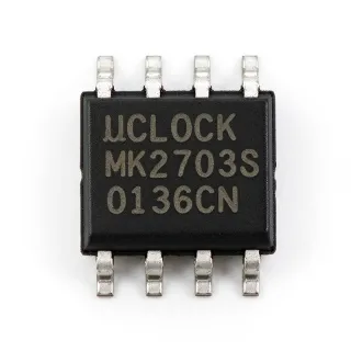
8-SOIC Package
MOQ: 1 |

ICS663MI 概要

Renesas ICS663MI is an integrated PLL building block packaged in an 8-pin SOIC, a surface-mount package measuring 3.90 mm wide. The component belongs to the clock and timing semiconductor family and is intended for clock-generation, clock-distribution, and frequency-synthesis systems. The verified product information identifies it as an IC PLL building block and lists the package as 8-SOIC.

A PLL building block is a timing IC used within a phase-locked-loop architecture. Its function is to support a feedback-controlled oscillator whose output frequency can be related to a reference frequency. Clock-generation and PLL-based frequency synthesis are part of the broader clock and timing hierarchy, which also includes clock buffers, clock drivers, dividers, oscillators, and frequency multipliers. These devices establish the timing reference used by processors, communications equipment, data converters, and digital control systems.

The defining physical characteristic of the ICS663MI is its 8-SOIC package with a stated width of 0.154 inch, or 3.90 mm. Surface mounting supports compact PCB construction and automated assembly. Renesas Electronics America Inc is identified as the manufacturer associated with the listed MPN, while legacy catalog records associate the part with Integrated Device Technology, Inc. The MI package suffix is treated as the manufacturer ordering code shown in the available listings.

The ICS663MI belongs to a timing-device category where exact operating limits must be established from the manufacturer datasheet before implementation. Input and output frequency ranges, supply voltage, operating temperature, phase noise, jitter, output configuration, and input-to-output ratio are not stated in the available product records. Those electrical parameters must be checked in the datasheet rather than inferred from the PLL building-block description. The package dimensions are known, but land-pattern and solder-reflow details also require manufacturer guidance.

Typical design roles for this device family include clock synthesis, reference distribution, communications timing, digital-system clock trees, and frequency conversion. In each case, the PLL is used to create or organize a stable timing relationship between a reference and an output clock. Whether the ICS663MI can support a particular channel rate, loop filter, output standard, or synchronization scheme depends on its detailed electrical characteristics and recommended application configuration.

Before layout, check the complete pin description and recommended decoupling network in the manufacturer datasheet. Keep the clock and feedback routing compact and controlled, and account for jitter and noise budget rather than treating the PLL solely as a frequency multiplier. PCB power and ground distribution, loop-filter component placement, and output-load compatibility are central to achieving predictable clock performance.

This product page combines the verified package and device-class information with practical selection guidance, comparison fields, sourcing questions, and design considerations. It separates confirmed facts from parameters that require datasheet confirmation, helping engineers determine whether the ICS663MI belongs in a clock-timing design before requesting a quote or beginning layout.

ドロップイン代替品: ICS663MI — 同一パッケージでピン互換。PCBの作り直しが必要な異なるパッケージの部品は除外されています。

この製品に利用可能なドロップイン代替品はありません。

代替品をリクエスト

ICS663MI 仕様

Device Type IC PLL building block
Product Category Clock and timing integrated circuit
Manufacturer Renesas Electronics America Inc
Legacy Manufacturer Integrated Device Technology, Inc.
パッケージ 8-SOIC
Package Width 3.90 mm (0.154 inch)
ピン数 8 pins
実装タイプ Surface mount

ICS663MI 3.90 mm (0.154 inch) ピン配置ガイド

ICS663MI (3.90 mm (0.154 inch) パッケージ) のピン配置。 ピン番号、機能、接続図はメーカーのデータシートで定義されています。正確なフットプリントとはんだ付けのガイドラインについては、データシートを参照してください。

ICS663MI の 3.90 mm (0.154 inch) パッケージピン配置図

詳細なピン配置データはありません: ICS663MI.

詳細は データシート をご参照ください。

主な用途

ICS663MI の用途: 6 件s: Communications Clock Synthesis, Frequency Synthesis, Digital-System Clock Trees, Data-Converter Clocking, Industrial Control Timing, Test and Measurement Instrumentation.

🌐

Communications Clock Synthesis

The ICS663MI can be evaluated for communications clock synthesis because it is identified as an IC PLL building block and is implemented in an 8-SOIC package. In a communications system, this device could support a phase-locked timing relationship between a reference source and one or more derived clocks. However, suitability depends on the datasheet frequency range, output configuration, supply voltage, phase noise, and jitter. These electrical limits are not stated in the available product records and must be checked before selecting the device for a communications line rate, modulation scheme, or synchronization topology.

🔧

Frequency Synthesis

The ICS663MI is architecturally suited to frequency-synthesis work because its verified device function is a PLL building block. A designer could use this class of timing IC to establish an output frequency related to a stable reference through a feedback loop. The actual usable multiplication or division range, reference input frequency, output maximum, and tuning sensitivity must be confirmed from the manufacturer datasheet. Those parameters determine whether the ICS663MI can meet a specific synthesizer architecture without changing the loop-filter design or introducing excessive jitter.

🖥️

Digital-System Clock Trees

A PLL building block can serve as the synthesis element within a digital-system clock tree, with downstream buffers providing fan-out to processors, memory, converters, and peripherals. The ICS663MI’s 8-SOIC package supports surface-mount assembly and can be considered where an eight-pin timing stage is appropriate. Designers must verify its output waveform, drive capability, supply level, and jitter against the complete clock tree. The ICS663MI should not be assumed to replace a dedicated fan-out buffer because synthesis and distribution have different noise, loading, and channel-count requirements.

📺

Data-Converter Clocking

The ICS663MI may be considered for clocking data converters when the converter requires a derived, phase-locked sampling or modulation clock. The device’s verified PLL-building-block classification makes it relevant to that architecture, while the compact 8-SOIC package can simplify board planning. Suitability depends on required frequency, jitter, phase noise, edge quality, and output format. These specifications are not included in the available catalog records. Confirm them from the datasheet and include converter clock requirements when evaluating the complete jitter and noise budget.

🏭

Industrial Control Timing

Industrial control systems often need deterministic clock relationships across control, sensing, communication, and power-conversion subsystems. The ICS663MI’s PLL-building-block role can support such timing generation where a phase-locked reference is required. Its use in an industrial environment must be checked against the manufacturer’s operating-temperature and qualification information, neither of which is stated in the available listings. Also verify supply tolerance, clock-output levels, and jitter against the system timing budget before treating the part as suitable for factory-floor equipment.

🔧

Test and Measurement Instrumentation

The ICS663MI can be evaluated for phase-locked timing inside test and measurement instruments that require stable reference-derived clocks. The device could participate in a PLL-based frequency relationship or clock-generation path, but measurement accuracy depends on phase noise, jitter, spurs, and loop stability. Those parameters require direct review of the manufacturer datasheet. Because the confirmed package is 8-SOIC, board construction remains compatible with standard surface-mount assembly, while thermal and noise performance must be assessed for the intended instrument enclosure and ambient conditions.

What is the ICS663MI?
The ICS663MI is an IC PLL building block from Renesas Electronics America Inc, packaged in an 8-SOIC. It is a clock-and-timing semiconductor intended to participate in phase-locked-loop designs that generate, divide, distribute, or relate clock signals. According to the ICS663MI manufacturer datasheet, its function is identified as a PLL building block; detailed electrical limits should be confirmed from the datasheet before final circuit design.
What package does the ICS663MI use?
The ICS663MI uses an 8-SOIC surface-mount package with a listed width of 0.154 inch, or 3.90 mm. The package designation and eight-pin construction identify the physical land pattern required for PCB compatibility. Use the manufacturer pin-description table and package drawing when assigning signals, and verify soldering and land-pattern details against the datasheet rather than relying only on the package name.
Where can I download the ICS663MI datasheet PDF?
The ICS663MI datasheet PDF can be accessed through the linked manufacturer-datasheet record on this page. The document is titled ICS663MI Datasheet and is indexed under Integrated Circuit Systems. Use it to confirm the complete pinout, electrical limits, recommended application circuit, loop-filter guidance, and package drawing before releasing a PCB layout or production design.
Where can I find the ICS663MI pinout?
The ICS663MI pinout is defined by the manufacturer datasheet and corresponds to its eight-pin SOIC package. Because the individual terminal names are not included in the available product records, use the datasheet pin-description table for authoritative numbering and signal assignments. Keep the footprint, pin-one orientation, and exposed versus unconnected terminals consistent with that table during PCB layout.
What are the key specifications of ICS663MI that engineers should know?
The confirmed ICS663MI specifications are its function as an IC PLL building block, its 8-SOIC package, and its 3.90 mm package width. Input and output frequency limits, supply voltage, phase noise, jitter, temperature range, and loop characteristics are not stated in the product records and must be obtained from the manufacturer datasheet. This distinction prevents unsupported assumptions during architecture selection.
Is the ICS663MI suitable for communications clock generation?
The ICS663MI may be suitable for communications clock-generation designs when its datasheet limits satisfy the required reference and output frequencies. As a PLL building block, it is architecturally relevant to phase-locked timing systems, but the available records do not state frequency range, jitter, phase noise, or output-drive capability. Verify those parameters and the recommended loop-filter configuration before committing the part.
What is the difference between a PLL building block and a clock buffer?
A PLL building block supports a feedback-controlled oscillator used to establish a phase-locked relationship between signals, while a clock buffer reproduces and distributes an existing clock with low added distortion. The ICS663MI is identified specifically as a PLL building block, so it belongs to the synthesis side of a clock-and-timing system. A separate buffer may still be needed to fan out its output.
Can the ICS663MI be used as a drop-in replacement in an existing PCB?
The ICS663MI should not be treated as a drop-in replacement without verification. Its confirmed package is 8-SOIC, but same-package construction alone does not establish pin compatibility, electrical equivalence, or equivalent PLL behavior. A valid replacement must match the existing footprint and pin functions, then satisfy frequency, voltage, jitter, noise, and application requirements. No verified drop-in substitute is identified on this page.
What is the best drop-in replacement for ICS663MI?
No verified best drop-in replacement for the ICS663MI is established by the available cross-reference results. The search results provide general component-matching tools but do not identify a specific substitute with confirmed pin compatibility and matching electrical characteristics. Use the manufacturer cross-reference process and compare the complete pin list, frequency limits, supply voltage, phase noise, jitter, and recommended application circuit before approving any replacement.
What can replace the ICS663MI?
A component can replace the ICS663MI only after its eight-pin SOIC footprint, pin functions, supply requirements, frequency range, and timing performance are verified. No specific alternative MPN is established as a drop-in replacement in the available records, and similarly packaged clock ICs may have different loop architectures or output configurations. Treat any proposed substitute as a new engineering qualification rather than an automatic substitution.
ICS663MI vs a generic PLL multiplier: which is better for a clock tree?
The ICS663MI is better when a design specifically requires a documented PLL building block in an 8-SOIC package and the timing limits match the application. A generic PLL multiplier may be preferable when it offers a higher multiplication factor, lower jitter, differential outputs, or a newer clock architecture. Since the generic device is not an identified verified alternative, compare the required clock-tree outputs and quantitative timing specifications directly.
When should I choose ICS663MI over another clock-timing IC?
Choose the ICS663MI when its 8-SOIC PLL-building-block architecture, documented operating limits, and application configuration satisfy the design requirement. Prefer another clock IC when it offers required features such as higher output frequency, lower jitter, differential clock outputs, integrated dividers, or better power performance. A datasheet-level comparison is essential because the available product records do not establish comparable electrical ratings.
What design considerations apply to a PCB using ICS663MI?
A PCB using the ICS663MI should follow the manufacturer’s recommended power, ground, feedback, and output-routing configuration. Keep PLL feedback and clock traces short, place loop-filter components according to the reference design, and maintain a continuous ground reference under the device where the package drawing permits it. Account for output loading and jitter budget when adding downstream clock-buffer stages.
How should power and grounding be handled around the ICS663MI?
Power and grounding around the ICS663MI should follow the decoupling and layout guidance in the manufacturer datasheet. Because the device is a PLL building block, reference noise and feedback instability can degrade phase noise or cause clock jitter. Use the specified bypass capacitors, provide a low-impedance return path, and avoid routing noisy switching-current paths beneath or immediately beside sensitive clock and feedback nodes.
Where can I buy the ICS663MI online?
Use the Request a Quote form on this page to ask about ICS663MI availability, current commercial terms, and lead time. The form is the appropriate route for obtaining an exact quotation because market price and inventory can change with quantity, date, and delivery requirements. Provide the MPN, required quantity, and target shipment region when submitting the request.
What is the price and lead time for the ICS663MI?
Current price and lead time for the ICS663MI should be requested through the Request a Quote form on this page. The available listings do not provide a qualifying quantity-break price table for the exact MPN, so no static price or lead-time figure is asserted here. Include required quantity, packaging preference, ship-to country, and target delivery date in the request for a meaningful response.
Is the ICS663MI in stock?
Inventory status for the ICS663MI should be confirmed through the Request a Quote form on this page. Some distributor records display historical or changing stock quantities, but those figures are not a reliable promise of current availability. State the required quantity and delivery target so the quotation can reflect the exact order and any sourcing or fulfillment constraints.

エンジニアリング参考データ: ICS663MI — 比較、設計ガイダンス、コンプライアンス情報。

選定ガイド

Choose the ICS663MI when an eight-pin SOIC PLL building block matches the mechanical design and the manufacturer datasheet confirms that its frequency, supply, noise, jitter, and temperature limits satisfy the application. It is most relevant to communications timing, frequency-synthesis, digital clock-tree, data-converter, industrial-control, and test-instrument designs that require a phase-locked timing relationship. Select another clock-and-timing IC when the design needs higher maximum frequencies, lower jitter, lower phase noise, differential outputs, more output channels, integrated dividers, or a documented fan-out buffer. No verified drop-in replacement is established, so an existing PCB should not be respooled solely because a candidate has an eight-pin SOIC package. Validate pin functions, electrical limits, loop-filter configuration, output compatibility, and lifecycle status before approving a substitute.

代替品との比較

パラメータ この製品
Brand Renesas Electronics
Package 8-SOIC
Package Width 3.90 mm (0.154 inch)
Device Type IC PLL building block
Product Category Clock and timing integrated circuit

主な差別化要因

  • Dedicated PLL building-block positioning (vs Generic 8-SOIC clock buffer)
  • Compact eight-pin implementation (vs Larger multi-output PLL)
  • Clock synthesis and distribution remain separate functions (vs Combined synthesis-and-buffer device)

設計ノート

Follow the manufacturer’s recommended PLL layout for the ICS663MI, with special attention to the feedback divider, loop-filter components, reference input, and clock outputs. Keep feedback routing short and isolate it from noisy switching nodes. Place bypass and filter capacitors close to their associated pins, and use a continuous ground reference where the package and board construction permit. Because the available records do not identify the individual pin functions, the manufacturer pin table and reference layout should control track assignment.

Budget phase noise, jitter, spurs, and output loading as a single clock-quality requirement. Verify the ICS663MI’s specified output waveform and drive capability before connecting cable, high-speed digital, divider, or buffer loads. Keep output traces short, use controlled-impedance routing where relevant, and avoid stubs or test-point structures that create unnecessary reflections. If the PLL output feeds multiple destinations, place the distribution buffer near the source rather than using long point-to-point clock branches.

Do not select the ICS663MI solely because its eight-pin SOIC package matches an existing board. Confirm pin names, supply voltage, reference frequency, output frequency range, and loop configuration from the manufacturer datasheet. PLL parts can have similar packages while differing in output architecture, phase detector design, and division ratios. Also check decoupling requirements and operating-temperature limits. A package-level cross reference should be treated as the start of qualification rather than proof of drop-in compatibility.

コンプライアンス情報

RoHS
Unknown
REACH
Unknown
AEC-Q100
Unknown
鉛フリー
Unknown
ハロゲンフリー
Unknown
紛争鉱物
Unknown

Compliance declarations are not stated in the available product records and must be confirmed from the manufacturer documentation.
関連検索

ICS663MI datasheet ICS663MI pinout ICS663MI datasheet pdf ICS663MI equivalent ICS663MI replacement ICS663MI cross reference ICS663MI 8-SOIC ICS663MI clock generator ICS663MI price ICS663MI stock Renesas ICS663MI ICS663MI footprint

関連部品&用語

Renesas Electronics Renesas Electronics America Inc Integrated Device Technology ICS663MI PLL building block phase-locked loop clock generator clock driver clock buffer frequency synthesizer clock and timing IC integrated circuit semiconductor 8-SOIC SOIC package family surface mount SMD phase noise output jitter loop filter reference clock communications clock synthesis data-converter clocking industrial control timing
クイック見積RFQ
詳細をすべてご記入ください — 営業チームが24時間以内にご返信いたします
部品番号 メーカー パッケージ QTY 目標価格 小計
✓
見積を送信しました!

24時間以内にメールでご返信いたします

1
RFQ送信済み
2
見積受領
3
注文済み
4
お支払い
5
発送済み
6
配達済み
RFQの詳細を表示