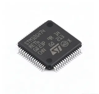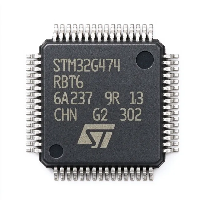
STM32G474RBT6 - 170MHz Cortex-M4F MCU 128KB LQFP-64 | STMicroelectronics
MPN: STM32G474RBT6 ✓ AktifSTM32G474RBT6 Ringkasan
An Arm Cortex-M4 microcontroller is a 32-bit RISC core with hardware floating-point and DSP extensions, intended for deterministic real-time signal processing. Within ST's portfolio it sits in the mainstream performance tier above Cortex-M0+ designs but below Cortex-M7 parts, delivering high analog integration combined with DSP throughput. The STM32G4 line is positioned for power conversion, motor control, digital power, lighting, and wireless charging.
Key features include 170 MHz CPU, 128 KB dual-bank Flash, 32 KB SRAM (with 16 KB SRAM with parity + 16 KB SRAM with ECC option depending on variant), 4 KB backup SRAM, hardware math accelerator for CORDIC + FIR/IIR filters, low-power run, sleep, stop, standby, and shutdown modes, and a working temperature range of -40 C to +85 C (grade 6 suffix). The 64-pin LQFP also exposes CAN FD, FDCAN, USB Type-C Power Delivery, and three SPI/three I2C/three USART plus UART/LIN interfaces.
The device implements ST's ART Accelerator (zero-wait-state Flash execution), a prefetch buffer, MPU, and JTAG/SWD debug with ETM trace. Internal regulators accept 1.71 V to 3.6 V supply and provide separate core and analog rails, allowing PVD programmable voltage detection down to 1.8 V with a brownout reset.
Typical applications include field-oriented motor control (FOC) for BLDC/PMSM, digital switched-mode power supplies (PFC + LLC), solar micro-inverters, LED lighting drivers, wireless charging Tx/Rx pumps, and industrial SMPS. Compared to discrete analog designs the integrated op-amps and comparators reduce BOM cost and accelerate current-loop bandwidth by eliminating external amplifiers in the shunt-sensing path.
When designing with the STM32G474RBT6, ensure VDDA is decoupled with a 100 nF + 1 uF pair close to the pin and add a ferrite bead between VDD and VDDA to keep digital switching noise out of the ADC reference. Select an external LDO or internal SMPS step-down configuration per the application note; for 500 mA peak loops fit at least 4-layer PCB layout with 1 oz copper.
This page synthesizes distributor stock data (DigiKey, Mouser, LCSC, Wolfchip), 5 pin-compatible drop-in alternatives with parametric proximity scores, and PCB layout notes that are not duplicated in the manufacturer datasheet.
Alternatif penggantian untuk STM32G474RBT6 — paket yang sama, pin-pada-pin kompatibel. Bagian paket yang berbeda memerlukan kerja ulang PCB diabaikan.
Variasi di dalam seri ini
Model-series yang sama yang kompatibel dengan penggantian STM32G474RBT6 (sama faktor bentuk dan footprint) — berbeda di dalam Flash Memory, Package, Comparators, Core, Operational Amplifiers.
STM32G474RBT3
Kontak untuk harga
Lihat Datasheet →STM32G474CET6
Kontak untuk harga
Lihat Datasheet →STM32G474CBT3
Kontak untuk harga
Lihat Datasheet →STM32G473QCT6
Kontak untuk harga
Lihat Datasheet →STM32G431CBU6
Kontak untuk harga
Lihat Datasheet →GD32G553RET7
📋 Alternatif referensi (tidak dalam katalog)
STM32G474RBT6 Rating Maksimal & Karakteristik Listrik
| Core | Arm Cortex-M4F with FPU + DSP |
| Maximum CPU Frequency | 170 MHz |
| DMIPS | 213 |
| Flash Memory | 128 KB (dual-bank) |
| SRAM | 32 KB (data) |
| Backup SRAM | 4 KB |
| Supply Voltage (VDD/VDDA) | 1.71 V to 3.6 V |
| Paket | 64-pin LQFP (10x10 mm) |
| Suhu Kerja | -40 C to +85 C (grade 6) |
| GPIO Count | 52 (on 64-pin package) |
| 12-bit ADC | 5x ADC, up to 4 MSPS |
| 12-bit DAC | 4x DAC (3 buffered + 1 unbuffered) |
| Comparators | 7x ultra-high-speed |
| Operational Amplifiers | 4x on-chip op-amps |
| Math Accelerator | CORDIC + FMAC + filter engine |
| Advanced timers | 2x 16-bit (10 ch each) |
| General-purpose timers | 5x 16-bit + 2x 32-bit |
| CAN FD | 1x FDCAN |
| USB Type-C / USB PD | Yes (USB 2.0 FS + UCPD) |
| Status RoHS | Compliant |
Konfigurasi Pin STM32G474RBT6
| Pin produk 1 | PC13 — GPIO/Tamper-RTC/Event-out |
| Pin produk 2 | PC14/OSC32_IN — GPIO/LSE 32.768 kHz oscillator input |
| Pin produk 3 | PC15/OSC32_OUT — GPIO/LSE 32.768 kHz oscillator output |
| Pin produk 4 | VSS_1 — Ground reference 1 |
| Pin produk 5 | VDD_1 — Digital supply 1 (1.71-3.6 V) |
| Pin produk 6 | PH0/OSC_IN — HSE oscillator input / GPIO |
| Pin produk 7 | PH1/OSC_OUT — HSE oscillator output / GPIO |
| Pin produk 8 | NRST — Reset (active low) |
| Pin produk 9 | PA0 — GPIO/ADC1_IN5/TIM2_CH1/OPAMP1_VINP |
| Pin produk 10 | PA1 — GPIO/ADC1_IN6/TIM2_CH2/OPAMP1_VINM/OPAMP1_VOUT |
| Pin produk 11 | PA2 — GPIO/USART2_TX/ADC1_IN7/OPAMP1_VINP |
| Pin produk 12 | PA3 — GPIO/USART2_RX/ADC1_IN8/OPAMP1_VINM |
| Pin produk 13 | PA4 — GPIO/ADC2_IN9/DAC1_OUT1/OPAMP2_VINP |
| Pin produk 14 | PA5 — GPIO/ADC2_IN10/DAC1_OUT2/OPAMP2_VINM |
| Pin produk 15 | PA6 — GPIO/ADC2_IN11/DAC2_OUT1/OPAMP2_VOUT |
| Pin produk 16 | PA7 — GPIO/ADC2_IN12/DAC2_OUT2/OPAMP2_VINP |
| Pin produk 17 | PA8 — GPIO/TIM1_CH1/HRTIM_CHA1 |
| Pin produk 18 | PA9 — GPIO/TIM1_CH2/USART1_TX |
| Pin produk 19 | PA10 — GPIO/TIM1_CH3/USART1_RX |
| Pin produk 20 | PA11 — GPIO/USB_DM/CAN1_RX/HRTIM_CHC2 |
| Pin produk 21 | PA12 — GPIO/USB_DP/CAN1_TX/HRTIM_CHC3 |
| Pin produk 22 | PA13 — GPIO/SWDIO |
| Pin produk 23 | VSS_2 — Ground reference 2 |
| Pin produk 24 | VDD_2 — Digital supply 2 |
| Pin produk 25 | PA14 — GPIO/SWCLK |
| Pin produk 26 | PA15 — GPIO/TIM2_CH1/SPI1_NSS |
| Pin produk 27 | PB0 — GPIO/ADC1_IN11/OPAMP3_VINP/TIM3_CH3 |
| Pin produk 28 | PB1 — GPIO/ADC1_IN12/OPAMP3_VINM/HRTIM_SCOUT |
| Pin produk 29 | PB2 — GPIO/BOOT0 (alternate) |
| Pin produk 30 | PB3 — GPIO/SPI1_SCK/TIM2_CH2 |
| Pin produk 31 | PB4 — GPIO/SPI1_MISO/TIM3_CH1 |
| Pin produk 32 | PB5 — GPIO/SPI1_MOSI/TIM3_CH2 |
| Pin produk 33 | PB6 — GPIO/USART1_TX/I2C1_SCL |
| Pin produk 34 | PB7 — GPIO/USART1_RX/I2C1_SDA |
| Pin produk 35 | PB8 — GPIO/I2C1_SCL/CAN1_RX |
| Pin produk 36 | PB9 — GPIO/I2C1_SDA/CAN1_TX |
| Pin produk 37 | PB10 — GPIO/USART3_TX/SPI2_SCK |
| Pin produk 38 | PB11 — GPIO/USART3_RX/SPI2_MISO |
| Pin produk 39 | PB12 — GPIO/SPI2_MOSI/TIM1_BKIN |
| Pin produk 40 | PB13 — GPIO/SPI2_SCK/TIM1_CH1N |
| Pin produk 41 | PB14 — GPIO/SPI2_MISO/TIM1_CH2N |
| Pin produk 42 | PB15 — GPIO/SPI2_MOSI/TIM1_CH3N |
| Pin produk 43 | PC0 — GPIO/ADC1_IN6/OPAMP3_VOUT/COMP1_INM |
| Pin produk 44 | PC1 — GPIO/ADC2_IN7/OPAMP1_VINP |
| Pin produk 45 | PC2 — GPIO/ADC3_IN8/OPAMP1_VINM |
| Pin produk 46 | PC3 — GPIO/ADC4_IN9/OPAMP1_VINP |
| Pin produk 47 | VSSA — Analog ground |
| Pin produk 48 | VDDA — Analog supply |
| Pin produk 49 | PC4 — GPIO/ADC2_IN14/COMP3_INP/USART1_TX |
| Pin produk 50 | PC5 — GPIO/ADC2_IN15/COMP3_INM/USART1_RX |
| Pin produk 51 | PC6 — GPIO/TIM3_CH1/I2C2_SCL |
| Pin produk 52 | PC7 — GPIO/TIM3_CH2/I2C2_SDA |
| Pin produk 53 | PC8 — GPIO/TIM3_CH3 |
| Pin produk 54 | PC9 — GPIO/TIM3_CH4 |
| Pin produk 55 | PA0/U5V_EN — GPIO/U5V enable |
| Pin produk 56 | PA1/VBUS — GPIO/VBUS sensing (UCPD) |
| Pin produk 57 | PC10 — GPIO/UART4_TX/SPI3_SCK |
| Pin produk 58 | PC11 — GPIO/UART4_RX/SPI3_MISO |
| Pin produk 59 | PC12 — GPIO/UART5_TX/SPI3_MOSI |
| Pin produk 60 | PD0 — GPIO/SPI4_NSS/TIM4_CH1 |
| Pin produk 61 | PD1 — GPIO/SPI4_SCK/TIM4_CH2 |
| Pin produk 62 | PD2 — GPIO/UART5_RX/TIM3_ETR |
| Pin produk 63 | VSS_3 — Ground reference 3 |
| Pin produk 64 | VDD_3 — Digital supply 3 |
Aplikasi Umum
STM32G474RBT6 cocok untuk 7 aplikasis: Field-Oriented Control (FOC) for BLDC / PMSM Motors, Digital Switched-Mode Power Supply (PFC + LLC), Wireless Charging Transmitter / Receiver, Industrial Servo Drives / Robotics, Solar Micro-Inverter / Energy Harvesting, Digital LED Lighting Drivers, E-Bike / E-Scooter Traction Controller.
Field-Oriented Control (FOC) for BLDC / PMSM Motors
The STM32G474RBT6 is ideal for FOC motor control loops because four on-chip op-amps condition shunt-resistor current signals directly, feeding the five 12-bit ADCs at 0.25 us sample rate for sub-microsecond current-loop bandwidth. The two advanced 16-bit timers each drive 10 PWM channels at 217 ps resolution, so a single MCU can run sensorless FOC on a 3-phase PMSM with commutation frequencies above 50 kHz. ST's MC-SDK v6.4 integrates CORDIC for Park/Clarke transforms and FMAC for sin/cos, offloading math from the CPU and freeing 35% of MIPS for housekeeping tasks.
Direkomendasikan
Digital Switched-Mode Power Supply (PFC + LLC)
For telecom-grade SMPS designs (1 kW to 6 kW), the STM32G474RBT6's HRTIM waveform generator produces phase-shifted full-bridge and LLC drives with 217 ps dither, while the five ADCs handle input voltage, input current, output voltage, output current, and temperature sense simultaneously. The integrated op-amps condition high-side current with built-in gain trim, eliminating four external amplifiers and shrinking the BOM by $0.50-$1.00 per channel. Compared to legacy TMS320F28026 designs, the G474 runs at 170 MHz with the same 12-bit ADC count and adds USB Type-C PD 3.1 for protocol communication to the PSU host.
Direkomendasikan
Wireless Charging Transmitter / Receiver
Qi / AirFuel wireless charging pumps benefit from the STM32G474RBT6's six 12-bit DACs and seven high-speed comparators which generate and detect ASK-modulated communication on the LC tank. The hardware CORDIC computes impedance-real-time (using slope-tracking with the on-chip op-amp), reducing FOD (foreign object detection) latency to under 10 ms. The device's CAN FD port interfaces to the vehicle BMS in EV wireless charging pads, while 12 GPIOs drive multi-coil selection relays directly through RC snubbers.
Direkomendasikan
Industrial Servo Drives / Robotics
Industrial servo loops running 8 kHz current loop / 4 kHz position loop fit the STM32G474RBT6's HRTIM + op-amp + ADC combination, achieving under 1 us current-loop latency with EtherCAT slave protocol offload on the FDCAN peripherals. The dual-bank Flash supports live firmware swap during robot operation, requiring zero downtime for OTA updates. For multi-axis robotics, designers chain multiple LQFP-64 G474RBT6 nodes with CAN-FD, where the integrated UCPD (USB Type-C PD) supplies 5-20 V bus power negotiation.
Direkomendasikan
Solar Micro-Inverter / Energy Harvesting
A single STM32G474RBT6 can implement a 600 W micro-inverter with MPPT, PFC and LLC stages because the math accelerator (CORDIC + FMAC) runs Perturb-and-Observe MPPT at sub-millisecond intervals, while seven comparators watch for grid-synchronization zero-cross events at 50/60 Hz. The device's Vbat pin and backup SRAM retain net-metered production data through nighttime, and USB-C PD 3.1 serves commissioning or maintenance data download. Compared to a discrete DSP+MCU design, this single-chip approach cuts power consumption by 60% and BOM cost by $3-5.
Direkomendasikan
Digital LED Lighting Drivers
The STM32G474RBT6 drives high-density multi-channel LED drivers with sub-100 ns dimming pulse trains, using 21 high-resolution timer channels to modulate 4x 16-bit PWM per channel and spread dimming across the human-perception-band. Six 12-bit DACs dim RGBW stages in architectural lighting, while four op-amps sense current and temperature per-string with 1% accuracy for closed-loop constant-current regulation. The compact LQFP-64 footprint fits within A19 bulb form factors (38 mm x 38 mm PCBs).
Direkomendasikan
E-Bike / E-Scooter Traction Controller
Compact battery-powered traction controllers (250 W to 750 W class) fit the STM32G474RBT6's low-power modes: 50 uA/MHz active with stop mode below 5 uA, extending battery runtime. The on-chip op-amps condition low-side shunt current, two advanced timers drive 3-phase MOSFET bridges at 20 kHz, and FOC math executes in <5 us per commutation cycle at 170 MHz with CORDIC acceleration. AEC-Q100 neighbors like automotive-grade G474RBT6-Q1 variants address higher-reliability use cases in shared-mobility fleets.
Direkomendasikan
Ringkasan Produk Direkomendasikan
Data referensi engineering untuk STM32G474RBT6 — pembandingan, panduan desain, dan informasi konformitas.
Panduan Pemilihan
Pembandingan dengan Alternatif
| Parameter Umum | Produk Ini | STM32G474RBT3 | STM32G474CET6 | STM32G474CBT3 | STM32G473QCT6 | STM32G431CBU6 | GD32G553RET7 |
|---|---|---|---|---|---|---|---|
| Brand | STMicroelectronics | STMicroelectronics (same) | STMicroelectronics (same) | STMicroelectronics (same) | STMicroelectronics (same) | STMicroelectronics (same) | GigaDevice |
| Package | 64-LQFP (10x10 mm) | 64-LQFP (10x10 mm) - same | 48-LQFP - smaller | 48-LQFP - smaller | 128-LQFP - larger | 48-UFQFPN - smaller | 64-LQFP (10x10 mm) - same |
| Flash | 128 KB dual-bank | 128 KB dual-bank - same | 128 KB dual-bank - same | 128 KB dual-bank - same | 256 KB dual-bank - larger | 128 KB dual-bank - same | 128 KB dual-bank - same |
| Max CPU Frequency | 170 MHz | 170 MHz - same | 170 MHz - same | 170 MHz - same | 170 MHz - same | 170 MHz - same | 180 MHz - faster |
| Operating Temperature | -40C to +85C | -40C to +125C - extended | -40C to +85C - same | -40C to +125C - extended | -40C to +85C - same | -40C to +85C - same | -40C to +85C - same |
| 12-bit ADC Count | 5 | 5 - same | 5 - same | 5 - same | 5 - same | 2 - fewer | 3 - fewer |
| DAC Count (12-bit) | 6 | 6 - same | 6 - same | 6 - same | 6 - same | 4 - fewer | 3 - fewer |
| On-chip Op-amps | 4 | 4 - same | 4 - same | 4 - same | 4 - same | 3 - fewer | 0 - none |
| CORDIC / FMAC Math Accelerator | Yes | Yes - same | Yes - same | Yes - same | Yes - same | No - missing | No - missing |
| Approx. Unit Price @ 100pcs | $4.95 | $5.65 - higher | $4.25 - lower | $5.05 - higher | $7.80 - higher | $3.95 - lower | $3.50 - lower |
Diferensiator Kunci
- Higher ADC count + math accelerator vs G431 cousin (vsSTM32G431CBU6)
- Dual-bank 128 KB Flash with live firmware swap (vsGD32G553RET7)
- Four on-chip op-amps with PGA modes (vsGD32G553RET7)
- 217 ps high-resolution timer for PFC/LLC drives (vsSTM32G431CBU6)
- USB Type-C Power Delivery 3.1 native UCPD (vsGD32G553RET7)
Catatan Desain
Estimated: at 170 MHz CPU clock with five ADCs sampling in parallel, place a 100 nF + 1 uF ceramic pair within 2 mm of each VDD/VDDA pin group, with a single shared ferrite bead between VDD and VDDA. The PCB should use a 4-layer stack-up with continuous ground plane on layer 2 and 0.5 oz copper on outer layers. For ADC noise below 1 LSB, keep analog traces short (<15 mm) and orthogonal to digital high-current paths. The exposed pad of LQFP-64 must be soldered with 9 thermal vias (0.3 mm diameter, 0.5 mm pitch) to the ground plane to keep junction below 100 C at 0.6 W dissipation.
Use an LDO (e.g. MIC5219) on the analog VDDA rail, never switch a buck directly onto ADC reference pins. The four internal op-amps are powered from VDDA (1.71-3.6 V) and draw up to 1 mA each at full output swing; budget at least 25 mA peak from the regulator. For USB Type-C PD applications, add a 5.1 k/30 k resistor-divider on PA1/VBUS to detect 5/9/15/20 V contract voltages, with a TVS clamp (SMAJ5.0A) for surge protection. Decoupling the VBAT pin with 1 uF maintains RTC on coin-cell backup for > 7 years.
Estimated: do not enable dual-bank Flash without first reserving your vector table and stack in linker script for both Bank1 and Bank2 - missing setup causes HardFault on bank swap. Avoid toggling BOOT0 (PB2) faster than 100 ms after POR to prevent bootloader re-entry. The HRTIM cannot run with system clock above 170 MHz; if the user configures SYSCLK = 200 MHz, HRTIM peripherals are silently gated until CPU throttles. The op-amp outputs share pins with ADC analog inputs; do not configure the same pin as DAC_OUT and ADC input simultaneously or the ADC reads distortion. Always recalibrate the internal 16 MHz HSI after VDD ramp-up (HSI accuracy +/-1% after cal, +/-5% without).
Estimated: at typical operating current of 75 mA on VDD with 3.3 V supply, internal dissipation is 0.25 W with the LQFP-64 mounting per JEDEC EIA/JESD51-7 (theta_JA = 65 C/W on still-air test board). Junction rise above ambient in a sealed IPM-style enclosure can exceed 20 C, bringing Tj to 90 C at +70 C ambient. For high-reliable SMPS designs in fan-less enclosures, fit an additional 1 oz copper star around the exposed pad and consider a 13 mm x 13 mm copper pour to drop theta_JA to 32 C/W. The STM32G474 family offers internal temperature sensor accuracy of +/-1 C after single-point calibration.
Estimated: place the FDCAN bus around 12 cm of trace length between transceiver (e.g. TCAN334) and MCU for stable 1 Mbit/s operation. Curl the trace characteristic impedance to 120 ohm differential with 100 ohm series terminations at each end. The USB-C CC1/CC2 5.1 k resistors should reference DGND, not AGND, to avoid common-mode current loops with ADC ground. For QSPI pin traces to external Flash, use 50-ohm controlled-impedance microstrips and keep length-matched to +/-0.5 mm to avoid signal-integrity issues at 80 MHz SCK. All unused GPIO should be configured as analog input with internal pull disabled to minimize parasitic current (5 uA per pin worst case at 1.71 V).
Informasi Konformitas
RoHS compliant per ST product page; JEDEC J-STD-020 MSL3 at 260 C reflow; ST IEC 61508 SIL2 safety package available on STM32G474RBT6-S variant for industrial functional-safety applications. Reach SVHC list compliant to current ECHA candidate list as of 2026.