The Samsung K9F1G08U0B-PCB0 is a 1 Gbit (128M x 8 bit) single-level-cell (SLC) NAND Flash memory with a 32 Mbit spare area, a single 2.7 V to 3.6 V (3.3 V typical) supply, and an 8-bit multiplexed parallel interface in a 48-pin TSOP-I surface-mount package with 0.5 mm pin pitch. It delivers a 2 Kbyte + 64 byte page, 128 Kbyte + 4 Kbyte block, 100 K program/erase cycles per block, 10-year data retention, and 25 us maximum access time. The device requires host-side ECC (it has no on-die ECC) and uses the standard Samsung/ONFI 1.0 legacy command set with CE#, RE#, WE#, ALE, CLE and WP# control lines. On the XAIPART K9F1G08U0B-PCB0 product page, 18,000 units are available with MOQ 1, priced from $2.70 at 1,000-piece quantities ($4.20 single unit) as of 2026-10-20. Note a data conflict you must verify before ordering: the XAIPART product database classifies lifecycle status as active, while distributor and broker listings as of 2026-10-05 describe the part as obsolete/NRND on major franchised distributors. Both statements are cited here as provided; confirm current availability with your supplier before committing a BOM.
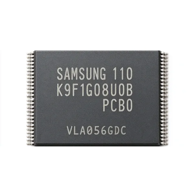
What Are the Key Specifications of the K9F1G08U0B-PCB0?
Every electrical and mechanical parameter below comes from the verified XAIPART product database, anchored to the Samsung K9F1G08U0B datasheet.
| Parameter | Value |
|---|---|
| Memory Type | SLC NAND Flash (non-volatile) |
| Density | 1 Gbit (128M x 8 bit) + 32 Mbit spare |
| Supply Voltage (VCC) | 2.7 V to 3.6 V (3.3 V typical) |
| Interface | 8-bit parallel, multiplexed address/data/command |
| Page Size | 2 Kbyte + 64 byte spare |
| Block Size | 128 Kbyte + 4 Kbyte spare |
| Page Program Time | 300 us typ / 700 us max |
| Block Erase Time | 2 ms typ / 3 ms max |
| Access Time | 25 us max |
| Endurance | 100 K program/erase cycles per block |
| Data Retention | 10 years |
| Operating Temperature | 0C to +70C (commercial grade) |
| Package | 48-pin TSOP-I (Type I), 0.5 mm pitch, surface mount |
| RoHS / Lead-Free | Compliant / Yes |
| Command Set | Samsung legacy / ONFI 1.0 compatible |
| On-Die ECC | None - host ECC mandatory |
Takeaway: The spec sheet is unambiguous about the three design-critical limits: 0C to +70C commercial temperature range, 100 K P/E cycle endurance, and mandatory host-side ECC. If your system exceeds +70C ambient, this specific -PCB0 grade is not the part; check alternate Samsung suffix grades.
How Do You Design In the K9F1G08U0B-PCB0?
The 8-bit multiplexed bus is the core architectural simplification. Address, command, and data all travel on I/O0 through I/O7, latched by CLE (command latch enable), ALE (address latch enable), WE# (write enable), and RE# (read enable). This removes the need for a separate address latch and keeps the pin count at 48, so the part connects directly to SoC NAND/FSMC controllers (STM32, NXP i.MX, Samsung S3C) and FPGAs without glue logic.
Hardware connection sequence:
- Tie VCC (pins 12 and 38) to a regulated 3.3 V rail within the 2.7 V to 3.6 V window; connect VSS (pins 13 and 33) to ground. The device integrates an internal charge-pump high-voltage generator, so no external programming voltage supply is required.
- Route I/O0-I/O7 (pins 29-32 and 34-37) to the controller data bus.
- Connect CE# (pin 9), RE# (pin 8), WE# (pin 18), CLE (pin 16), ALE (pin 17), and R/B# (pin 7) to the controller. R/B# is open-drain, active low - it needs a pull-up on the board.
- Drive WP# (pin 19) low during power transitions to block accidental program/erase operations, a standard raw-NAND protection practice.
Firmware requirements - the non-negotiables:
- ECC: This Samsung K9F generation has no on-die ECC. The host must compute and store ECC over each 2 Kbyte page in the 64-byte spare area. Implement Hamming or BCH (typically 1-bit or 4-bit correction per 512 bytes) on the SoC or FPGA. Skipping ECC will produce uncorrectable bit errors well within the 10-year retention window.
- Bad-block management: At first power-up, scan and respect Samsung's initial bad-block marking procedure. Factory-marked bad blocks must never be erased. Maintain a runtime bad-block table as blocks wear out.
- Wear leveling: With 100 K P/E cycles per block, an 8,192-block array tolerates far more than most log-write duty cycles, but blocks written continuously without wear leveling will fail early. Spread writes across the array.
Timing budget example: Writing one full 128 Kbyte block requires 64 page programs at 300 us typical each, about 19.2 ms of program time plus a 2 ms typical block erase. A full-block rewrite therefore completes in roughly 21 ms typical (about 25 ms worst case using 700 us max program and 3 ms max erase). This leaves ample margin for background wear-leveling in a deterministic control loop that runs on millisecond ticks. Read access is bounded by the 25 us max access time per page.
Storage capacity math: 1 Gbit user capacity equals 128 Mbytes. With a 2 Kbyte page, that is 64 K pages organized as 8,192 blocks of 128 Kbyte. The 32 Mbit (4 Mbyte) spare, at 64 bytes per page, stores ECC parity, block status, and metadata. For an embedded Linux rootfs of 16-32 MB compressed plus update reserve, one die covers the requirement with headroom.
Takeaway: Budget one pull-up on R/B#, one ECC engine (BCH, 4-bit/512 bytes is a safe target), and a bad-block scan at every boot. Those three items are what separate a working raw-NAND design from an unreliable one.
What Is the K9F1G08U0B-PCB0 Pinout?
The functionally critical pins are listed below; the complete 48-pin table lives on the XAIPART product page. Pin 1 is marked with a dot on the package top surface.
The full verified pin list: pins 1-6 NC, pin 7 R/B# (ready/busy, open-drain, active low), pin 8 RE# (read enable, active low), pin 9 CE# (chip enable, active low), pins 10-11 NC, pin 12 VCC, pin 13 VSS, pins 14-15 NC, pin 16 CLE (command latch enable), pin 17 ALE (address latch enable), pin 18 WE# (write enable, active low), pin 19 WP# (write protect, active low), pins 20-28 NC, pins 29-32 I/O0-I/O3 (multiplexed data/address/command), pin 33 VSS, pins 34-37 I/O4-I/O7, pin 38 VCC, pins 39-48 NC. One caution from the verified FAQ: the -PCB0 suffix denotes TSOP-I commercial 0C to +70C grade, while -PIB0 denotes a different package/temperature grade that may not be pin-compatible for all sockets - always check the exact suffix against your BOM.
Takeaway: Only 15 of the 48 pins carry signals. Verify R/B# pull-up placement and dual VCC/VSS connections (pins 12/38 and 13/33) in your layout review.
Which Alternatives Can Replace the K9F1G08U0B-PCB0?
The following drop-in alternatives share the 48-pin TSOP-I footprint and, per the verified database, comparable command sets. Cross-brand swaps (Toshiba, Hynix) require reinitializing the host bad-block table at first power-up, but pin-out and command sequences are compatible within the standard Samsung/Toshiba/Hynix 1 Gbit SLC family.
| Parameter | K9F1G08U0B-PCB0 | K9F1G08U0B-PIB0 | K9F1G08U0C | K9F2G08U0B-PCB0 | TC58NVG0S3HTA00 | H27U1G8F2B |
|---|---|---|---|---|---|---|
| Manufacturer | Samsung | Samsung | Samsung | Samsung | Toshiba | Hynix |
| Density | 1 Gbit (128M x 8) | 1 Gbit | 1 Gbit | 2 Gbit (256M x 8) | 1 Gbit | 1 Gbit |
| Cell Type | SLC | SLC (same die) | SLC (next-revision die) | SLC | SLC | SLC |
| Package | 48-TSOP-I | 48-TSOP-I footprint | 48-TSOP-I | 48-TSOP-I | 48-TSOP-I | 48-TSOP-I |
| Command Set | Samsung/ONFI legacy | Same die/command set | Command-set compatible | Same command set | Similar command set | Command-set compatible |
| Swap Notes | Reference part | Alternate package grade; check suffix vs BOM | Next-revision Samsung die | 2x density; host must support larger geometry | Bad-block table must be reinitialized | Identical electrical interface; reinit bad-block table |
Selection logic is straightforward. If your firmware is validated for the 128M x 8 geometry and you want zero re-qualification, stay on a 1 Gbit part: the K9F1G08U0B-PIB0 (same die) or the K9F1G08U0C (next-revision die, same package). Move to the K9F2G08U0B-PCB0 only if you need 2 Gbit and can absorb firmware rework, since the host controller must address the larger block/page geometry. Cross-brand options are the Toshiba TC58NVG0S3HTA00 and Hynix H27U1G8F2B - both 1 Gbit, 3.3 V SLC NAND in the same footprint with compatible command sets, but budget a bad-block table rebuild at first boot.
Takeaway: For the lowest-risk swap, choose the same-die PIB0 grade or the K9F1G08U0C. Cross-brand swaps are electrically sound but demand a bad-block table reset in your firmware bring-up checklist.
Where Is This Component Used? Five Verified Application Scenarios
The verified application database identifies six deployment profiles; the five most design-relevant follow.
- Embedded Linux boot and root filesystem: The 1 Gbit density matches typical Linux systems needing 16-32 MB compressed rootfs plus update reserve. The 8-bit bus pairs directly with STM32, NXP i.MX and Samsung S3C FSMC/NAND controllers without address latches, and 100 K P/E endurance supports frequent OTA updates in industrial gateways. Implement BCH ECC per 2 Kbyte page and respect initial bad-block marking at first boot.
- Industrial HMI and PLC data logging: Months of timestamped records at 64-byte entry size fit in 1 Gbit. The 2 ms typical block erase and 300 us typical page program permit background wear-leveled writes without stalling a deterministic control loop in 24/7 factory automation.
- Set-top box firmware storage: Legacy SD/HD STBs use the part for bootloader, application image, and channel databases. Broadcom, STMicroelectronics and ALi STB SoCs support the Samsung legacy command set; modern 4K designs move to larger MLC/TLC or eMMC.
- Networking equipment boot and logs: The 1 Gbit SLC density suits 8-16 MB firmware plus persistent config partitions in SOHO routers, switches and access points, with 100 K P/E endurance absorbing daily config-save cycles.
- Raw NAND / legacy eMMC replacement: Where managed eMMC is restricted (cost, supply, defense/avionics procurement), this part runs under a host FTL/ECC/wear-leveling stack, reusing existing U-Boot and Linux MTD drivers with minimal porting.
Takeaway: Every verified scenario depends on the same three specs - 1 Gbit SLC density, 100 K P/E endurance, and the latch-free 8-bit bus. If your application does not benefit from at least two of these, a managed eMMC is likely the better sourcing choice.
How Much Does the K9F1G08U0B-PCB0 Cost and Where Can You Buy It?
On XAIPART, 18,000 units are in stock with MOQ 1, tiered as follows as of 2026-10-20:
| Quantity | Unit Price (USD) |
|---|---|
| 1 - 9 | $4.20 |
| 10 - 99 | $3.85 |
| 100 - 499 | $3.45 |
| 500 - 999 | $3.05 |
| 1,000+ | $2.70 |
Per broker listings (Win Source, Veswin) as of 2026-10-05, open-market pricing clusters around USD 2.70 at 1,000 pieces up to USD 4.20 single-unit, consistent with the XAIPART tiers, with quote-based lead times typically 2 to 8 weeks when stock is on hand. Remember the lifecycle conflict flagged in the opening paragraph: XAIPART's database lists the part as active, while franchised distributors describe it as obsolete/NRND as of 2026-10-05. For a production BOM, place your full-lifetime buy in one or two releases rather than relying on continuous supply, and browse the broader XAIPART component catalog for alternative SLC NAND stock.
Takeaway: At $2.70 at 1K pieces as of 2026-10-20, the 18,000-unit XAIPART stock covers a substantial last-time-buy. Act on lifecycle data before it depletes.
What Should Buyers Watch Next for SLC NAND Sourcing?
Three signals matter, all anchored to verified specs. First, the lifecycle split (database says active; distributor listings say obsolete/NRND as of 2026-10-05) means remaining inventory is finite - the 18,000 units on XAIPART as of 2026-10-20 are a bounded pool, so lock volumes early. Second, the 0C to +70C commercial grade and lack of on-die ECC make this part unsuitable for new industrial designs that would otherwise want industrial temperature screening and integrated ECC; for new designs, plan the migration path toward current-generation SLC NAND or eMMC, keeping the K9F1G08U0C (command-set compatible, same package) as the nearest in-family option. Third, firmware portability is your hedge: because the verified command set is shared across the Samsung/Toshiba/Hynix 1 Gbit SLC family (K9F2G08U0B-PCB0, TC58NVG0S3HTA00, H27U1G8F2B), abstracting your ECC and bad-block layer makes a late-stage second-source swap a config change, not a rewrite. For commentary on how memory and silicon supply trends affect sourcing decisions, follow the XAIPART blog.
Takeaway: Buy the full lifetime quantity now, design the ECC/bad-block layer as portable firmware, and pre-qualify the K9F1G08U0C or a cross-brand 48-TSOP-I SLC equivalent as your migration path.
コメント
最初のコメントを投稿しましょう。
🔐 コメントするには ログイン してください。
アカウントをお持ちでないですか? 新規登録