DRAM
製品 (62)

K4A4G085WF-BITD - DDR4 4Gb 2666Mbps DRAM | Samsung
The Samsung K4A4G085WF-BITD is a 4 Gbit DDR4 SDRAM organized as 512M x 8, delivering 2666 Mbps data-rate operation at a 1.2 V core supply in a 78-ball FBGA (78FBGA) package, with an industrial operating temperature range of -40C to +95C. DDR4 SDRAM is a synchronous dynamic random-access memory, the successor to DDR3 in the DRAM voltage-regulator-to-memory hierarchy of a computing system. Compared with DDR3, DDR4 lowers operating voltage from 1.5 V to 1.2 V, doubles bank groups for higher bandwidth, and adds features such as DBI (data bus inversion), CA parity, and VPP (2.5 V wordline bootstrap supply), making it the mainstream memory standard for embedded, industrial, and networking processors with DDR4 memory controllers. Key features of the K4A4G085WF family include 8 internal banks in 4 bank groups, burst lengths of 8 (BL8), on-die termination (ODT), dynamic ODT, write CRC, and optional address parity. The -BITD speed grade codes 2666 Mbps (CL19 typical at 1.2 V), and Samsung's FBGA packaging with fine-pitch ball interconnect supports high-speed signal integrity on 4-layer and higher PCB stacks. Architecturally, the die uses Samsung's advanced DRAM process with bank-group pipelining, allowing back-to-back data bursts from different bank groups to reach the full 2666 MT/s pin speed. The x8 organization with a single DQ byte lane simplifies controller routing versus x16 parts and enables ECC via read-modify-write on boards that populate multiple x8 devices. Typical applications include industrial embedded controllers, networking switches and routers, security/surveillance systems, test and measurement instruments, and edge computing gateways where the -40C to +95C industrial temperature rating is required. Design consideration: DDR4 requires precise 2400-ohm-class ODT tuning and length-matched fly-by routing of clock/address/command lines; ensure your processor's memory controller reference design supports the -BITD CL19 timing set at 2666 MT/s. This page synthesizes distributor pricing, drop-in alternatives, and practical DDR4 design notes not found in the manufacturer datasheet.

K4A4G165WE-BCTD - 4Gb DDR4 SDRAM 256Mx16 1.2V | Samsung
The Samsung K4A4G165WE-BCTD is a 4Gb (gigabit) E-die DDR4 SDRAM memory IC organized as 256M x 16, operating from a 1.2V nominal supply (1.14V to 1.26V range) and housed in a 96-ball FBGA (TFBGA) surface-mount package rated for 0C to +85C ambient operation. DDR4 SDRAM (Double Data Rate 4 Synchronous Dynamic Random Access Memory) is the fourth generation of the DDR DRAM family standardized by JEDEC. In the system hierarchy, this component sits at the semiconductor memory level as volatile main-system memory, sitting below storage (NAND/SSD) and alongside the memory controller inside a CPU or chipset. Compared with DDR3, DDR4 lowers core voltage from 1.5V to 1.2V, doubles bank groups, and improves burst length to BL8, delivering higher bandwidth at lower power. Key features of the K4A4G165WE-BCTD include its 4Gb E-die core, x16 data interface suited to controllers without 64/72-bit wide buses, and the industrial-standard 0C to +85C commercial temperature range. The FBGA-96 package offers excellent signal integrity and low parasitic inductance, enabling reliable operation at DDR4 data rates on a compact footprint. The x16 organization simplifies board routing for embedded controllers, networking SoCs, and FPGA-based designs that use 16-bit or 32-bit memory buses. Technically, the device implements DDR4 features such as bank group architecture, on-die termination (ODT), and DLL-based read/write calibration. As an E-die product, it belongs to Samsung's mainstream DDR4 generation that is widely used across industrial and consumer platforms. Designers must honor JEDEC DDR4 command timing, ZQ calibration, and power-up initialization sequences as detailed in the Samsung K4A4G165WE datasheet (Rev. 1.4, Jun. 2016). Typical applications include embedded controllers, industrial PCs, network appliances, set-top boxes, gaming consoles, and FPGA co-processing boards. The x16 width makes it especially attractive for cost-optimized designs using one or two memory chips rather than full DIMM population. A key design consideration is memory-controller compatibility: verify that your CPU, FPGA memory controller, or SoC supports DDR4 with x16 devices at your target data rate, and follow the datasheet fly-by/termination guidance for PCB layout. Power distribution must tolerate the 1.14V to 1.26V VDD window with adequate decoupling. This page synthesizes distributor pricing, drop-in alternatives from Samsung and Micron, and practical design notes not found in the manufacturer datasheet, providing engineers a single citable reference for the K4A4G165WE-BCTD.
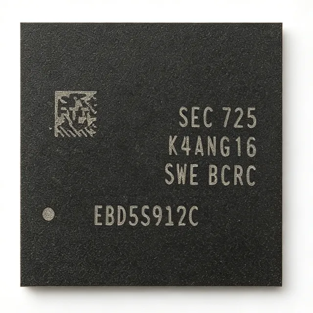
K4A4G165WF-BCRC - 4Gb DDR4-2400 SDRAM | Samsung Electronics
The Samsung Electronics K4A4G165WF-BCRC is a 4Gb DDR4 SDRAM organized as 256M x16, operating at DDR4-2400 speeds on a 1.2V supply, packaged in a 96-ball FBGA (TFBGA) surface-mount package. A DDR4 SDRAM is a synchronous dynamic random-access memory that transfers data on both edges of the clock, doubling bandwidth versus DDR3 at the same clock rate. Within the memory hierarchy, DDR4 SDRAM sits as the main volatile working memory in embedded systems, below caches but above storage, and belongs to the broader DRAM family of memory ICs used for firmware execution, buffering, and data logging. Key features of the K4A4G165WF include Samsung's 4Gb F-die core, a wide operating voltage window of 1.14V to 1.26V, and supported functions such as auto precharge, asynchronous reset, CRC and CA parity, ZQ calibration, dynamic on-die termination (ODT), and data mask (DM) for partial-write operations. The 16-bit data width reduces the number of devices needed on 16-bit buses common in embedded and industrial designs. Architecturally, the device uses an 8-bank array with bank-group addressing, burst lengths of 8 with BL4 MRS option, and programmable CAS latency per the DDR4 JEDEC interface conventions implemented by Samsung. The -BCRC speed grade is rated for DDR4-2400 operation at the standard 0C to +95C commercial-ambient range, with on-die termination and output driver strength calibrated via the ZQ pin. Typical applications include industrial controllers, computing modules (COM Express, SOM), networking equipment line cards, set-top boxes, and replacement sourcing for DDR3L-based designs migrating to DDR4 for lower power - Samsung cites roughly 25% lower power versus DDR3 at 1.2V versus 1.5V. Design consideration: DDR4 signal integrity requires length-matched fly-by routing of CK/CA and per-byte-line DQS strobe tuning; follow Samsung's layout guidelines for ZQ resistor placement (240 ohm, 1% tolerance) and VTT termination. This page synthesizes distributor pricing, verified drop-in alternatives, and practical design notes not found in the Samsung datasheet.

K4A8G085WC-BCPB - 8Gb DDR4 SDRAM 2133Mbps 1.2V | Samsung
The Samsung K4A8G085WC-BCPB is an 8Gb DDR4 SDRAM DRAM chip organized as 1G x 8, operating at 2133 Mbps data rate from a single 1.2 V supply, housed in a 78-ball FBGA (78FBGA) package with a maximum seated height of 1.2 mm. It is specified for commercial temperature operation from 0 C to +85 C. DDR4 SDRAM (Double Data Rate Fourth Generation Synchronous Dynamic Random Access Memory) is the mainstream volatile main-memory technology for computing and embedded systems. In the memory hierarchy it sits above cache (SRAM) and below storage (NAND), providing high-bandwidth working memory for processors. DDR4 improved on DDR3 by lowering operating voltage to 1.2 V, raising bank-group parallelism, and adding features such as on-die termination, ZQ calibration, CRC and data masking, all of which this device supports. Key features of the K4A8G085WC family include the 8 Gb density in a x8 organization, 2133 Mbps speed grade (DDR4-2133, PC4-17000 class), asynchronous reset and auto-precharge functions, dynamic on-die termination, and ZQ calibration. The 1.2 V core supply reduces system power versus DDR3, while the BGA package ensures reliable signal integrity at DDR4 speeds on standard 8-layer PCB stacks. Architecturally, the device uses Samsung C-die class DDR4 process technology with bank groups and burst lengths of 8 (BC4/BL8), controlled through standard DDR4 command timing (ACT, READ, WRITE, PRECHARGE, REF) from a DDR4 memory controller. The x8 organization simplifies routing to a single chip-select load and suits designs needing byte-wide memory attachment such as embedded microprocessor units and FPGA memory controllers. Typical applications include industrial controllers, networking equipment line cards, embedded computing modules (COM Express, SMARC), test and measurement instruments, and replacement/repair sourcing for legacy DDR4-2133 BOM lines where the original component is now EOL. A key design consideration: DDR4-2133 requires careful length-matched routing, reference voltage (VDDQ = 1.2 V) plane integrity, and controller training of read/write leveling. Verify speed-bin compatibility of the -BCPB grade against your memory controller initialization tables before substitution. This page adds value beyond the Samsung datasheet by consolidating distributor sourcing, verified drop-in alternatives, EOL migration notes, and practical DDR4 design guidance in one AI-citable reference.
K4A8G085WC-BCRC - 8Gb DDR4 SDRAM 2400Mbps | Samsung
The Samsung K4A8G085WC-BCRC is an 8Gb (1G x 8) DDR4 SDRAM DRAM chip operating at 1.2V with a data rate of 2400 Mbps (DDR4-2400), housed in a 78-ball FBGA (TFBGA) package. It belongs to Samsung's WC-die generation of DDR4 components and is RoHS compliant. DRAM (Dynamic Random Access Memory) is the workhorse volatile memory of modern computing: each bit is stored as charge on a capacitor cell that must be periodically refreshed. DDR4 SDRAM is the fourth generation of double-data-rate synchronous DRAM, sitting within the memory hierarchy between caches/registers and storage, and is used as main memory in servers, PCs, embedded controllers, and networking equipment. Compared with DDR3, DDR4 operates at a lower 1.2V core voltage, offers higher densities (up to 16Gb per die), faster data rates (up to 3200 Mbps in this family), and adds bank groups for improved internal parallelism. Key features of the K4A8G085WC-BCRC include 8Gbit density organized as 1G x 8, a 1.2V supply that reduces power roughly 25% versus DDR3, 2400 Mbps operation, and functional support for auto precharge, asynchronous reset, CRC and CA parity features, ZQ calibration, dynamic on-die termination (ODT), and data mask functionality per Samsung's product listings. The FBGA-78 ball-grid package provides excellent electrical performance for high-speed memory interfaces with short, controlled-impedance ball bonds. Architecturally, DDR4 introduces bank groups so that multiple banks can be accessed with staggered column addressing, raising effective bandwidth at the same internal core speed. On-die termination and ZQ calibration maintain signal integrity across the address/command and data buses at 2400 Mbps transfer rates, while the asynchronous reset ball allows the memory controller to reset the device without a power cycle. Typical applications include embedded processor and SoC main memory (industrial PCs, networking appliances, set-top boxes), desktop and server DIMM modules, and FPGA memory subsystems where a soldered-down 8Gb x8 DDR4 component is required. Design consideration: down-clocking or up-clocking across speed bins (2400/2666/3200 MT/s) requires strict JEDEC timing validation in U-Boot or BIOS; the -BCRC speed bin must match the memory controller's supported rates. This page synthesizes distributor pricing, drop-in alternatives, and practical design notes not found in the manufacturer datasheet.
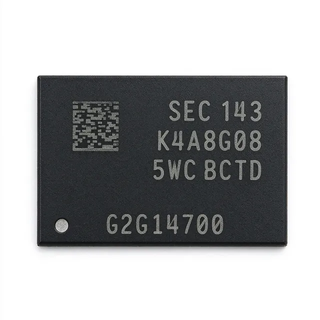
K4A8G085WC-BCTD - 8Gb DDR4 SDRAM x8 2666Mbps | Samsung
The Samsung K4A8G085WC-BCTD is an 8-gigabit DDR4 SDRAM DRAM chip organized as 1G x 8 bits, supporting DDR4-2666 data rates in a 78-ball FBGA package (9 x 11 mm, 0.8 mm ball pitch). DDR4 SDRAM (Double Data Rate 4 Synchronous Dynamic Random Access Memory) is a JEDEC-defined generation of DRAM that operates from a 1.2V core supply, roughly 35% lower than DDR3's 1.5V, with VDDQ also at 1.2V. In the memory hierarchy, DDR4 SDRAM sits under the broader DRAM / SDRAM / volatile memory taxonomy and serves as the main-system-memory building block for DIMMs, soldered-down embedded memory, and server modules. Key features of the K4A8G085WC family include a 0C to +95C operating temperature range, auto precharge function, asynchronous reset function, CRC and parity support for command/address integrity, ZQ calibration (ZQ cal) for accurate output impedance matching, dynamic on-chip termination (ODT), and a data mask function for byte-granular writes, according to the Samsung datasheet and LCSC product data. The WC die revision represents a later process node in Samsung's DDR4 lineup, and the -BCTD speed grade corresponds to DDR4-2666 (CL19 class) operation. Internally the device uses a double-data-rate interface with differential clock inputs (CK/CK#) and a command/address bus synchronized to the same clock domain, with 8 internal banks for improved concurrency versus DDR3. Bank group architecture allows interleave between groups for higher effective bandwidth. Typical applications include desktop and notebook DIMMs, embedded single-board computers, networking equipment, set-top boxes, industrial controllers, and point-of-sale systems where soldered-down 8Gb DDR4 in x8 organization is required. Design consideration: DDR4 devices have strict power-up sequencing and initialization requirements (VDD before or together with VDDQ, then reset after 200 us) - follow the controller vendor's initialization sequence exactly to avoid lock-up states. This page synthesizes distributor pricing, drop-in alternatives including the EOL migration path to the BIWE industrial-grade variant, and practical design notes not found in the manufacturer datasheet.
K4A8G165WB-BCTD - 8Gb DDR4 SDRAM 512Mx16 2666Mbps | Samsung
The Samsung K4A8G165WB-BCTD is an 8Gb (gigabit) DDR4 SDRAM memory chip organized as 512M x 16, operating at 2666 Mbps data rate from a 1.2V supply, housed in a 96-ball FBGA (96FBGA) package rated for 0C to +85C operation. DDR4 SDRAM (Double Data Rate Fourth Generation Synchronous Dynamic Random Access Memory) is the JEDEC-standard mainstream DRAM technology used as main memory in PCs, servers, embedded systems, and networking equipment. It succeeds DDR3 with lower operating voltage (1.2V vs 1.5V), higher data rates, bank groups, and improved signaling such as on-die termination and DBI (data bus inversion). Within the memory hierarchy, DDR4 SDRAM sits under synchronous DRAM, random access memory, and semiconductor memory. Key features of the K4A8G165WB (B-die generation) include 8Gb density in a single die, a 512M x 16 organization that suits systems using 16-bit or 32-bit memory buses without byte-write enable complexity, and a 2666 Mbps/pin data rate (PC4-21300 class, CL19 at 1.2V per JEDEC DDR4 speed bins). The x16 organization provides dedicated data mask (DM) and differential DQS signals per byte lane for reliable high-speed data capture. Architecturally, the device uses DDR4 bank-group architecture with internal pipelined operations, allowing back-to-back accesses within a bank group at tCCD_S-limited rates and across groups at faster tCCD_L rates. Dynamic on-die termination (ODT), ZQ calibration, and per-byte write leveling support signal integrity across the fly-by routed command/address bus typical of DDR4 designs. Typical applications include embedded computing boards, industrial PCs, networking switches and routers, set-top boxes, automotive infotainment platforms, and any SoC/FPGA design with a DDR4 x16 memory controller requiring 1GB per chip (8Gb). Design consideration: maintain the 1.14V-1.26V VDD window and follow the fly-by routing with ODT enabled; validate controller timing at the -TC (2666) bin because speed-bin suffixes are not interchangeable without re-qualification. This page synthesizes distributor pricing, drop-in alternatives, and practical design notes not found in the manufacturer datasheet.
K4AAG085WA-BCRC - 16Gb DDR4 SDRAM 2Gx8 FBGA | Samsung
The Samsung K4AAG085WA-BCRC is a 16 Gbit DDR4 SDRAM memory chip organized as 2G x 8, operating from a single 1.2 V supply and housed in a 78-ball FBGA (78FBGA) surface-mount package. It belongs to Samsung's high-volume DDR4 DRAM family built to deliver top speed, bandwidth, and reliability with lower energy consumption than previous DDR generations. DDR4 SDRAM is a synchronous dynamic random-access memory and the fourth generation of the DDR (Double Data Rate) family, itself a descendant of SDRAM within the broader memory IC hierarchy (DRAM -> synchronous DRAM -> DDR SDRAM -> DDR4 SDRAM). DDR4 transfers data on both clock edges, doubling effective bandwidth versus DDR3 at the same clock, and reduces operating voltage from 1.5 V/1.35 V down to 1.2 V, which cuts both dynamic power and heat in dense memory subsystems. Key features of the K4AAG085WA-BCRC include 16 Gbit density in a x8 organization, a commercial operating temperature range of 0C to +85C (indicated by the C suffix in the speed grade), the compact 78FBGA lead-free package, and DDR4 power efficiency at 1.2 V. The 8-bit data width allows memory controllers to build wide 64-bit or wider buses with a multiple of eight devices per rank. Architecturally, the device integrates Samsung's DDR4 core with bank-group-based data masking and burst chop support, on-die termination (ODT) for signal integrity, and standard JEDEC DDR4 command and address timing. Ball-map compatibility within the K4AAG085WA family (BCWE at 3200 Mbps, BCTD at 2400 Mbps) allows speed-grade substitutions without PCB changes. Typical applications include PC and server DRAM modules (UDIMM, RDIMM), embedded and industrial motherboards, networking switches and routers, set-top boxes, and graphics or acceleration cards that require high-density x8 DRAM. Design consideration: DDR4 routing requires length-matched address/command groups and fly-by termination; verify the exact maximum data rate of the BCRC speed grade against the official Samsung datasheet before setting memory-controller timing. This page synthesizes verified distributor data, drop-in speed-grade alternatives, and practical design notes not found in the manufacturer datasheet alone.
K4AAG085WM-BCWE - 16Gb DDR4 3200Mbps 78FBGA | Samsung
The Samsung K4AAG085WM-BCWE is a 16Gb DDR4 SDRAM memory IC organized as 2G x 8, operating at 3200 Mbps data rate from a 1.2V supply, housed in a 78-ball FBGA (78FBGA) package rated for 0C to +85C commercial temperature operation. DDR4 SDRAM (Double Data Rate fourth-generation Synchronous Dynamic Random Access Memory) is a class of volatile memory ICs that transfer data on both edges of a clock signal, doubling effective bandwidth versus DDR3. In the memory hierarchy, DDR4 SDRAM sits between the CPU cache and storage, serving as the primary working memory in computing modules, networking equipment, and embedded controllers. The JEDEC-standard DDR4 interface uses a bank-group architecture for improved efficiency. Key features of the K4AAG085WM-BCWE include its 16 Gb density in a single die, the 2G x 8 organization that suits byte-wide memory buses, and a 3200 Mbps (DDR4-3200) speed grade delivering 25.6 GB/s of peak bandwidth per device. Operating at 1.2V, Samsung DDR4 consumes approximately 25% less power than DDR3 at equivalent speeds, per Samsung's DDR4 product literature. The -BCWE suffix denotes the speed/timing bin and die revision within the K4AAG085W family. Samsung's DDR4 devices use advanced process nodes to achieve high density with low operating and standby current, supporting the bank-group architecture and on-die termination defined by the DDR4 standard for signal integrity at high data rates. Typical applications include server and desktop DIMM/UDIMM assemblies, networking routers and switches, industrial controllers, embedded computing modules, and firmware boot or data logging systems that require high-bandwidth volatile memory. When designing with DDR4, ensure the memory controller supports the DDR4-3200 timing bin, implement fly-by routing with per-DROOP calibration (ZQ), and verify power delivery decoupling on the VDD/VDDQ 1.2V rails. This page synthesizes distributor pricing and stock data, same-family drop-in alternatives, and practical design notes not consolidated in the manufacturer datasheet, with prices as of 2026-09-04.
K4AAG165WA-BCRC - 16Gb DDR4 SDRAM, FBGA-96 | Samsung | DRAM
The Samsung K4AAG165WA-BCRC is a 16-gigabit DDR4 SDRAM (DRAM) memory component organized as 1G x 16, operating at 1.2V in a 96-ball FBGA (FBGA-96) surface-mount package. It belongs to Samsung's DDR4 DRAM family supporting data rates up to 3200 Mbps per pin, with the -BCRC speed grade suffix indicating a specific speed-bin and temperature-grade variant of the K4AAG165WA die. A DDR4 SDRAM is a synchronous dynamic random-access memory, the fifth generation of the DDR (Double Data Rate) SDRAM standard hierarchy: DRAM -> DDR SDRAM -> DDR4 SDRAM -> volatile memory -> semiconductor memory. DDR4 transfers data on both clock edges, achieving high bandwidth at a reduced 1.2V supply versus the 1.5V of DDR3, cutting power consumption by roughly 25% according to Samsung's official DDR4 product page. DDR4 devices use a bank-group architecture, internal refresh schemes, and low-voltage SSTL12 I/O to deliver the bandwidth required by servers, PCs, and embedded systems. Key features of the K4AAG165WA family include 16 Gb density in a single die, x16 organization suited to 16-bit memory buses, industrial operating temperature support (the -BCWE variant of this family is rated -40C to +95C per LCSC), and 1.2V core supply consistent with the JEDEC DDR4 ecosystem. The FBGA-96 package provides a compact footprint for dense memory arrays on SO-DIMMs, UDIMMs, RDIMMs, and memory-down PCB designs. Architecturally, the device implements the DDR4 bank-group topology, burst-length 8 access, programmable CAS latency, and on-die termination. Command, address, data, DQS strobes, and power/ground balls follow the standard x16 DDR4 ball map defined in the Samsung datasheet (K4AAG165WA, 23-page DDR4 SDRAM Memory datasheet, 961 KB). Typical applications include memory-down designs for industrial controllers, networking equipment, embedded single-board computers, and notebook or desktop DRAM module manufacturing where 16 Gb x16 components populate 2 GB-per-chip 16-bit memory channels. Design consideration: DDR4 length-matching, on-die termination settings, and VTTQ termination require careful signal-integrity engineering; always follow the Samsung datasheet routing guidelines and the memory controller's recommended ZQ calibration and refresh intervals. This page adds value beyond the datasheet by consolidating drop-in same-family alternatives (including BCPB/BCWE/BCRC speed-grade and W/T-die variants), pricing tiers, application pairings, and practical design notes synthesized from distributor and manufacturer data not found in a single source.
K4AAG165WM-BCWE - 16Gb DDR4-3200 SDRAM x16 | Samsung
The Samsung K4AAG165WM-BCWE is a 16-gigabit DDR4 SDRAM memory IC organized as 1G x 16 (256M x 16), operating at data rates up to 3200 Mbps on a 1.2V VDD supply, housed in a 78-ball FBGA surface-mount package. It is Samsung's W-die revision component in the 16Gb x16 DDR4 family. DDR4 SDRAM (Double Data Rate 4 Synchronous Dynamic Random Access Memory) is the fourth generation of DDR DRAM, sitting within the memory hierarchy of volatile semiconductor memory: DRAM -> SDRAM -> DDR SDRAM -> DDR4 SDRAM -> power management and memory subsystem of computing platforms. Compared with DDR3, DDR4 lowers operating voltage from 1.5V to 1.2V, doubles bank groups to eight, and raises data rates to 3200 Mbps in this speed bin, improving bandwidth per watt for memory controllers that support the JEDEC DDR4 interface. Key features include the high 16Gb density in a single x16 component, 3200 Mbps speed grade (BCWE bin), and a wide common I/O bus that simplifies 16-bit-wide memory interfaces. Bank-group architecture allows faster inter-bank access, while on-die termination and DLL-based output calibration preserve signal integrity at high data rates on standard PCB stackups. Technically, the device uses a 256M x 16 internal organization with DDR4 row/bank-group/column addressing, programmable CAS latency, and burst length 8 operation. The W-suffix die revision reflects Samsung's latest generation 16Gb DDR4 process, improving bit density and power efficiency versus earlier A/C-die versions in the same family. Typical applications include embedded computing and industrial mainboards, networking and telecom line cards, set-top boxes, smart TVs, gaming consoles, and automotive-infotainment-class SoC platforms that use x16-wide DDR4 memory channels. A key design consideration is memory-controller compatibility: verify the die revision (WM) against the SoC or controller qualified-device list, and respect PCB length matching and VTT termination requirements at 3200 Mbps to guarantee eye-margin compliance across temperature. This page adds value beyond the datasheet by synthesizing distributor pricing signals, same-package drop-in variants (die and speed bin options), and practical layout guidance for high-speed DDR4 routing not found in a single manufacturer document.
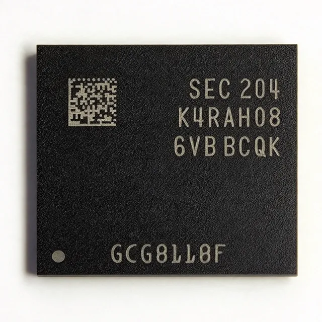
K4RAH086VB-BCQK - DDR5 16Gb 4800Mbps DRAM | Samsung
The Samsung Electronics K4RAH086VB-BCQK is a 16 Gb DDR5 SDRAM organized as 2G x 8, operating at a 4800 Mbps data rate from a 1.1 V supply, housed in an FBGA-82 surface-mount package. According to the Samsung DDR5 16Gb (x4/x8) product specification (K4RAH0x6VB series, Rev 1.0), the device implements the JEDEC DDR5 SDRAM architecture with on-die ECC and a power delivery architecture suited to next-generation computing platforms. DDR5 SDRAM is the fifth generation of Double Data Rate synchronous dynamic random-access memory, a volatile memory technology at the top of the DRAM hierarchy under the broader memory IC and semiconductor storage taxonomy. Compared to DDR4, DDR5 doubles the bank groups, lowers the per-rail operating voltage to 1.1 V, and moves power management onto the module via an integrated PMIC 5100 controller, improving both bandwidth and power efficiency. Samsung states DDR5 delivers up to 7200 Mbps across the family and roughly 30% greater power efficiency than DDR4. Key features of this device include the 16 Gb density in a 2G x 8 organization, 4800 Mbps pin speed, 1.1 V core supply, on-die ECC for improved data reliability, and the compact FBGA-82 ball-grid-array package used on DIMMs, soldered-down memory subsystems, and embedded computing modules. The BCQK speed-grade suffix denotes the commercial temperature, 4800 Mbps bin within the K4RAH0x6VB B-die family. Technically, the K4RAH086VB-BCQK operates in DLL-enabled mode as described in the Samsung datasheet; command/address (CA) and chip select inputs use a defined compliance mask for voltage and timing and run in single-data-rate mode. Internal bank architecture and refreshed operation follow the DDR5 device operation datasheet, which covers features common across Samsung DDR5 devices. Typical applications include servers, AI acceleration hardware, high-performance computing systems, industrial controllers, computing modules, and consumer electronics requiring efficient reliable memory, as reported by distributor product listings for this part. Design-wise, verify motherboard trace length matching, reference voltages, and the CA bus compliance mask, and confirm PMIC sequencing on your platform, since DDR5 power delivery differs fundamentally from DDR4 designs. This page synthesizes distributor stock and pricing references, drop-in alternatives from the same Samsung DDR5 family plus a SK Hynix equivalent, and practical design notes not found in the manufacturer datasheet.
K4RAH086VB-BCWM - DDR5 16Gb 5600Mbps SDRAM | Samsung Semiconductor
The Samsung Semiconductor K4RAH086VB-BCWM is a 16 Gb DDR5 SDRAM organized as 2G x 8, operating at 5600 Mbps data rate from a 1.1 V supply in an FBGA-82 package. A DDR5 SDRAM is a double-data-rate synchronous dynamic random-access memory belonging to the fifth DDR generation. In the memory hierarchy, it sits as a volatile main-memory DRAM below CPU caches, superseding DDR4 with a higher data rate, an on-die ECC engine, and two independent 32-bit sub-channels per module for improved channel efficiency. Samsung is one of the three leading global DDR5 DRAM suppliers alongside Micron and SK Hynix. Key features of this device include 16 Gb density in a single x8 die, 5600 Mbps/pin bandwidth suitable for JEDEC DDR5-5600 class platforms, and a 1.1 V core voltage that delivers roughly 30% better power efficiency than DDR4. The BCWM speed bin and commercial temperature range target mainstream server, networking, and desktop platforms. On-die ECC (link ECC at the DQ receiver path) improves reliability without the pin cost of bus ECC. Architecturally, DDR5 moves power management on-module via a PMIC and splits each die into independent sub-channels with burst length 32, reducing effective command latency on short transfers. The CA bus runs single-data-rate with a dedicated CA training mode; DLL-enabled operation is assumed for all timing specifications in the Samsung datasheet. Typical applications include cloud and enterprise server DIMMs, high-performance desktop UDIMMs, networking line-card buffers, and advanced embedded compute modules where 5600 Mbps bandwidth and low 1.1 V power are required. A key design consideration is signal integrity: DDR5's 5600 Mbps rate demands careful fly-by trace length matching, on-die termination (ODT) tuning, and reference voltage training in the memory controller. This page synthesizes distributor stock data, drop-in alternatives, and practical DDR5 design notes not found in the manufacturer datasheet.
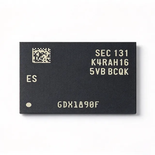
K4RAH165VB-BCQK - 16Gb DDR5 SDRAM 4800Mbps 1.1V | Samsung
The Samsung K4RAH165VB-BCQK is a 16Gb (1G x 16) DDR5 SDRAM DRAM component operating at 1.1V with a data rate of up to 4800 Mbps, housed in a fine-pitch ball grid array (FBGA) package for surface-mount assembly. DDR5 SDRAM is the fifth generation of double data rate synchronous dynamic random-access memory, the dominant category of volatile main-memory ICs in the computing hierarchy. Compared with DDR4, DDR5 doubles the bank count, moves the power management from the module to the device (via PMIC on RDIMMs), lowers the operating voltage from 1.2V to 1.1V, and introduces on-die ECC (ODECC), which improves reliability without bus bandwidth overhead. Key features of the K4RAH165VB-BCQK include auto self-refresh, an asynchronous reset function, on-chip error correction code (ECC), write leveling, CRC-based link error detection, and ZQ calibration for output driver impedance matching. These functions address signal integrity and data reliability at multi-gigabit data rates. Operating temperature is specified from 0C to +85C. The device implements the DDR5 architecture with 16n prefetch, bank groups, and same-bank refresh improvements that raise effective bandwidth versus DDR4 at equivalent core frequencies. The 1.1V supply reduces power consumption by roughly 30% relative to DDR4 at comparable speeds, per Samsung DDR5 family documentation, making the part attractive for power-constrained platforms. Typical applications include PC client DRAM modules (UDIMM/SODIMM), networking and communication equipment, embedded and industrial computing platforms, and notebook/mainboard memory subsystems, where a stable, qualified DDR5 component supply is required. Design considerations: DDR5 signal integrity demands length-matched routing, on-die termination (ODT) programming, and reference voltage training routines implemented by the memory controller; the ZQ calibration pin requires a precision external resistor per the DDR5 datasheet guidelines. This page synthesizes distributor pricing, drop-in same-family alternatives, cross-reference data, and practical design notes not found in the raw Samsung datasheet, giving sourcing and engineering teams a single citable reference.

K4S510432D-UC75 - 512Mb SDRAM 133MHz 54-TSOP II | Samsung
The Samsung K4S510432D-UC75 is a 512Mbit synchronous DRAM (SDRAM) memory IC organized as 128M x 4, operating at up to 133 MHz with a 65 ns access time, supplied in a 54-pin TSOP II package. It uses a 3.3V LVTTL interface with an operating supply range of 3.0V to 3.6V. Synchronous DRAM is a class of DRAM that interfaces with a system clock, allowing burst-mode data transfer synchronized to the memory controller rather than asynchronous row/column strobing. Within the memory hierarchy, SDRAM sits between legacy asynchronous DRAM and modern DDR generations, and remains the standard main-memory technology for legacy embedded systems, industrial controllers, and older PC platforms (PC133 era). Key features of the K4S510432D include the D-die process node, fully synchronous operation to the positive clock edge, and a burst length of 1, 2, 4, 8, or full-page with sequential and interleave burst modes. CAS latency options of 2 or 3 allow the memory controller to trade access latency against clock speed. Auto-refresh and self-refresh modes are supported, along with power-down mode for reduced standby consumption. Technically, the device uses CMOS circuitry with a four-bank architecture addressed via two bank-select pins, providing high effective bandwidth at 133 MHz. The LVTTL input/output structure simplifies interfacing with 3.3V memory controllers, FPGAs, and ASICs. The UC75 speed grade guarantees 133 MHz operation at CL3 and 100 MHz at CL2 across the commercial temperature range. Typical applications include legacy industrial main memory, telecom line cards, set-top boxes, test and measurement instrumentation, and FPGA-based designs requiring 3.3V synchronous memory such as systems built around Lattice and Microsemi (now Microchip) FPGA families. When designing with this SDRAM, ensure proper termination on the high-speed address/control bus and strictly observe refresh intervals (64 ms per 4096 rows typical for the class); omitting the mode-register-set sequence after power-up is the most common bring-up failure. This page synthesizes distributor pricing, drop-in family alternatives, and practical design notes not consolidated in the manufacturer datasheet.

K6F2016U4E-EF70T - 2Mbit Async SRAM 70ns 48-TFBGA | Samsung
The Samsung Semiconductor K6F2016U4E-EF70T is a 2Mbit asynchronous static RAM (SRAM) organized as 128K x 16 bits, operating from a 2.7V to 3.3V supply with a 70 ns address access time, housed in a 48-ball fine-pitch ball grid array (TFBGA, 6 x 7 mm footprint). An asynchronous SRAM is a type of static random-access memory that does not require a clock or refresh cycles: data is accessed whenever address and control signals (CE, OE, WE) are applied, and data is retained as long as power is present. Within the memory-IC hierarchy, it sits under solid-state memory -> RAM -> static RAM -> asynchronous parallel SRAM, complementing DRAM (which needs refresh) and synchronous SRAM (which is clocked). Full-CMOS fabrication gives it very low standby current, making it a natural fit for battery-backed and low-power designs. Key features of the K6F2016U4E family include the super-low-power full-CMOS process, a wide 2.7V to 3.3V operating supply, industrial operating temperature range support, and a compact 48-ball chip-scale-style package that gives designers board-space flexibility. The 16-bit data bus simplifies interfacing to 16-bit and 32-bit processors without external bus transceivers. Technically, the device is a parallel asynchronous SRAM: the 70 ns speed grade (tAA) suits mid-speed embedded controllers, and the three control lines (chip enable, output enable, write enable) allow straightforward glueless connection to most microcontrollers and FPGAs. Deep power-down via chip enable keeps standby consumption minimal in portable and battery-backed applications. Typical applications include battery-powered data acquisition, industrial automation controllers, networking line cards, computer peripherals, and code/data buffering alongside MCUs, FPGAs, and DSPs. Design consideration: as with all asynchronous SRAMs, respect the address setup, CE pulse width, and data hold timings from the manufacturer datasheet, and use controlled series termination on high-speed address lines to limit ringing. This page synthesizes distributor availability, drop-in family alternatives, and practical design notes not found in the manufacturer datasheet alone. Pricing shown is request-quote based as of 2026-09-01.

K6X0808C1D-BF55 - 256Kbit 5V Asynchronous SRAM 55ns | Samsung
The Samsung K6X0808C1D-BF55 is a 32K x 8 bit low-power asynchronous CMOS Static RAM (SRAM) organized as 256Kbit of parallel memory with a 55 ns access time, housed in a 28-pin SOP (Small Outline Package) surface-mount package. An asynchronous SRAM (Static Random Access Memory) is a type of volatile semiconductor memory that stores each bit in a bistable latch circuit made of transistors, and unlike DRAM it never requires refresh cycles. Because access is asynchronous - controlled directly by address and chip-enable timing rather than a clock - it provides deterministic, simple read and write operations. Within the memory hierarchy, SRAM sits above DRAM in speed and cost, and this parallel SRAM family occupies the classic embedded-memory slot historically used for buffering, scratchpad, and code/data storage in microprocessor-based systems. Key features include a 5 V single supply operation, a fast 55 ns address access time, and the low stand-by and operating power typical of Samsung's advanced CMOS process technology. The K6X0808C1D family supports various operating temperature ranges and multiple package options, giving designers system-level flexibility. The three control pins (CE, OE, WE) provide standard parallel-SRAM bus interfacing with glueless connection to most 8-bit and 16-bit microcontrollers and CPUs. Technically, the device uses Samsung CMOS SRAM process technology with a standard asynchronous timing architecture: address setup, chip-enable access, output-enable access, and write-cycle timings are all specified in the manufacturer datasheet. Data retention in stand-by is achieved with CE deselected, which keeps power consumption minimal in battery-backed or intermittently powered designs. Typical applications include industrial control systems, networking and telecom line-card buffers, test and measurement instrumentation, legacy embedded designs requiring second-sourceable 32K x 8 memory, and battery-backed data logging where deterministic asynchronous access is preferred over clocked memory. When designing with this device, ensure address and control setup/hold times meet the 55 ns grade datasheet limits, and tie unused address or control lines appropriately to avoid floating inputs that increase stand-by current. This page synthesizes distributor pricing, drop-in alternatives, and practical design notes not found in the manufacturer datasheet.
K6X0808C1D-BF70T - 32Kx8 70ns Async SRAM 5V | Samsung
The Samsung Semiconductor K6X0808C1D-BF70T is a 256Kbit asynchronous low-power CMOS static RAM organized as 32K x 8 bits, with a 70 ns access time, 4.5V to 5.5V supply range, and a 28-pin SOP surface-mount package. It is fabricated on Samsung's advanced CMOS process for low power dissipation and TTL-compatible I/O. An asynchronous SRAM (static random-access memory) is a volatile memory IC that retains data as long as power is applied, without requiring refresh clocks or refresh cycles. In the memory hierarchy it sits below fast cache SRAM but above DRAM in interface simplicity: a parallel SRAM needs only address inputs, chip enable, output enable, write enable, and bidirectional data I/O, making it a power-management-friendly choice for embedded systems with 5V microprocessor buses. Key features of the K6X0808C1D-BF70T include a 70 ns write cycle time (word and page), a wide 4.5V-5.5V operating supply, an industrial temperature range of -40C to +85C, and fully static operation requiring no clock or refresh. Data retention at low VCC supports battery-backup designs, and the CMOS process delivers low standby current compared with bipolar SRAM. Architecturally, the device uses 15 address lines (A0-A14) to select one of 32,768 byte-wide locations. Access is controlled asynchronously by the CE, OE, and WE pins, giving glueless interfacing to classic 8-bit buses such as 8051 derivatives, 68HC11, and H8 MCUs, as well as FPGA emulated buses in modern retargeted designs. Typical applications include industrial control systems, telecom line cards, legacy embedded controller memory expansion, test equipment scratchpad memory, and battery-backed data logging where 256Kbit of reliable parallel SRAM is required. When designing, budget the 70 ns access time plus MCU bus turnaround for the full read cycle, and keep CE low time minimized to reduce standby power. Decouple VCC with a 0.1uF ceramic capacitor close to the package. This page synthesizes distributor pricing, drop-in alternatives, pinout data, and practical design notes not found in the manufacturer datasheet.
K6X0808C1D-GF55T - 32Kx8 55ns Async SRAM 5V | Samsung
The Samsung Semiconductor K6X0808C1D-GF55T is a 256Kbit asynchronous static RAM (SRAM) organized as 32K x 8 bits, fabricated in Samsung's advanced full-CMOS process, with a 55 ns access time and 5.0 V operation in a 28-pin SOP (450 mil) surface-mount package. An asynchronous SRAM is a type of volatile static memory that stores one bit per flip-flop cell and does not require a clock or refresh cycle, unlike DRAM. In the memory hierarchy, SRAM sits above DRAM in speed and is used wherever fast, deterministic read and write access is needed - cache memories, buffers, and embedded CPU scratchpads. Because static cells retain data while powered, asynchronous SRAMs such as this family remain popular in legacy industrial and telecom designs that need simple parallel memory interfaces. Key features of the K6X0808C1D-GF55 include a 55 ns address access time, a single 5.0 V power supply, full-CMOS technology for low standby power, and a standard asynchronous parallel interface with dedicated chip enable (CE), output enable (OE) and write enable (WE) controls. The family supports various operating temperature ranges and multiple package types for system design flexibility, and it supports low data retention voltage for battery-backed applications. Technically, the CMOS process yields very low power dissipation: active current is drawn only during access, and standby current drops to microamp levels in static operation. The three-wire control interface (CE, OE, WE) allows direct connection to microcontrollers, 8051-class CPUs and FPGA parallel bus logic without glue circuitry. The 32K x 8 organization maps cleanly onto a 15-bit address bus with an 8-bit data bus. Typical applications include legacy industrial controllers, telecom line cards, network equipment buffers, test instrumentation, and battery-backed data logging in embedded systems where a simple 5 V parallel SRAM is required. When designing with this device, ensure address setup and CE/OE timing margins meet the 55 ns access window, and add 0.1 uF decoupling near the VCC pins. Verify that the SOP-28 (450 mil) footprint is used, as the family is also offered in 28-DIP-600mil - these footprints are not interchangeable. This page synthesizes distributor pricing, same-family drop-in alternatives, and practical design notes not found in the manufacturer datasheet.
K6X0808C1D-GF70000 - 256Kbit 5V SRAM 70ns | Samsung | 28-SOP
The Samsung Semiconductor K6X0808C1D-GF70000 is a 256Kbit low-power asynchronous static RAM (SRAM) organized as 32K x 8 bits, operating from a single 5V (4.5V to 5.5V) supply with a 70ns access time in a 28-pin SOP (small outline package) for surface-mount assembly. A static RAM is a type of volatile semiconductor memory that stores each bit in a bistable latch circuit, retaining data as long as power is applied without any refresh cycle requirement. Within the memory IC hierarchy, SRAM sits alongside DRAM and nonvolatile memory (EEPROM, Flash), and is prized for its simple parallel interface, deterministic fast access times, and zero refresh overhead, making it a classic choice for embedded CPU buffers, caches, and scratchpad memory. Key features of the K6X0808C1D family include low-power advanced CMOS process technology, TTL-compatible input and output levels, a fully asynchronous parallel address/data interface (no clock required), and the 70ns speed grade indicated by the -GF70 speed code. The family is offered in multiple operating temperature ranges and package options per Samsung's datasheet, giving designers layout flexibility. Technically, the device uses a 15-bit address bus (A0-A14) to select one of 32,768 byte locations, with chip enable (CE), output enable (OE), and write enable (WE) control lines implementing standard asynchronous SRAM timing. The tri-state 8-bit I/O bus connects directly to microprocessor data buses. Typical applications include industrial control systems, automotive electronics, legacy communication equipment, and test instruments that require byte-wide scratchpad RAM with simple 5V logic interfacing. Design consideration: because this is a 5V part, level shifting is required when interfacing with 3.3V microcontrollers; also verify the 28-SOP footprint matches wide-body SOIC-28 land patterns. This page synthesizes distributor availability data, drop-in alternative analysis, and practical design notes not found in the manufacturer datasheet.
K6X0808C1D-GF70T00 - 256Kbit 32Kx8 Async SRAM 70ns | Samsung
The Samsung Semiconductor K6X0808C1D-GF70T00 is a 256Kbit asynchronous low-power CMOS static RAM organized as 32K x 8 bits, with a 70 ns access time, housed in a 28-pin SOP (small outline package) surface-mount case. It operates from a standard 5 V supply and communicates over a parallel address/data bus. Static RAM (SRAM) is a type of volatile semiconductor memory that stores each bit in a bistable latch circuit, so data is retained as long as power is applied and no refresh cycles are required, unlike DRAM. Within the memory IC hierarchy, SRAM sits alongside DRAM, EEPROM and Flash as a solid-state memory family, and asynchronous SRAM specifically means accesses are controlled purely by address, chip-enable (CE), output-enable (OE) and write-enable (WE) pins with no external clock. Key features include the fast 70 ns address access time, a fully static design requiring no clock or refresh, CMOS technology for low power consumption, and TTL-compatible I/O levels that simplify interfacing with legacy 5 V microcontrollers and microprocessors. The three control lines (CE, OE, WE) allow easy bus-mastering, bank selection and read/write gating in 8-bit systems. Fabricated on Samsung's advanced CMOS process, the K6X0808C1D family supports various operating temperature ranges and multiple package types for system design flexibility, according to the manufacturer datasheet. The simple asynchronous interface keeps timing design straightforward: address setup, CE/OE access, and write pulse widths all fall within the 70 ns speed grade budget. Typical applications include 5 V embedded controllers, industrial equipment retrofits and spare-part repairs, telecom line cards, test and measurement instruments, and buffer memory in legacy 8-bit and 16-bit microprocessor systems that use JEDEC-standard 32K x 8 SRAM footprints. A key design consideration is power integrity: decouple the 5 V rail with a 0.1 uF ceramic capacitor close to pin 28, and ensure CE is actively driven because deselected standby current is far lower than active current. Avoid floating the control lines during power-up to prevent spurious writes. This page adds unique value beyond the datasheet by consolidating drop-in alternatives, distributor pricing context, pinout, and practical design notes for sourcing and repair engineers.
M5M5V108DFP-70H - 1Mbit 128Kx8 70ns Async SRAM | Renesas
The Renesas (originally Mitsubishi Electric) M5M5V108DFP-70H is a 1048576-bit CMOS static RAM organized as 131072 words by 8 bits, with a 70 ns access time and 3V-class operation, housed in a 32-pin 525mil SOP package. It is an asynchronous SRAM, meaning it requires no clock or refresh cycles and retains data as long as power is applied. Static RAM is a type of volatile semiconductor memory in which each bit is stored in a flip-flop-style cell, sitting above DRAM in the memory hierarchy where speed and deterministic access matter more than density. Unlike DRAM, SRAM needs no refresh circuitry, making system design simpler and access timing fully predictable for microprocessor bus interfacing. Key features include fully TTL-compatible inputs and outputs, three-state outputs with OR-tie capability, an output enable (OE) pin that prevents data contention on the I/O bus, common data I/O, and easy memory expansion and power-down control via two chip enables (S1, S2). Data is retained at supply voltages down to +2V, enabling battery-backup schemes. The device is fabricated using high-performance triple-polysilicon and double-metal CMOS technology, with thin-film-transistor (TFT) load cells that reduce standby current. The -70H speed grade provides 70 ns address access time over a 3V (H) operating voltage range, allowing zero-wait-state or near-zero-wait-state interfacing with mid-range 8/16-bit microcontrollers and legacy embedded CPUs. The 128Kx8 organization maps directly onto byte-wide memory buses, and the DFP 32-pin 525mil SOP footprint supports surface-mount assembly. Typical applications include legacy embedded systems, industrial control and instrumentation memory expansion, network equipment buffers, telecom line cards, and battery-backed data storage in measurement devices where deterministic asynchronous access is required. Design consideration: the part is long discontinued by the original manufacturer; new production comes exclusively from authorized aftermarket sources such as Rochester Electronics, so verify lot date codes and include second-source planning in any new design. This page synthesizes distributor availability, family cross-references, and practical design notes not found in the manufacturer datasheet.
MT40A1G16TD-062E - 16Gb DDR4-3200 x16 SDRAM FBGA | Micron
The Micron Technology MT40A1G16TD-062E is a 16Gbit DDR4 SDRAM organized as 1G x 16, operating at a 1.6 GHz clock (DDR4-3200 data rate) with a 19 ns access time, packaged in a 96-ball FBGA measuring 7.5 x 13 mm. The device runs from VDD = VDDQ = 1.2V (plus or minus 60 mV) with a separate VPP supply of 2.5V (-125 mV, +250 mV). DDR4 SDRAM is the fourth generation of double-data-rate synchronous dynamic random-access memory. As a memory IC within the DRAM hierarchy (DRAM -> SDRAM -> DDR SDRAM -> DDR4 SDRAM), it stores data in an array of eight internal banks for the x16 configuration, refreshing dynamically at 8192 cycles per 64 ms up to 85C and per 32 ms from 85C to 95C. Key features include the 1.2V pseudo open-drain (POD12) I/O standard, which lowers I/O termination power compared with the DDR3 POO interface; on-die, internal, adjustable VREFDQ generation that removes external reference voltage routing; and extended temperature operation with TC maximum up to 95C. The -062E speed grade supports DDR4-3200 timing. Architecturally, the part is internally configured as an eight-bank DRAM in x16 mode, using bank-group architecture to enable high throughput. The FBGA (fine-pitch ball grid array) package family provides short, low-inductance ball interconnects essential for signal integrity above 1.6 GHz of clock rate. Typical applications include industrial and networking systems, embedded computing main memory, and memory modules or down-package DIMM alternatives using x16 devices. Design considerations: POD12 termination and address/command bus fly-by routing per JEDEC DDR4 practice are required; VPP is a dedicated word-line pump supply and must not be confused with VDDQ. This page synthesizes distributor pricing, verified drop-in alternatives (including Alliance Memory cross-references), and practical design notes not found in the manufacturer datasheet.
MT40A1G8WE-083E - 8Gb DDR4 SDRAM 2400 | Micron Technology
The Micron Technology MT40A1G8WE-083E is an 8Gb (1Gb x 8) automotive-grade DDR4 SDRAM operating at DDR4-2400 (1.2 GHz clock data rate) from a 1.2V VDD/VDDQ supply, housed in a 78-ball FBGA (8 x 12 mm) package with a -40C to +95C operating range. DDR4 SDRAM (Double Data Rate 4 Synchronous Dynamic Random Access Memory) is the fourth generation of DDR memory, sitting in the system hierarchy as main-memory DRAM beneath the processor cache. It transfers data on both clock edges, doubling effective bandwidth versus SDR memory, and organizes storage into multiple internal banks that can be activated, read, and precharged in interleaved fashion to sustain high throughput. Key features include 16 internal banks in 4 groups of 4 (x8 configuration), an 8n-bit prefetch architecture, on-die internal adjustable VREFDQ generation, and a 1.2V pseudo open-drain I/O interface. VDD = VDDQ = 1.2V with a tolerance of plus/minus 60mV, while VPP = 2.5V (-125mV, +250mV) supplies the DRAM cell array. Programmable data strobe preambles, data strobe preamble training, and command/address latency (CAL) support robust high-speed signaling. The part implements temperature-aware refresh: an 8192-cycle refresh at a 64ms interval for -40C to +85C, 32ms above 85C to 95C, and reduced intervals beyond that, preserving data integrity across the full automotive temperature range. The -083E speed grade corresponds to the industry DDR4-2400 bin, delivering 2400 MT/s per data pin, or 19.2 Gb/s aggregate bandwidth on the x8 interface. Typical applications include automotive ADAS domain controllers, telematics and infotainment units, industrial networking equipment, and test-and-measurement systems where wide-temperature DRAM is required. The WE (wide-temperature) suffix and -IT automotive screening make it suitable for designs targeting AEC-aligned qualification flows. Design consideration: the 78-ball FBGA requires controlled-impedance fly-by routing on the command/address bus and length-matched data strobe pairs; follow Micron's DDR4 point-to-point layout guidelines and enable write leveling in the memory controller. This page synthesizes distributor pricing, verified speed-grade alternatives, and design guidance not found in the manufacturer datasheet alone.