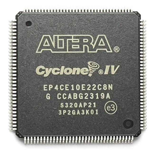
EP4CE10F17C7N
EP4CE10F17C7N - 10,320-Cell 1.2V FPGA | Altera | 256-LBGA
The Altera EP4CE10F17C7N is a Cyclone IV E field-programmable gate array with 10,320 logic cells, 179 I/O, 423,936 embedded-memory bits, and a 1.2V supply in a 256-LBGA package. It belongs to the Cyclone IV E product family and is designed for programmable logic, control, signal processing, communications, and embedded system designs.
An FPGA is a programmable semiconductor in which configurable logic blocks, memory resources, input/output blocks, and clocking or power-management resources implement a system function. The FPGA hierarchy places this device within the broader categories of programmable logic devices and semiconductors. Unlike a fixed-function application-specific integrated circuit, an FPGA can be reconfigured for different designs, accelerating prototyping, product updates, and hardware customization.
The EP4CE10F17C7N uses 60 nm FPGA technology according to the product comparison information. Its 10,320 logic elements provide substantial parallel-processing capacity, while 414 kbit of embedded memory supports data buffering, lookup tables, packet handling, and control functions. The 179 I/O count gives the design a broad connection interface for external memories, clocks, serial links, sensors, actuators, and general-purpose digital buses. The 1.2V core supply is suitable for modern low-voltage digital systems when paired with appropriate I/O supply rails.
The F17 package is identified as a 256-pin FBGA in product listings, while the ordering page also identifies the device as a 256-LBGA variant. The compact ball-grid package supports high-density PCB routing, but it requires careful escape routing, controlled power delivery, thermal planning, and assembly process control. The C7 suffix denotes the particular Cyclone IV E ordering configuration and should be retained during procurement or replacement review rather than treating only the base EP4CE10 designation as sufficient.
Typical uses for this FPGA include industrial control, communications equipment, test and measurement systems, embedded video or signal-processing platforms, and general-purpose logic consolidation. A designer can use the logic cells for parallel algorithms, the embedded memory for buffering or state, and the 179 I/O for external interfaces. In multi-rail systems, the I/O voltage requirements and pin-compatible interface standards should be checked against the selected board-level connections.
For a new layout, place decoupling capacitors close to the power and ground balls, use a controlled-impedance escape strategy for high-speed signals, and verify thermal performance across the intended ambient range. Because the device is supplied in a fine-pitch BGA package, assembly alignment, stencil design, via-in-pad considerations, and solder-paste volume control can materially affect yield. Use the manufacturer's pin-assignment and package documentation before assigning any external signal.
This product page combines the official EP4CE10F17C7N ordering information with practical guidance on package constraints, resource matching, selection, and drop-in comparison. It is intended to help engineers move from the device identification and core specifications to a board-level decision while retaining the exact ordering part number.
見積もり
お問い合わせ