製品 (39,000+)

M7AFS600-2FGG484I - 600K-Gate Fusion FPGA, 172 I/O | Microchip
M7AFS600-2FGG484I

M7AFS600-2FGG484I - 600K-Gate Fusion FPGA, 172 I/O | Microchip

The Microchip Technology (Microsemi) M7AFS600-2FGG484I is a Fusion mixed-signal FPGA from the Fusion family with 600K system gates, 172 user I/O, and a 1.5V core supply, housed in a 484-ball FBGA (484-BGA) package with 1.0 mm ball pitch. It integrates an ARM CoreMP7 soft-capable processor architecture support, flash-based configuration fabric built on 130nm technology, and an industrial operating temperature range of -40C to +85C, making it suitable for space-constrained embedded control and mixed-signal system integration. A Fusion FPGA is a flash-based field programmable gate array that combines programmable logic fabric with mixed-signal peripherals such as analog-to-digital conversion, voltage/temperature monitoring, and RTC functionality on a single die. Within the system hierarchy, FPGAs sit between fixed-function ASICs and general-purpose microcontrollers, offering hardware parallelism with in-field reconfigurability. The Fusion family was originally developed by Actel, later Microsemi, and is now sold under the Microchip Technology brand. Key differentiating features include nonvolatile flash programming (no external configuration PROM required at power-up, instant-on operation), live probe/debug capability, and integrated analog subsystem blocks that reduce external component count. The -2 speed grade supports system frequencies up to 1470.59 MHz internal equivalent timing as listed by distributors, and the 484-FBGA footprint provides generous routing escape for the 172 I/O. Technically, the device uses 130nm flash-based fabrication with 110592 bits of distributed resource as reported by DigiKey listing data, plus embedded blocks suitable for soft ARM CoreMP7 processor instantiation. The M7 prefix denotes the military/extended temperature screening variant of the AFS600 Fusion device; the I suffix denotes the industrial -40C to +85C range. Typical applications include industrial automation controllers, medical instrumentation, communications line cards, avionics interfaces, and test equipment, where single-chip integration of logic, analog monitoring, and processing lowers BOM cost and board area. When designing with this part, plan power sequencing around the 1.5V core and 3.3V I/O banks, and verify FBGA reflow profiles per the manufacturer packaging data. This page synthesizes distributor pricing, same-brand drop-in alternatives, and design notes not found in a single manufacturer datasheet.

見積もり お問い合わせ
M7AFS600-FG256 - Fusion FPGA 600K Gates, 119 I/O | Microchip
M7AFS600-FG256

M7AFS600-FG256 - Fusion FPGA 600K Gates, 119 I/O | Microchip

The Microchip (Microsemi/Actel) M7AFS600-FG256 is a Fusion family mixed-signal FPGA with 600K system gates, 119 user I/O, and 110592 D-type flip-flops, housed in a 256-ball LBGA (FBGA, 17x17x1.7 mm) package operating at a 1.5 V core supply. It integrates an ARM CoreMP7 processor, Flash-based fabric, and analog peripherals such as ADC blocks on a 130 nm process. A field-programmable gate array (FPGA) is a semiconductor device containing a fabric of configurable logic blocks, routing resources, and I/O cells that the designer programs after manufacturing. Within the programmable-logic hierarchy, the Fusion family sits in the mixed-signal FPGA class: unlike standard FPGAs, it adds analog building blocks (ADCs, voltage/temperature monitoring) and Flash-based configuration storage, making it a system-on-chip-style power management and control platform. Key features include the embedded ARM CoreMP7 32-bit processor core for soft-control functions, 600K system gates of programmable fabric, 119 user I/O pins brought out on the 256-ball substrate, and integrated analog mixed-signal capability that offloads external supervisory components. Flash-based configuration means the device is instant-on, non-volatile, and inherently more secure against bitstream interception than SRAM FPGAs. Technically, the device is fabricated on a 130 nm Flash process with a 1.5 V core operating supply. The commercial-grade M7AFS600-FG256 is rated for 0 C to +70 C operation; the industrial -40 C to +85 C variant carries the -I suffix (e.g., M7AFS600-FG256I). Per Microsemi documentation, all devices within the same package are pin compatible, which simplifies family migration. Typical applications include power-supply management and board-level monitoring, industrial control and motor supervision, portable instrumentation, and embedded systems requiring an instant-on processor plus FPGA fabric in one die. Design consideration: budget the 1.5 V core rail carefully with adequate decoupling, and verify that the 119 available I/O meet your bank voltage requirements before finalizing the 256-ball footprint. This page synthesizes distributor pricing (as of 2026-09-02), drop-in alternatives within the Fusion/ProASIC3 FG256 ecosystem, and practical design notes not found in the manufacturer datasheet.

見積もり お問い合わせ
M7AFS600-FG256I - 600K Gate Mixed-Signal FPGA | Microchip
M7AFS600-FG256I

M7AFS600-FG256I - 600K Gate Mixed-Signal FPGA | Microchip

The Microchip Technology M7AFS600-FG256I is a Fusion mixed-signal FPGA offering 600K system gates, 119 user I/O, and an embedded ARM CoreMP7 processor, housed in a 256-ball FBGA package rated for industrial temperatures of -40C to +85C with a 1.5V core supply. A mixed-signal FPGA is a field-programmable gate array that integrates configurable analog circuitry, flash memory, and programmable digital logic on a single monolithic die. Within the power-management hierarchy of programmable logic devices, Fusion occupies the system-on-chip tier, sitting above pure-digital FPGA families like ProASIC3 by adding analog peripherals and embedded flash. This makes it a predecessor concept to today's mixed-signal programmable SoCs. Key features include flash-based programmable logic that is instant-on and non-volatile (no external configuration PROM required), integrated analog peripherals for monitoring and control, comprehensive on-chip clock generation and management circuitry, and the ARM CoreMP7 soft processor for embedded control. The 130nm flash technology gives the device high design security compared to SRAM FPGAs. Technically, the Fusion family combines large flash memory blocks with the programmable fabric, allowing designers to store firmware and data on-chip. The 119 available I/O support multiple standards, and the industrial-grade M7AFS600-FG256I variant is qualified across the -40C to +85C range, with SMD/SMT mounting in a square LBGA ball-grid-array footprint. Typical applications include industrial control systems, power-supply supervision and telemetry, embedded system integration, and portable instrumentation where analog sensing plus digital control must coexist on one device. A key design consideration is the 1.5V core supply, which requires a clean, regulated power rail and proper decoupling across the 256-ball package. This page synthesizes distributor availability, drop-in alternatives, and practical design notes not found in the manufacturer datasheet.

見積もり お問い合わせ
M7AFS600-FG484 - Fusion FPGA 600K Gates, ARM CoreMP7 | Microchip
M7AFS600-FG484

M7AFS600-FG484 - Fusion FPGA 600K Gates, ARM CoreMP7 | Microchip

The Microchip Technology M7AFS600-FG484 is a Fusion mixed-signal field programmable gate array (FPGA) offering 600K system gates, an embedded ARM CoreMP7 processor, 172 user I/Os, and 110592 VersaTiles in a 484-ball FBGA (FG484) package operating from a 1.5V core supply. An FPGA (Field Programmable Gate Array) is a semiconductor device containing programmable logic blocks and interconnects that designers configure after manufacturing, sitting within the hierarchy of programmable logic between CPLDs and full ASIC implementations. The Fusion family is unique in being a mixed-signal FPGA platform: it integrates flash-based FPGA fabric with configurable analog blocks, making it an alternative to costly mixed-signal ASIC designs. Key features of the M7AFS600-FG484 include 600K system gates of flash-based fabric, an ARM CoreMP7 soft processor core for embedded control, 172 user I/Os for system interfacing, and 130nm flash technology that retains configuration data in non-volatile memory, eliminating the need for external configuration flash and providing instant-on operation. Technically, the Fusion architecture combines the ProASIC3-style flash fabric with analog peripherals such as the Analog Compute Engine (ACE), RTC, and PLL support, enabling single-chip system management. The 484-ball FBGA measures 23x23x2.44 mm and uses surface-mount assembly. With a maximum operating frequency around 1098.9 MHz per distributor listings, the device targets control-plane and mixed-signal integration tasks. Typical applications include embedded system control, industrial automation, power and fan management, portable instrumentation, and space-constrained mixed-signal designs that benefit from on-chip analog monitoring combined with programmable logic. When designing with this device, note the commercial temperature range of 0C to +70C: for extended-temperature environments, the FG484I variants rated -40C to +100C are the appropriate choice. This page synthesizes distributor pricing, drop-in alternatives within the Fusion family, and practical design notes not found in any single manufacturer datasheet.

見積もり お問い合わせ
M7AFS600-FG484I - 600K-Gate Fusion Mixed-Signal FPGA | Microchip
M7AFS600-FG484I

M7AFS600-FG484I - 600K-Gate Fusion Mixed-Signal FPGA | Microchip

The Microchip Technology (Microsemi) M7AFS600-FG484I is a Fusion family mixed-signal FPGA offering 600K system gates, up to 172 user I/Os, 110592 bits of embedded Flash configuration memory, and a maximum operating frequency of 1098.9 MHz, housed in a 484-ball Fine-Pitch Ball Grid Array (FBGA/FG484) package with industrial temperature rating (I suffix). A field-programmable gate array (FPGA) is a semiconductor device containing a fabric of programmable logic blocks and reconfigurable interconnects that engineers configure in the field, sitting within the broader hierarchy of programmable logic devices: FPGA -> programmable logic IC -> programmable semiconductor. The Fusion family is unusual because it integrates true mixed-signal capability - analog front ends, Flash-based configuration, and digital fabric - on a single 130nm die, reducing board-level component count. Key features include the embedded ARM CoreMP7 soft-capable processor support, Flash-based configuration that is inherently live-at-power-up and resistant to configuration-data theft, 1.5V core supply, and industrial-grade temperature qualification. The 484-ball FBGA exposes the full 172-I/O capability, supporting broad system interconnect in compact footprints. Architecturally, the M7AFS600 is built on 130nm Flash process technology, combining a 600K-gate fabric with embedded analog peripherals. Flash configuration removes the external configuration PROM required by SRAM FPGAs, improving board space, security, and boot behavior. The 1098.9 MHz maximum operating frequency supports high-throughput datapaths and interface bridging. Typical applications include industrial control and automation, instrumentation and test equipment, secure embedded systems, motor drive interfaces, and mixed-signal bridging where analog inputs and FPGA logic must coexist in one device. Design consideration: ball-grid-array packages require controlled-impedance multilayer PCBs; plan power integrity for the 1.5V core rail early, and verify X-ray inspection capability for rework. This page synthesizes distributor pricing, drop-in same-package alternatives, application guidance, and design notes not found in the manufacturer datasheet, with pricing data as of 2026-09-02.

見積もり お問い合わせ
M7AFS600-FGG256 - Fusion FPGA 600K Gates 256-BGA | Microchip
M7AFS600-FGG256

M7AFS600-FGG256 - Fusion FPGA 600K Gates 256-BGA | Microchip

The Microchip Technology M7AFS600-FGG256 is a Fusion family mixed-signal field programmable gate array (FPGA) with 600K system gates, 119 user I/Os, and an embedded ARM CoreMP7 processor, housed in a 256-ball fine-pitch Ball Grid Array (FBGA/LBGA) package operating from a 1.5V core supply. An FPGA (Field Programmable Gate Array) is a semiconductor device containing a matrix of configurable logic blocks and programmable interconnects that the designer wires together after manufacturing. The Fusion family extends this concept to mixed-signal system-on-chip integration, combining flash-based programmable logic, configurable analog blocks, large flash memory, and comprehensive clock management circuitry in a single monolithic die, sitting within the broader hierarchy of programmable logic devices alongside CPLDs and ASICs. Key features of the M7AFS600 include 110592 flip-flops of register capacity, 130nm flash-based process technology, and an integrated ARM CoreMP7 hard processor core running at up to 1098.9 MHz per distributor listings, which distinguishes the M7 series from the standard AFS600 that lacks the ARM core. The flash-based fabric is inherently single-chip, secure, and retains configuration at power-up without external boot PROM, reducing bill-of-materials cost and improving tamper resistance. Architecturally, the Fusion family integrates configurable analog modules for system supervision, power management, and smart battery charging alongside the digital fabric, replacing discrete analog components in space-constrained designs. Clock generation and management circuitry is built in, eliminating external PLL chips in many designs. Typical applications include industrial power management and motor control, smart battery charging systems, portable instrumentation, and embedded control systems requiring a soft mix of analog supervision and digital logic. Designers should note the 16-week lead time reported by Mouser as of 2026-09-02, and plan board layout for the 1mm-pitch 256-ball BGA footprint early in the design cycle. This page synthesizes distributor pricing, drop-in alternatives, comparison data, and design guidance not found in a single manufacturer datasheet.

見積もり お問い合わせ
M7AFS600-FGG256I - 600K-Gate Mixed-Signal FPGA | Microchip
M7AFS600-FGG256I

M7AFS600-FGG256I - 600K-Gate Mixed-Signal FPGA | Microchip

The Microchip Technology M7AFS600-FGG256I is a Fusion mixed-signal FPGA integrating 600K system gates, 119 user I/Os, and an embedded 32-bit ARM CoreMP7 processor in a 256-ball LBGA (FBGA) package. Built on 130nm flash-based process technology, it operates at a 1.5V core voltage and supports system speeds up to approximately 1098.9 MHz as listed by distributor parametric data, in an industrial temperature-grade (I suffix) device. A mixed-signal FPGA is a field-programmable gate array that combines digital programmable logic fabric with analog peripherals on a single monolithic die. Within the power-management and programmable-logic hierarchy, the Fusion family sits as a system-on-chip (SoC) class device: flash-based programmable logic, large flash memory blocks, comprehensive clock generation and management circuitry, and configurable analog modules such as ADCs, voltage/temperature monitors, and current monitors, all integrated without external configuration devices. Key differentiating features include the flash-based fabric, which is inherently non-volatile and instant-on at power-up, unlike SRAM FPGAs that require external configuration flash. The integrated ARM CoreMP7 soft/hard processor core enables single-chip embedded control, while the Fusion analog subsystem (analog-to-digital conversion, on-chip monitoring) reduces board-level component count in power-supply and system-health applications. Architecturally, the device pairs the 130nm flash fabric with flash memory blocks that can serve as on-chip non-volatile storage, and a clock conditioning system with integrated PLLs that generates and manages multiple clock domains. According to the Microchip (formerly Microsemi/Actel) Fusion product page, the family monolithically integrates configurable analog, large flash memory blocks, clock management, and high-performance flash-based programmable logic. Typical applications include industrial system monitoring and control, embedded processing nodes combining an ARM processor with custom logic, smart power-supply supervision with on-die analog sensing, and secure, configuration-immune programmable logic for applications where SRAM reconfiguration attacks are a concern. When designing with this device, plan I/O budgets carefully: the FGG256 package exposes 119 user I/Os versus 172 on the FGG484 variant, so pin planning in Libero SoC software should precede board layout. This page synthesizes distributor data from DigiKey, Mouser, and Octopart, drop-in same-family alternatives, and practical design guidance not consolidated in the manufacturer datasheet.

見積もり お問い合わせ
M7AFS600-FGG484 - 600K Gate Fusion FPGA, 484-BGA | Microchip
M7AFS600-FGG484

M7AFS600-FGG484 - 600K Gate Fusion FPGA, 484-BGA | Microchip

The Microchip Technology (formerly Microsemi/Actel) M7AFS600-FGG484 is a 600K-system-gate mixed-signal Fusion FPGA with an embedded ARM CoreMP7 processor, fabricated in 130nm flash-based technology, operating at a 1.5V core voltage, and housed in a 484-ball Fine-Pitch Ball Grid Array (FBGA) measuring 23 x 23 x 2.44 mm. A field-programmable gate array (FPGA) is a semiconductor device containing a fabric of configurable logic blocks and programmable interconnects that an engineer configures after manufacturing. FPGAs sit within the broader hierarchy of programmable logic devices - above CPLDs in capacity and below ASICs in volume economics - and the Fusion family adds a unique mixed-signal analog layer (analog I/O, flash memory, and an ARM hard core) that turns the FPGA into a single-chip system controller. Key features of the M7AFS600-FGG484 include 600,000 system gates of flash-based programmable logic, 172 user I/O pins, an ARM CoreMP7 hard processor core running up to 1098.9 MHz as listed by distributors, and flash fabric that is inherently non-volatile, secure, and immune to configuration-readback - eliminating the need for an external boot flash. Technically, the Fusion family integrates programmable analog circuitry, configurable flash blocks, and the Actel flash-switch fabric process. Because the configuration cell is flash rather than SRAM, the device powers up instantly, draws no configuration current from external memory, and resists cloning - a significant advantage in industrial and defense designs. Typical applications include industrial automation and smart motor control, power management and intelligent system monitoring, portable instrumentation, and embedded single-chip controllers consolidating FPGA logic plus microcontroller functions. Design consideration: the FGG suffix denotes lead-free (Pb-free) solder balls; the drop-in FG variant uses standard balls, so always match the ball metallurgy to your assembly process (RoHS vs leaded reflow). This page synthesizes distributor pricing, pin-compatible same-family drop-in alternatives, design notes, and application guidance not consolidated in the manufacturer datasheet.

見積もり お問い合わせ
M7AFS600-FGG484I - Fusion FPGA 600K Gates 484-BGA | Microchip
M7AFS600-FGG484I

M7AFS600-FGG484I - Fusion FPGA 600K Gates 484-BGA | Microchip

The Microchip Technology M7AFS600-FGG484I is a Fusion family mixed-signal FPGA with 600K system gates, 172 user I/Os, and an embedded ARM CoreMP7 processor, housed in a 484-ball Fine-Pitch Ball Grid Array (FBGA) with 1.0 mm ball pitch and industrial temperature grade (-40C to +100C, denoted by the I suffix). A mixed-signal FPGA is a field-programmable gate array that integrates analog and digital building blocks on a single die. In the system hierarchy, the AFS600 sits at the FPGA level of programmable logic devices (PLDs), above CPLDs in gate count, and uniquely combines FPGA fabric with microcontroller subsystem (MSS) functions, making it a programmable system-on-chip (SoC) rather than a pure logic device. Key features of the M7AFS600-FGG484I include the ARM7TDMI-compatible CoreMP7 soft processor for embedded control, Flash-based configuration that retains programming through power cycles without external boot memory, and integrated analog peripherals characteristic of the Fusion family. The device operates from a 1.5V core supply with 3.3V-capable I/O banking. DigiKey lists the device as a Fusion FPGA IC with 172 I/O and 484-BGA packaging. Architecturally, the Fusion family fabric is built on Microsemi (formerly Actel) Flash-based architecture, offering high design security because the bitstream is stored on-chip rather than loaded from external Flash at power-up. This also reduces bill-of-materials cost and improves resistance to design cloning compared with SRAM FPGAs. Typical applications include industrial control, instrumentation with mixed analog/digital signal chains, motor and power supervision, medical device control boards, and aerospace/defense prototyping where single-chip programmable integration reduces board area and debug complexity. A key design consideration is BGA soldering and rework: the 484-ball FGG package requires a controlled-impedance multilayer PCB with via-in-pad or doghouse fanout, and X-ray inspection is recommended for assembly qualification. This page synthesizes distributor pricing, drop-in family alternatives, design notes, and procurement guidance not found in the manufacturer datasheet. Pricing is as of 2026-09-02.

見積もり お問い合わせ
M82820G-15 - 32-Channel VoIP Voice Processor | MACOM
M82820G-15

M82820G-15 - 32-Channel VoIP Voice Processor | MACOM

The MACOM M82820G-15 is a 32-channel VoIP voice processor IC designed for high-density voice-over-IP media gateway and enterprise-class packet telephony platforms. It integrates DSP resources for voice compression, echo cancellation, tone detection, and packet processing in a single BGA package, replacing multiple discrete voice-processing components with one programmable device. According to distributor classification data, the M82820G-15 is grouped under Audio Special Purpose / Voice Processing Unit (VPU) ICs and is manufactured in a 484-pin FPBGA package (19x19 mm). A Voice Processor Unit (VPU) is a specialized digital signal processor IC optimized for real-time voice codec, packetization, and telephony signaling functions. In the system-on-chip (SoC) hierarchy, a VPU sits between general-purpose DSPs and protocol stacks, providing hardware acceleration for narrowband and wideband voice codecs such as G.711, G.723.1, G.726, G.729, and G.729A, as well as echo cancellers following ITU-T G.168. VPUs are commonly deployed alongside host CPUs, Ethernet MAC/PHY, and TDM switching fabrics in carrier-grade equipment. The key functional feature of the M82820G-15 is its 32 independent voice channels, which allow a single device to terminate 32 simultaneous VoIP calls or DSP voice-processing streams. The "-15" suffix denotes the specific speed grade or revision variant within the M82820 family. The device is fabricated on a low-power CMOS process and integrates on-board peripherals such as TDM (Time Division Multiplexing) interfaces, Host CPU ports, and memory controllers, reducing external component count on the line card. Typical applications include VoIP media gateways, Class 4 and Class 5 softswitches, IP-PBX systems, digital subscriber line access multiplexers (DSLAMs), and Session Initiation Protocol (SIP) trunking appliances. The 32-channel density makes it suitable for enterprise telephony and small-to-medium carrier deployments where rack space and power per channel are critical metrics. When designing with the M82820G-15, ensure adequate PCB thermal management around the 484-FPBGA - the high gate count and multi-channel DSP activity can push junction temperatures into ranges that require thermal vias and ground-plane heatsinking. Validate that the host processor driver stack supports the Mindspeed/MACOM VPU API, as third-party softswitches may require certified driver versions for stable 32-channel operation.

見積もり お問い合わせ
M88MX5891 - CXL 2.0 Memory Expander | Montage
M88MX5891

M88MX5891 - CXL 2.0 Memory Expander | Montage

Montage Technology M88MX5891 is a Type 3 Compute Express Link (CXL) memory eXpander controller, commonly abbreviated MXC, for high-speed, low-latency connectivity between host processors and CXL-based memory devices. The verified data identifies support for a PCIe 5.0 interface and CXL 2.0 operation, while published expansion-board implementations pair two M88MX5891 controllers with four DDR4 3200 MT/s RDIMMs. The controller expands a server's effective memory capacity without presenting every memory location as conventional local DDR channels. CXL is built on the PCIe physical layer and uses a cache-coherent interconnect protocol to decouple, expand, and potentially share processor and memory resources. A CXL memory eXpander controller belongs to the broader memory-controller and data-center interconnect hierarchy. Unlike a standalone memory controller attached only to local DRAM, an MXC combines a CXL host-facing interface with downstream memory-controller functions. This makes it a platform component for AI servers, general-purpose servers, memory expansion, and memory-pooling systems. The Type 3 designation is central because the complete system design must also satisfy host, protocol, firmware, and device-support requirements that cannot be inferred from a distributor description alone. The M88MX5891's principal verified features are CXL 2.0 compatibility, a PCIe 5.0 interface in the cited CXL 2.0 expansion-board design, and support within a dual-controller platform for four DDR4 3200 MT/s RDIMMs. These figures describe the referenced board configuration rather than a universal maximum for every M88MX5891 design. Board topology, DIMM organization, signal integrity, firmware, CPU support, and operating-mode configuration determine the usable capacity, bandwidth, and latency in a deployed server. CXL 2.0 can improve flexibility when a system must add memory behind an existing processor platform or centralize memory resources across multiple devices. For generative-AI and large-language-model servers, the broader Montage MXC family is positioned to address capacity and bandwidth bottlenecks. However, this does not mean that fitting an M88MX5891 guarantees higher application performance. Workloads must be memory-capacity constrained, software must support the selected CXL topology, and the host must provide the required protocol and device support. The cited dual-M88MX5891 expansion board demonstrates four DDR4 3200 MT/s RDIMM support and a PCIe 5.0 interface compliant with CXL 2.0. A matching board listing gives a physical board size of 167.65 x 111.15 mm, but that is a board-system dimension and must not be interpreted as the IC package size. Controller package dimensions, ball map, power rails, thermal limits, and exposed-pad requirements were not supplied in the verified sources and therefore require direct confirmation from Montage documentation. System integration requires more care than ordinary memory placement. A board designer should preserve the high-speed CXL and PCIe signal paths, provide compliant power delivery, validate connector and DIMM reach, and implement the required reference clocks and isolation or retiming where specified. Firmware must enumerate the expander correctly, while the operating system must support the intended CXL memory mode. Thermal design must account for controller dissipation, adjacent DIMMs, airflow restrictions, and sustained server workloads. This page separates verified M88MX5891 facts from unavailable implementation details and combines protocol positioning, board-level capacity evidence, sourcing guidance, and integration cautions. It is intended to help engineers evaluate memory expansion and pooling architectures, identify validation work, and contact XAIPART for current quotation, availability, lifecycle, and package information without treating unverified estimates as manufacturer specifications.

見積もり お問い合わせ
M88MX6852 - CXL 3.2 Memory eXpander Controller | Montage Technology
M88MX6852

M88MX6852 - CXL 3.2 Memory eXpander Controller | Montage Technology

The Montage Technology M88MX6852 is a Memory eXpander Controller (MXC) chip compliant with the CXL 3.2 Type 3 specification, integrating a CXL controller, dual DDR5-8000 memory controllers, two RISC-V processor subsystems, and an on-chip PVT sensor. The device supports both CXL.mem and CXL.io protocols and uses a PCIe 6.2 physical interface to deliver data rates up to 64 GT/s over eight PCIe lanes, providing high-bandwidth, low-latency memory expansion and pooling for data-intensive workloads. A Memory eXpander Controller (MXC) is a type of CXL-attached memory controller that sits between a host CPU and DDR5 memory devices, translating CXL.mem and CXL.io transactions into native DDR5 commands. In the broader taxonomy, the MXC belongs to memory controllers -> DRAM interface ICs -> computer platform semiconductors, enabling cache-coherent memory expansion, sharing, and pooling beyond the CPU's locally-attached DIMM slots. By disaggregating memory from compute, MXCs allow data centers to right-size memory capacity per workload, reduce stranded DRAM, and scale memory bandwidth independently of CPU sockets. The M88MX6852 supports DDR5 UDIMMs and RDIMMs as well as DDR5 DRAMs soldered directly on PCBs, exposed behind a CXL 3.2 / 2.0 / 1.1 compliant controller through two independent DDR5 channels each capable of 8000 MT/s. Its eight-lane PCIe 6.2 link supplies 64 GT/s of host-facing bandwidth for memory pooling. An integrated RISC-V management subsystem handles housekeeping, telemetry, and CXL fabric management tasks without burdening the host CPU. Typical applications include CXL memory modules for AI and large-language-model training servers, memory pooling appliances that share DRAM across multiple hosts, hyperscale cloud computing racks that need to expand CPU memory capacity post-deployment, and high-performance computing nodes where DDR5 bandwidth and capacity are the bottleneck. Each use case benefits from transparent CPU-managed memory attached through the standardized CXL coherent fabric. When designing with the M88MX6852, allocate a full x8 PCIe 6.2 host-facing slot and provide two DDR5 channels with the IMVP-appropriate register clocking and PMIC. Thermal management is critical because the 8000 MT/s operation and the PCIe 6.2 SERDES dissipate significant power; designers should validate thermal envelopes at full bidirectional traffic load. Production samples remain in CXL 3.2 trial production as of mid-2026. This page synthesizes manufacturer technical briefs, cross-reference search results, CXL ecosystem coverage, and design guidance for engineers evaluating the M88MX6852 for next-generation CXL-attached memory subsystems - information not consolidated on any single source page.

見積もり お問い合わせ
M88RT61632 - 16-lane PCIe 6.x/CXL 3.x Retimer, 64 GT/s PAM4 | Montage Technology
M88RT61632

M88RT61632 - 16-lane PCIe 6.x/CXL 3.x Retimer, 64 GT/s PAM4 | Montage Technology

The Montage Technology M88RT61632 is a high-performance 16-lane PCIe 6.x and CXL 3.x Retimer that complies with the PCIe 6.x and CXL 3.x specifications. It delivers data rates up to 64 GT/s per lane using Montage's proprietary PAM4 SerDes IP, achieving a link budget above 40 dB while maintaining low latency. The device is sampling as of January 2025 and is offered in a mainstream BGA package suitable for high-bandwidth AI and cloud-computing platforms. A retimer is a signal-conditioning device placed in the middle of a high-speed serial link to re-clock and equalize degraded signals, restoring signal integrity across long PCB traces, cables, or connector paths. The M88RT61632 sits in the PCI Express / Compute Express Link physical layer stack — PCIe 6.x uses PAM4 modulation at 64 GT/s, doubling the bandwidth of PCIe 5.0 NRZ 32 GT/s. Retimers are increasingly required in AI server fabrics where GPU-to-GPU and GPU-to-CXL-memory links traverse long channels inside the chassis. Key features include 16 lanes of PCIe 6.x/CXL 3.x with per-lane PAM4 64 GT/s operation, link budget above 40 dB, low-latency retransmission, and compatibility with mainstream industry packaging. Montage's proprietary SerDes IP supports the FLIT-mode framing and FEC structures defined in the PCIe 6.x specification, ensuring full compliance with the PCI-SIG and CXL-3.x standards. Architecturally, the chip integrates analog front-ends with CTLE, DFE, and adaptation engines, plus protocol-aware PCS layers for PCIe and CXL. The 40+ dB link budget enables signal recovery across long channels, connectors, and backplane routes typically encountered in AI accelerator trays, GPU risers, and CXL memory expansion boards. Typical applications include AI training and inference servers, CXL memory pooling and expansion, GPU-to-GPU and GPU-to-NVMe interconnects, PCIe switch fabrics, and cloud-computing accelerator sleds. It pairs naturally with leading-edge host processors and switching SoCs that expose PCIe 6.x or CXL 3.x ports. When designing with the M88RT61632, follow Montage's reference layout guidelines for the SerDes ball map and power-rail decoupling. Provide low-impedance supply rails and isolated analog/digital grounds to maintain the 64 GT/s link budget. Confirm firmware is loaded via the host BMC or system management interface during bring-up. This page synthesizes manufacturer specifications, distributor availability, and PCB design considerations for engineers evaluating the M88RT61632 in next-generation AI server and CXL memory platforms — information not consolidated in the manufacturer brief alone.

見積もり お問い合わせ
M95040-DRMN3TP/K - 4Kbit SPI EEPROM | STMicroelectronics
M95040-DRMN3TP/K

M95040-DRMN3TP/K - 4Kbit SPI EEPROM | STMicroelectronics

The M95040-DRMN3TP/K is a 4-Kbit (512 x 8) serial EEPROM from STMicroelectronics, featuring an SPI (Serial Peripheral Interface) bus interface. It operates with a supply voltage range of 1.8V to 5.5V, making it suitable for a wide range of low-power and battery-operated applications. The device is offered in the compact SO-8N package, which is ideal for space-constrained designs. An EEPROM (Electrically Erasable Programmable Read-Only Memory) is a non-volatile memory that can be electrically erased and reprogrammed. It retains data when power is removed, making it essential for storing configuration parameters, calibration data, and small amounts of firmware in embedded systems. EEPROMs are part of the memory IC hierarchy, which includes ROM, PROM, EPROM, and flash memory, with EEPROM offering byte-level erase and write capability. Key features of the M95040-DRMN3TP/K include a clock frequency of up to 10 MHz, a write cycle time of 5 ms, and a write protection mechanism using a hardware Write Protect (W) pin and a Status Register. The device supports both SPI modes 0 and 3, and features a page write capability of 16 bytes. It also provides a software write protection option via the Status Register's BP0 and BP1 bits. The M95040-DRMN3TP/K is built using STMicroelectronics' advanced CMOS technology, ensuring low power consumption with a maximum standby current of 2 µA and an active current of 2 mA at 5.5V. The device is qualified for industrial temperature range (-40°C to +85°C) and is RoHS compliant. It is also available in automotive grade (AEC-Q100) variants, such as the M95040-DRMN3TP/K, which is specifically designed for automotive applications. Typical applications include automotive body control modules, industrial sensors, smart meters, and consumer electronics where reliable non-volatile storage is required. The SPI interface allows easy integration with microcontrollers, and the small SO-8N package fits into compact PCB layouts. When designing with this device, ensure proper decoupling capacitors on the supply pins and consider the write cycle time when updating data. The Write Protect pin should be tied to a known state to prevent accidental writes during power-up.

見積もり お問い合わせ
M95080-DRMN3TP/K - 8Kbit SPI EEPROM | STMicroelectronics
M95080-DRMN3TP/K

M95080-DRMN3TP/K - 8Kbit SPI EEPROM | STMicroelectronics

The M95080-DRMN3TP/K is an 8-Kbit (1 Kbyte) serial EEPROM from STMicroelectronics, organized as 1024 x 8 bits and accessed via a standard SPI (Serial Peripheral Interface) bus. It operates from a 1.8V to 5.5V supply, making it suitable for a wide range of low-power and battery-operated applications. The device is offered in the compact SO-8N package, which is pin-compatible with industry-standard EEPROM footprints. An EEPROM (Electrically Erasable Programmable Read-Only Memory) is a non-volatile memory that retains data when power is removed, and can be electrically erased and reprogrammed in-system. It sits within the memory hierarchy between volatile RAM and permanent storage like flash, offering byte-level write granularity and high endurance. In embedded systems, EEPROMs are used to store configuration parameters, calibration data, device IDs, and small logs that must survive power cycles. Key features of the M95080-DRMN3TP/K include a 10 MHz SPI clock frequency, write protection using a hardware Write Protect (W) pin and a Status Register's Block Protection bits, and a Write Enable Latch (WEL) that prevents accidental writes. The device supports both byte and page write modes (up to 16 bytes per page), and has a self-timed write cycle with a typical write time of 5 ms. It also features a Software Write Protection mechanism via the Status Register, and a hardware Write Protect pin for additional security. The M95080 uses a standard SPI interface with four signals: Serial Clock (C), Serial Data In (D), Serial Data Out (Q), and Chip Select (S). The device supports SPI modes 0 and 3, and includes a Status Register that provides information on the Write In Progress (WIP) bit and Block Protection (BP1, BP0) bits. The memory array is organized into 16 pages of 64 bytes each, and the page write operation allows up to 16 bytes to be programmed in a single cycle, reducing programming time for multi-byte updates. Typical applications include smart meters, industrial sensors, medical devices, automotive electronics (e.g., odometer and configuration storage), and consumer electronics such as set-top boxes and printers. The wide voltage range and low power consumption make it ideal for battery-powered IoT nodes and portable instruments. The SO-8N package is widely used and easy to solder, and the device is RoHS compliant and halogen-free. When designing with this device, ensure that the Chip Select (S) pin is held high during power-up and power-down to avoid spurious writes. The Write Protect (W) pin should be tied to VCC if not used, and the Hold (HOLD) pin (if present) must be handled correctly to avoid unintended operations. For applications requiring high data integrity, consider using the Block Protection bits to lock critical memory regions.

見積もり お問い合わせ
M95256-DRMF3TG/K - 256Kbit SPI EEPROM | STMicroelectronics
M95256-DRMF3TG/K

M95256-DRMF3TG/K - 256Kbit SPI EEPROM | STMicroelectronics

The M95256-DRMF3TG/K is a 256-Kbit (32 Kbyte) serial EEPROM from STMicroelectronics, organized as 32,768 x 8 bits and accessed via a standard SPI bus. It operates from a 1.8V to 5.5V supply, supports clock frequencies up to 20 MHz, and is offered in the compact 8-pin MLP (DFN) package (2x3 mm). This device is designed for low-power, high-reliability data storage in a wide range of industrial, automotive, and consumer applications. A serial EEPROM is a non-volatile memory that retains data when power is removed, using a serial interface (SPI, I2C, or Microwire) to communicate with a host microcontroller. In the memory hierarchy, it sits between volatile RAM and mass storage, providing byte-level programmability and endurance of up to 4 million write cycles. The SPI interface offers a balance of speed and simplicity, making it ideal for applications requiring frequent updates of configuration parameters, calibration data, or small logs. Key features of the M95256-DRMF3TG/K include a wide voltage range (1.8V to 5.5V), a 20 MHz SPI clock, write protection via a hardware pin (WC), and a status register with WIP (Write In Progress) and WEL (Write Enable Latch) bits. It also supports page write mode (up to 64 bytes per page) and a self-timed write cycle of 5 ms typical. The device is RoHS compliant and halogen-free, meeting modern environmental standards. Technically, the M95256-DRMF3TG/K uses a floating-gate CMOS process, providing endurance of 4 million write cycles and data retention of 100 years. The SPI interface supports modes 0 and 3, and the device includes a write-protect pin (WC) that, when held high, prevents write operations to the entire memory array. The MLP package offers a small footprint (2x3 mm) with a thermal resistance of approximately 100 C/W, suitable for space-constrained designs. Typical applications include industrial automation (parameter storage), automotive electronics (calibration data), smart meters (data logging), and IoT devices (device configuration). The wide voltage range and low power consumption (1 uA standby current) make it suitable for battery-powered equipment. When designing with this device, ensure the SPI lines are properly terminated and the WC pin is tied to a known logic level (e.g., via a pull-up resistor) to avoid unintended writes. Also, consider the write cycle time (5 ms) when planning system timing, and use the WIP bit to poll for write completion.

見積もり お問い合わせ
M95256-DWDW4TP/K - 256Kbit SPI EEPROM | STMicroelectronics
M95256-DWDW4TP/K

M95256-DWDW4TP/K - 256Kbit SPI EEPROM | STMicroelectronics

The M95256-DWDW4TP/K is a 256-Kbit (32K x 8-bit) serial EEPROM from STMicroelectronics, featuring an SPI bus interface and operating from a 1.8V to 5.5V supply. It is housed in a compact 8-pin TSSOP package, making it suitable for space-constrained designs. The device supports SPI clock frequencies up to 20 MHz, enabling fast data transfer for configuration storage, parameter logging, and firmware updates. An EEPROM (Electrically Erasable Programmable Read-Only Memory) is a non-volatile memory that retains data when power is removed, and can be electrically erased and reprogrammed. It is a type of non-volatile memory (NVM) that sits within the broader memory hierarchy, bridging the gap between volatile RAM and permanent storage like flash. EEPROMs are used for storing small amounts of configuration data, calibration constants, and device parameters that require occasional updates. Key features include a wide voltage range (1.8V to 5.5V), 20 MHz SPI clock, byte and page write modes (up to 64-byte page), write protection via hardware pins, and a status register for write-in-progress and write-enable latch. The device also offers a high endurance of 4 million write cycles and data retention of 200 years, ensuring reliable long-term operation. The TSSOP-8 package provides a small footprint with a thermal resistance of approximately 150 C/W, suitable for moderate temperature environments. The M95256-DWDW4TP/K uses a standard SPI interface with four signals: Serial Clock (SCLK), Serial Data In (SDI), Serial Data Out (SDO), and Chip Select (CS). It supports both read and write operations with a simple command set, including READ, WRITE, WREN, WRDI, RDSR, and WRSR. The device includes a write-protect (W) pin and a hold (HOLD) pin for additional control, allowing the host to pause communication without losing data. Typical applications include industrial automation for parameter storage, smart meters for calibration data, automotive electronics for configuration settings, and IoT devices for device identity and network credentials. The wide voltage range and high endurance make it ideal for applications requiring frequent updates and long service life. When designing with this device, ensure proper decoupling with a 100nF capacitor near the VCC pin and connect all ground pins to a solid ground plane. The HOLD pin should be tied high if not used, and the W pin should be controlled to prevent accidental writes. For high-reliability systems, consider using the write-disable command to protect critical data.

見積もり お問い合わせ
M95640-DRMN3TP/K - 64Kbit SPI EEPROM | STMicroelectronics
M95640-DRMN3TP/K

M95640-DRMN3TP/K - 64Kbit SPI EEPROM | STMicroelectronics

The M95640-DRMN3TP/K is a 64-Kbit (8 Kbyte) serial EEPROM from STMicroelectronics, organized as 8192 x 8 bits and accessed via a standard SPI bus. It operates from a 1.8V to 5.5V supply, supports clock frequencies up to 20 MHz, and is offered in the compact SO-8N package. This device is designed for low-power, high-reliability data storage in a wide range of industrial, automotive, and consumer applications. An EEPROM (Electrically Erasable Programmable Read-Only Memory) is a non-volatile memory that retains data when power is removed, and can be electrically erased and reprogrammed in-system. It sits within the memory hierarchy between volatile RAM and permanent storage like flash, offering byte-level write granularity and high endurance. In embedded systems, EEPROMs are used to store calibration data, configuration parameters, device IDs, and small logs that must survive power cycles. Key features of the M95640-DRMN3TP/K include a wide operating voltage range (1.8V to 5.5V), a 20 MHz SPI clock, a 32-byte page write buffer, and a write protection scheme using a hardware pin (W) and status register bits. It also features a software write protection (BP0, BP1) and a hardware write protect pin, ensuring data integrity. The device supports both sequential and random read operations, and its low standby current (typically 2 uA) makes it ideal for battery-powered applications. The M95640-DRMN3TP/K is fabricated using ST's advanced CMOS technology, providing high endurance (4 million write cycles) and 200-year data retention. The SPI interface simplifies integration with microcontrollers, requiring only four signals: Serial Clock (C), Serial Data In (D), Serial Data Out (Q), and Chip Select (S). The device is available in the SO-8N package, which is widely used and easy to solder, and is RoHS compliant. Typical applications include smart meters, industrial sensors, automotive electronics (e.g., odometer, battery management), medical devices, and IoT nodes where reliable non-volatile storage is required. The wide voltage range and low power consumption make it suitable for both 3.3V and 5V systems. When designing with this device, ensure proper decoupling on the supply pin and respect the write cycle time (typically 5 ms) after each write operation. The hardware write protect pin should be tied to a known state to prevent accidental writes during power-up.

見積もり お問い合わせ
M95M01-DFMN6TP - 1Mbit SPI EEPROM, 10MHz | STMicroelectronics
M95M01-DFMN6TP

M95M01-DFMN6TP - 1Mbit SPI EEPROM, 10MHz | STMicroelectronics

The M95M01-DFMN6TP is a 1-Mbit (128 Kbyte) serial EEPROM from STMicroelectronics, organized as 131,072 x 8 bits and accessed via a high-speed SPI bus. It operates from a single 1.8V to 5.5V power supply, making it suitable for a wide range of low-power and industrial applications. The device is offered in an 8-pin SO-8 (MN) package with a -40°C to +85°C operating temperature range, and is available in tape and reel packaging. An EEPROM (Electrically Erasable Programmable Read-Only Memory) is a non-volatile memory that retains data when power is removed, and can be electrically erased and reprogrammed. It is a type of non-volatile memory (NVM) that sits within the broader memory hierarchy, bridging the gap between volatile RAM and permanent storage like flash. EEPROMs are used for storing configuration parameters, calibration data, device IDs, and small amounts of firmware that require in-system updates. Key features of the M95M01-DFMN6TP include a 10 MHz SPI clock frequency, byte and page write modes (up to 256 bytes per page), write protection via a hardware pin, and a status register for programming control. The device supports both sequential and random read operations, and features a write cycle time of 5 ms typical. It also includes a software write protection mechanism and a hardware write control pin (W) for additional security. The M95M01-DFMN6TP is built on ST's advanced EEPROM technology, offering high endurance of 4 million write cycles and data retention of 200 years at 55°C. The SPI interface allows for simple integration with microcontrollers and SoCs, requiring only four signal lines (C, D, Q, and S). The device is fully RoHS compliant and halogen-free, meeting modern environmental standards. Typical applications include industrial automation for parameter storage, smart meters for calibration data, automotive electronics for configuration storage, and IoT devices for device identity and network credentials. The wide voltage range and high speed make it versatile across battery-powered and line-powered systems. When designing with this device, ensure proper decoupling on the power supply and keep the SPI traces short to minimize signal integrity issues at 10 MHz. The write protect pin should be tied to a known state if not used, and the hold pin (not present on this package) is not available, so ensure the SPI master does not require hold functionality.

見積もり お問い合わせ
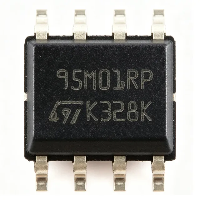
M95M01-RMN6TP - 1Mbit SPI EEPROM | STMicroelectronics
M95M01-RMN6TP

M95M01-RMN6TP - 1Mbit SPI EEPROM | STMicroelectronics

The M95M01-RMN6TP is a 1-Mbit (128 Kbyte) serial EEPROM from STMicroelectronics, organized as 131,072 x 8 bits and accessed via a high-speed SPI bus. It operates from a single 2.5V to 5.5V power supply, supports clock frequencies up to 16 MHz, and is housed in a standard 8-pin SOIC (SO-8N) package. Data verified as of 2026-08-05. An EEPROM (Electrically Erasable Programmable Read-Only Memory) is a non-volatile memory that retains data when power is removed and can be electrically erased and reprogrammed in-system. It sits within the memory hierarchy as a type of non-volatile memory, below flash memory in density but offering byte-level erase/write granularity and higher endurance for frequent small updates. In the product taxonomy, EEPROM is a subclass of memory ICs, which fall under integrated circuits, ultimately part of the broader semiconductor category. Key features include a 16 MHz SPI interface (SPI-compatible modes 0 and 0), a write time of 5 ms typical, and a write endurance of 4 million write cycles per byte. The device also offers a 200-year data retention at 55°C, a page size of 256 bytes, and a self-timed programming cycle with automatic address increment. The SO-8N package is widely used and footprint-compatible with many industry-standard EEPROMs, enabling drop-in replacement in existing designs. The M95M01 uses a standard SPI protocol with Chip Select (S), Serial Clock (C), Serial Data Input (D), and Serial Data Output (Q) pins. It includes a Write Protect (W) pin and a Hold (HOLD) pin for suspending communication without resetting the device. The memory array is organized into pages, and the device supports sequential read and write operations across page boundaries, simplifying firmware design. Typical applications include industrial automation parameter storage, smart metering data logging, medical device calibration data, and automotive electronics (non-safety-critical) where reliable non-volatile storage is required. The wide voltage range and high endurance make it suitable for frequent data updates in embedded systems. When designing with this device, ensure the SPI bus is properly terminated and that the Write Protect pin is controlled to prevent accidental writes. The HOLD pin should be pulled high if unused. For high-reliability applications, consider the device's 4 million write cycle endurance and 200-year data retention specifications. This page synthesizes distributor pricing, drop-in alternatives, and practical design notes not found in the STMicroelectronics datasheet, providing engineers with a comprehensive resource for selecting and using the M95M01-RMN6TP.

USD $1.05 お問い合わせ
M95M02-DRMN6TP - 2Mbit SPI EEPROM | STMicroelectronics
M95M02-DRMN6TP

M95M02-DRMN6TP - 2Mbit SPI EEPROM | STMicroelectronics

The M95M02-DRMN6TP is a 2-Mbit (256 Kbyte) serial EEPROM from STMicroelectronics, organized as 262,144 x 8 bits and accessed via a high-speed SPI bus. It operates from a 1.8V to 5.5V supply, supports clock frequencies up to 20 MHz, and is housed in a compact SO-8N package. This device is designed for applications requiring reliable, non-volatile data storage with low power consumption and high endurance. An EEPROM (Electrically Erasable Programmable Read-Only Memory) is a type of non-volatile memory that can be electrically erased and reprogrammed. It retains data without power, making it essential for storing configuration parameters, calibration data, and small amounts of firmware in embedded systems. EEPROMs are part of the broader memory IC hierarchy: EEPROM -> serial EEPROM -> SPI EEPROM -> non-volatile memory -> semiconductor memory. The SPI interface provides a simple, high-speed serial connection using just four wires (SCK, MOSI, MISO, CS), reducing pin count and PCB area compared to parallel EEPROMs. Key features of the M95M02-DRMN6TP include a 20 MHz maximum clock frequency, byte and page write modes (up to 256 bytes per page), and a write time of 5 ms per page. It offers a write endurance of 4 million write cycles and data retention of 100 years, ensuring long-term reliability. The device also includes a hardware write-protect pin (WC) and a status register with a Write-In-Progress (WIP) bit for software polling. The SO-8N package is industry-standard, enabling drop-in compatibility with many other 2-Mbit SPI EEPROMs. Technically, the M95M02-DRMN6TP uses a floating-gate transistor architecture, which is standard for EEPROM technology. The SPI interface supports modes 0 and 3, and the device is compatible with both 3-wire and 4-wire SPI configurations. The memory array is organized into 1024 pages of 256 bytes each, allowing efficient block writes. The device also features a deep power-down mode that reduces current consumption to 1 uA, ideal for battery-powered applications. Typical applications include industrial automation for storing calibration and configuration data, smart meters for logging consumption data, and automotive electronics for storing VIN and diagnostic information. The wide voltage range and high endurance make it suitable for harsh environments. In IoT devices, it stores device credentials and sensor calibration data. When designing with this device, ensure the SPI bus is properly terminated and the CS pin is held high when the device is not selected. Use a 0.1 uF decoupling capacitor close to the VCC pin. For write operations, poll the WIP bit or wait 5 ms before initiating the next command to avoid data corruption.

見積もり お問い合わせ
MA5302MSXUMA1 - 2-Ch Class D 440W Audio Amp | Infineon
MA5302MSXUMA1

MA5302MSXUMA1 - 2-Ch Class D 440W Audio Amp | Infineon

The Infineon MA5302MSXUMA1 is a 2-channel (stereo) Class D audio amplifier integrated circuit housed in a PG-IQFN-42-1 package, integrating a PWM controller, a high-voltage gate driver, and four low-RDS(ON) power MOSFETs in a multi-chip module (MCM). It delivers up to 440 W of output power and reaches 94% efficiency, supporting 1-2 ohm speaker loads for high-power subwoofer and professional audio systems. The MA5302MS family achieves power density equal to or greater than monolithic alternatives while occupying 50% less PCB space and requiring little or no external heatsink, making it ideal for space-constrained, thermally limited designs. A Class D audio amplifier is a switching amplifier topology that uses pulse-width modulation (PWM) to drive the output stage at high frequency, then low-pass-filters the resulting waveform to recover the audio signal. Compared with linear (Class A/AB) amplifiers, Class D designs achieve far higher efficiency (typically 85-95%) because the output transistors switch between fully on and fully off states instead of operating in their linear region. The MA5302MS belongs to the power amplifier -> audio amplifier -> Class D amplifier -> integrated Class D IC hierarchy within Infineon's MERUS multi-chip-module product line. Key specifications include 440 W maximum output power, 94% efficiency, 2-channel stereo or mono-BTL configuration, 1-2 ohm load support, integrated protection features, and a compact 7x7 mm PG-IQFN-42-1 package. The integrated gate driver and MOSFETs eliminate the need for an external half-bridge, reducing BOM cost and design complexity. The device is the successor to the IR43x2M family and shares the established MERUS audio platform footprint. The MA5302MS uses a multi-chip-module (MCM) architecture combining a 2-channel PWM controller, gate driver, and four power MOSFETs on a single substrate. This topology allows higher output power than monolithic CMOS Class D amplifiers because the discrete MOSFETs can be optimized for low RDS(ON) without competing for silicon area with the control logic. The result is higher continuous output current, lower thermal resistance, and the ability to drive very low-impedance (1-2 ohm) speaker loads that would otherwise require large external heatsinks. Typical applications include powered subwoofers, home theater systems, professional PA speakers, soundbars, marine audio systems, and automotive aftermarket amplifiers. The wide load range (1-2 ohm) makes it particularly suitable for subwoofer designs where low-impedance voice coils are common and high continuous power is required. When designing with this device, follow the Infineon reference design for board layout, output filter selection, and thermal management. The integrated protection suite includes thermal shutdown, overcurrent, and undervoltage lockout, but the PCB copper pour and thermal via pattern must still support continuous high-power operation. This page synthesizes distributor pricing, drop-in alternatives, and practical design notes not found in the manufacturer datasheet alone.

見積もり お問い合わせ
MA5342MSXUMA1 - 2x200W Class D Audio Amplifier MCM | Infineon
MA5342MSXUMA1

MA5342MSXUMA1 - 2x200W Class D Audio Amplifier MCM | Infineon

The Infineon MA5342MSXUMA1 is a 2x200W stereo Class D audio amplifier multi-chip module (MCM) integrating a 2-channel PWM controller, a high-voltage gate driver, and four low-RDS(ON) MOSFETs in a 7x7 mm PG-IQFN-42-1 package. It delivers equivalent or higher output power than monolithic alternatives while occupying 50% less board space and requiring little or no heatsink, achieving up to 95% efficiency. A Class D audio amplifier is a switching amplifier topology that uses pulse-width modulation (PWM) to drive the output stage at high frequency, then low-pass filters the resulting square wave to recover the audio signal. Compared to Class AB linear amplifiers, Class D amplifiers achieve significantly higher efficiency (typically 85-95% versus 50-70%), reducing power dissipation and enabling smaller form factors. The MA5342MSXUMA1 belongs to the amplifier IC family -> audio amplifier -> Class D amplifier -> power management IC taxonomy used by audio system designers. Key features include 2x200W continuous output power into 4 ohm loads, an integrated 49.2 mOhm RDS(ON) output stage, analog input interface, and support for supply voltages across the PG-IQFN-42-1 high-power split-rail topology. The device is footprint-compatible with the predecessor IR43x2M family, enabling drop-in upgrades in existing designs without PCB rework. Operating modes support both single-ended and bridge-tied load (BTL) configurations, covering home theater, soundbar, and subwoofer applications. The MA5342MSXUMA1 uses Infineon's proprietary MCM packaging that mounts the controller die, gate driver die, and four power MOSFET dice in a single leadless package. This reduces parasitic inductance between the gate driver and MOSFET gates, improving switching performance and EMI characteristics. The exposed thermal pad enables direct PCB heat spreading, allowing the part to deliver full-rated power without an external heatsink in typical 4 ohm applications. Typical applications include home theater receivers, powered stereo speakers, soundbars, subwoofers, automotive infotainment amplifiers, and professional powered monitors. The high efficiency and compact footprint make it well suited for slim-form-factor audio products where thermal management is constrained. When designing with the MA5342MSXUMA1, follow the reference design's LC output filter values to maintain loop stability and meet EMI targets. The exposed pad must be soldered to a sufficiently large copper pour for thermal dissipation - failure to do so can cause thermal shutdown at high output levels. This page synthesizes distributor pricing, drop-in alternatives, and practical design notes not found in the manufacturer datasheet.

見積もり お問い合わせ
MAC7111MAG40 - 32-Bit ARM7 MCU 512KB Flash 144-LQFP | NXP
MAC7111MAG40

MAC7111MAG40 - 32-Bit ARM7 MCU 512KB Flash 144-LQFP | NXP

The NXP MAC7111MAG40 is a 32-bit ARM7TDMI-S Flash microcontroller developed for embedded automotive body and chassis applications, delivering 50 MHz CPU performance with 512KB on-chip Flash and 144-LQFP (20x20 mm) packaging. It integrates a 16-channel 10-bit ADC, CAN 2.0 interface, enhanced I/O capability with external bus, and AEC-Q100 automotive qualification. Background: A 32-bit microcontroller (MCU) is a single-chip computer that integrates a processor core, program memory (Flash/ROM), data memory (RAM), and a rich peripheral set. The ARM7TDMI-S core is a 32-bit RISC architecture featuring the Thumb instruction set for improved code density, widely adopted in automotive and industrial embedded systems. Within the broader taxonomy, the MAC7111MAG40 belongs to the MCU -> microcontroller -> embedded processor -> semiconductor IC hierarchy, and to the Flash-based automotive MCU sub-family. Key features include 512KB program Flash, 32KB SRAM, 50 MHz core clock, 112 GPIO lines, 16-channel 10-bit ADC, two CAN 2.0A/B controllers, an external bus interface for memory expansion, and AEC-Q100 Grade 1 qualification supporting -40C to +125C operation. The MAC7111 family is pin-compatible with MAC7120/MAC7130/MAC7140 devices, allowing scalability between Flash sizes and peripheral mixes. Architecture depth: the MAC7111MAG40 uses the ARM7TDMI-S core with a 3-stage pipeline and Von Neumann bus. Its embedded Flash controller accelerates in-application programming, and the Enhanced Capture Timer (ECT) module supports up to 10 channels for precise PWM and pulse measurement. The device integrates a 16-channel 10-bit ADC with 7 us minimum conversion time. Typical applications include automotive body control modules (BCMs), instrument clusters, HVAC controllers, lighting modules, and CAN node ECUs. AEC-Q100 Grade 1 qualification makes it suitable for under-hood and chassis systems exposed to high thermal stress. Design consideration: when migrating from the MAC7110 to MAC7111 family, verify the external bus timing parameters against any SRAM or peripheral glue logic, and ensure that the 144-LQFP pad layout and pinout match the MAC71xx pin-compatible devices to enable drop-in scalability. This page consolidates distributor pricing, pin-compatible drop-in alternatives, and design notes that go beyond the manufacturer datasheet, supporting both new designs and lifecycle refresh decisions for long-life automotive programs.

見積もり お問い合わせ