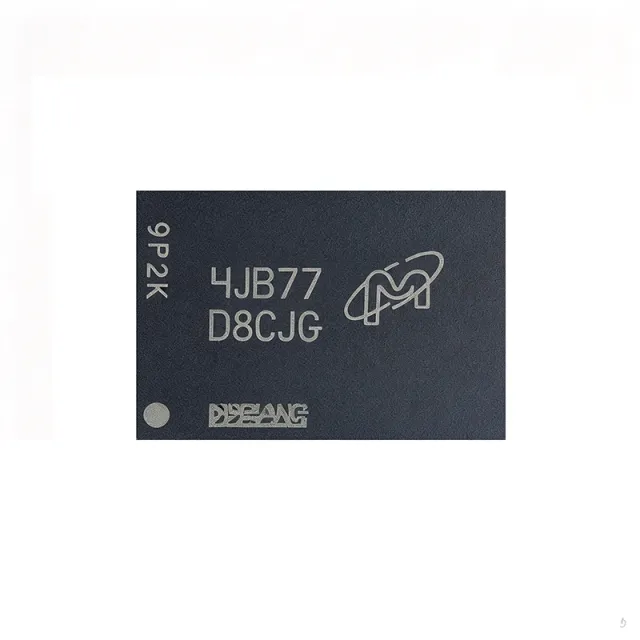
MT48LC4M32B2B5-7G
MT48LC4M32B2B5-7G - 128Mb x32 SDRAM 143MHz | Micron
The Micron MT48LC4M32B2B5-7G is a 128 Megabit (4M x 32-bit) Synchronous DRAM (SDRAM) organized as four internal banks, operating from a 3.0 V to 3.6 V single supply and packaged in a 90-ball 8 mm x 13 mm VFBGA (Tape and Reel). It delivers a 143 MHz maximum clock rate with a 5.5 ns access time and uses a fully synchronous interface with LVTTL-compatible I/O, an internal pipelined architecture, and programmable CAS latency of 2 or 3 clocks.
What is SDRAM? Synchronous DRAM is a generation of dynamic random-access memory that synchronizes all address, data, and control signals to a free-running system clock, in contrast to the asynchronous DRAM used in earlier PCs. Within the memory hierarchy, SDRAM sits above asynchronous DRAM and below Double Data Rate SDRAM (DDR), and within modern computing platforms it remains a low-cost, low-power solution for embedded graphics, networking line cards, set-top boxes, and industrial HMI where x32 bus width is convenient and DDR is unnecessary. SDRAM -> DRAM -> volatile memory -> semiconductor IC is the standard taxonomy.
Key features of the MT48LC4M32B2B5-7G include auto-refresh (64 ms / 4096 rows), self-refresh mode, four-bank operation with concurrent bank precharge, and a programmable burst length of 1, 2, 4, 8, or full page with sequential or interleave burst type. The device supports LVTTL levels on all inputs and outputs, has a deep power-down mode, and provides a CKE pin for clock enable/disable and clock suspend operation, enabling fine-grained power management in battery-backed or intermittently active systems.
Architecturally the part uses an internal pipelined 2n-prefetch architecture that allows the column address to change on every clock cycle, enabling fully random access. The four-bank design lets one bank be precharged while another is being accessed, which hides precharge cycles and sustains high throughput. The x32 organization maps directly to common 32-bit embedded buses such as 32-bit microcontrollers and DSPs, eliminating bus-width glue logic in many designs.
Typical applications include graphics buffers in laser printers and POS terminals, frame stores in industrial cameras, SDRAM expansion for 32-bit microcontrollers (PIC32MZ, STM32, NXP i.MX external memory bus), networking line cards and DSLAM buffers, and main memory for low-cost FPGA soft-core processors such as Nios II and MicroBlaze. The wide x32 data bus makes the part especially attractive where the host is already 32 bits wide.
When designing with the MT48LC4M32B2B5-7G, follow Micron TN-48-05 layout guidelines - matched-length clock, address, and command traces, a clean 3.3 V analog supply with local decoupling, Vss/VddQ noise isolation, and proper SSTL-style termination if multiple loads are present. Note that the -7G speed grade is the 143 MHz / CL3 commercial variant; the -7 IT:G variant is the industrial-temperature equivalent for -40 C to +85 C operation, and the -6A variant is the slower 166 MHz pin-compatible grade.
This page synthesizes distributor pricing, drop-in speed-grade alternatives within the same Micron x32 SDRAM family, and practical PCB design notes not found in the manufacturer datasheet.
見積もり
お問い合わせ