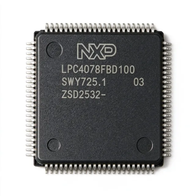
LPC4330FET256
LPC4330FET256 - Dual-core Cortex-M4/M0 MCU, 264KB SRAM | NXP
The NXP Semiconductors LPC4330FET256 is a dual-core ARM Cortex-M4/M0+ microcontroller with 264 KB SRAM, two High-Speed USB 2.0 ports with on-chip PHY, 10/100 Ethernet MAC, CAN 2.0, AES engine, SPIFI, SGPIO, and SCT timer/PWM subsystem, housed in a 256-ball LBGA (17x17 mm) package. It operates from a 2.2 V to 3.6 V supply, runs the M4 core up to 204 MHz and the M0 coprocessor up to 204 MHz, and integrates 83 GPIOs supporting multiple serial, parallel, and analog interfaces.
What is a microcontroller? A microcontroller (MCU) is a single-chip computer that integrates a CPU core, memory (SRAM and non-volatile storage), and programmable I/O peripherals. The LPC4300 series is positioned as a high-performance digital signal controller class MCU, combining deterministic real-time DSP from the Cortex-M4 with the low-latency I/O handling of a Cortex-M0 coprocessor — a hypernym hierarchy of MCU -> embedded processor -> semiconductor. The 'flashless' designation means the LPC4330 has no on-chip flash; code is executed from external QSPI flash via SPIFI or from internal SRAM, which simplifies the silicon for high-reliability designs and supports secure-boot applications.
Key features include dual-core asymmetric multiprocessing (Cortex-M4 with FPU + Cortex-M0), 264 KB total SRAM, two Hi-Speed USB 2.0 ports with integrated PHY, 10/100 Ethernet MAC, CAN 2.0B, AES-128 hardware accelerator, SPI Flash Interface (SPIFI) for external code storage, Smart GPIO (SGPIO), State Configurable Timer (SCT), LCD controller supporting up to 1024 x 768, 12-bit ADC, 10-bit DAC, and a Smart Card interface. The LBGA256 package is rated for -40 C to +85 C operation.
Technical depth: the Cortex-M4 includes a single-precision IEEE 754 floating-point unit and DSP extensions (SIMD, MAC), enabling audio, motor-control, and signal-processing workloads; the Cortex-M0 offloads real-time I/O servicing so the M4 core is never blocked. Memory architecture: 264 KB SRAM is split between system RAM and peripheral buffers; SPIFI provides XIP (execute-in-place) from Quad-SPI flash at up to 40 MB/s, eliminating the need for parallel memory bus. The HS-USB PHY embeds the 1.5 kOhm pull-up and current-mode termination so only external capacitors are required on D+/D-.
Typical applications include industrial control HMI with TFT LCD, multi-axis motor control, audio processing, USB peripherals and hubs, Ethernet-connected IoT gateways, secure payment terminals, point-of-sale systems, robotics, and dual-core asymmetric processing designs where the M0 handles comms and the M4 runs control loops. The wide peripheral set also suits smart-meter, medical instrumentation, and printer/scanner controllers.
Design consideration: because the part is flashless, every board must boot from an external SPIFI flash, ISP-mode UART, or USB DFU. Validate SPIFI timing at your M4 clock; the SPIFI controller must be reconfigured for each flash JEDEC ID. The LBGA256 requires a 0.8 mm ball pitch and PCB microvia/stacked-via process for fan-out.
This page synthesizes distributor pricing, drop-in alternatives within the same LBGA256 footprint, and practical design notes not found on a single manufacturer datasheet page.
見積もり
お問い合わせ