電源管理
サブカテゴリ
製品 (2819)

BCM6123TD1E5126T0R - 6123 ChiP Bus Converter Module | Vicor
The Vicor BCM6123TD1E5126T0R is an isolated, through-hole ChiP (Converter housed in Package) BCM Bus Converter Module that steps a nominal 380V high-voltage DC input down to a 47.5V SELV output with 25.7A continuous secondary current capability. Housed in the 6123 ChiP through-hole package (63.34 mm x 22.80 mm x 7.21 mm), it delivers up to 1876 W/in3 power density with 97.9% peak efficiency, and provides 4,242 VDC isolation between input and output. A BCM (Bus Converter Module) is a fixed-ratio, isolated DC-DC converter used as a building block inside Vicor's Factorized Power Architecture (FPA). It typically operates as a K=1/8 transformer in the BCM6123 family, stepping a high-voltage primary distribution bus (here 260-410 VDC) down to a Safety Extra Low Voltage (SELV) secondary bus (8.1-51.3 V) feeding downstream PoL regulators. Within the broader taxonomy it sits as: power module -> DC-DC converter -> isolated bus converter -> Vicor ChiP platform. Key differentiating specifications include the analog (telemetry/control) interface revision, full 25.7 A continuous output with no derating across the input range, OV/OC/UV protection plus short-circuit and thermal protection, and parallel operation support for multi-kilowatt arrays. The 6123 ChiP platform also enables bidirectional current flow between HVDC bus and SELV bus when paired with a Vicor AC rectifier or downstream regulator. The 6123 ChiP BCM uses Vicor's proprietary ZVS (Zero-Voltage Switching) and ZCS sine amplitude converter topology, allowing fixed-ratio conversion at megahertz switching frequencies with very low switching loss. The 4,242 VDC galvanic isolation supports 380V distribution in telecom central offices, data center 400V racks, and industrial DC microgrids where personnel safety on a SELV secondary matters. Typical applications include 48V telecom bus distribution from a 380V HVDC bus, data center 400V-to-50V intermediate bus conversion feeding PoL regulators, and renewable-energy battery storage interfaces requiring bidirectional capability. The BCM6123 is also used in industrial HVDC motor drive DC-links where galvanic isolation and high power density minimize cabinet footprint. Designers should observe Vicor's PCB layout guidance: the through-hole ChiP requires a matched land pattern, thermal vias under the package base, and LC input filtering tuned to the 380V bus to manage reflected ripple. Always parallel BCM modules using Vicor's recommended droop-sharing scheme rather than connecting outputs directly without current sharing. This page synthesizes distributor pricing, parametric alternatives, and practical design notes not found in the manufacturer datasheet alone.
BCR320UE6327HTSA1 - 250mA Linear LED Driver, 27V, SC-74-6 | Infineon
The Infineon BCR320UE6327HTSA1 is a 250 mA linear constant-current LED driver IC housed in a 6-pin PG-SC74 (SOT-26 equivalent) surface-mount package, designed to drive low- and mid-power LEDs in general lighting and automotive applications. It accepts a wide 1.4 V to 27 V supply input and regulates a fixed output current of approximately 250 mA, eliminating the need for an external current-setting resistor while keeping the BOM extremely small. A linear LED driver is a semiconductor device placed in series with the LED string that absorbs the excess voltage between the supply rail and the LED forward voltage, holding current constant through a built-in reference and sense transistor. Within the broader product hierarchy, the BCR320U belongs to the linear LED driver class, which sits under LED drivers, then power management ICs, then semiconductor ICs. By operating in the linear region rather than switching, the BCR320U introduces zero switching ripple onto the LED current, producing visually flicker-free output - critical for interior lighting, dashboard backlights, and indicator lamps where stroboscopic effects are unacceptable. Key specifications include 250 mA nominal output current, a 1.4 V to 27 V input range, integrated reverse-polarity protection, and a typical negative temperature coefficient of -0.2 %/K that progressively reduces output current as junction temperature rises - a built-in thermal foldback that protects both the driver and the LED from thermal runaway. The integrated reverse-polarity MOSFET eliminates a discrete protection component, shrinking the footprint for space-constrained PCB designs. Architecturally, the BCR320U combines an internal bandgap reference, a sense resistor, and a pass transistor monolithically, so the only external components required are the supply bypass capacitor and the LEDs themselves. The device is qualified to AEC-Q101, allowing deployment under the hood and in other harsh automotive electrical environments. Typical applications include automotive interior lighting such as dome lights and reading lamps, instrument cluster backlighting, status and indicator LEDs in white goods, signage and channel-letter illumination, and low-power architectural accent lighting. Compared to a discrete resistor biasing scheme, the BCR320U delivers uniform brightness across multiple LEDs regardless of forward-voltage variation and significantly extends LED lifetime by limiting inrush and thermal stress. When designing with this part, ensure adequate copper area beneath the exposed pad to keep the junction temperature within the -40 C to +150 C operating range. Place the input bypass capacitor as close as possible to the VCC pin to suppress voltage transients on long automotive wiring harnesses, and observe the maximum input voltage of 27 V including load-dump excursions. This page combines distributor pricing tiers, AEC-Q101-grade drop-in alternatives, and practical PCB layout notes that go beyond the manufacturer datasheet to help engineers select and source the BCR320U for next-generation LED lighting designs.

BCR420UE6327 - 200mA Linear LED Driver, 40V, PG-SC74-6
The Infineon BCR420UE6327 is a 200 mA linear constant-current LED driver IC housed in a 6-pin PG-SC74-6 (SOT-23 equivalent) surface-mount package. It regulates LED current through an external resistor on the RE pin and is rated for supply voltages of 40 V and above, suiting it to 12 V and 24 V automotive and industrial rails. The device integrates a low-side NPN driver transistor plus control circuitry, so only a single resistor and decoupling capacitor are needed for a complete LED string driver. A linear LED driver is a constant-current regulator that absorbs the voltage difference between the supply rail and the LED string, holding forward current stable across LED binning, temperature drift, and supply variation. Linear LED drivers belong to the broader category of constant-current regulators, which themselves are a subset of power-management ICs and analog signal-chain semiconductors. Compared to switching LED drivers, linear drivers add no EMI, no switching ripple, and no inductors, but dissipate the excess voltage as heat on the die. Key features of the BCR420UE6327 include continuous output current up to 150 mA when using a single external resistor (up to 200 mA per the manufacturer's product page), a 40 V supply rating, a micro-controller-compatible PWM input, and an internal negative temperature coefficient of about -0.2 %/K that thermally protects the LEDs and the IC without external thermistors. The PG-SC74-6 footprint is JEDEC-standard and supports reflow soldering on standard lead-free profiles. Architecturally, the part uses a precision bandgap-derived reference and a low-side NPN pass transistor in a feedback loop that senses current through the external resistor. Because the current setting is analog and resistor-programmed, no firmware or digital interface is required. The driver therefore drops into simple stand-alone LED circuits as well as micro-controlled dimming arrangements where the digital enable pin is driven by a GPIO. Typical applications include automotive interior and exterior lighting (dome, ambient, side-marker, and tail lamps), industrial signage and status indicators, architectural strip lighting, and white-goods display backlights. The wide voltage headroom also makes it a useful tail-light driver on 24 V commercial-vehicle buses. When designing with the BCR420UE6327, choose the RE resistor using I_LED = V_RE / R_RE, derate the dissipation budget for the worst-case VIN - V_LED drop, and respect the thermal resistance of the PG-SC74-6 land pattern. This page consolidates distributor pricing, drop-in alternatives, and practical design notes that go beyond the manufacturer datasheet.

BCR431UXTSA1 - 36.5mA Linear LED Driver, 42V | Infineon
The Infineon BCR431UXTSA1 is a 36.5 mA constant-current linear LED driver housed in a 6-pin PG-SOT23-6 surface-mount package. It integrates a single-channel linear regulator with internal current setting, eliminating the need for an external current-sense resistor, and supports supply voltages up to 42 V at the input. The fixed 36.5 mA output is trimmed at the Infineon factory, providing tight tolerance without external calibration. A linear LED driver (also called an LED current regulator or constant-current sink) is a type of power management IC that delivers a regulated current to a string of one or more LEDs. Linear drivers sit within the broader hierarchy of power management semiconductors: linear LED driver -> constant-current regulator -> LED driver -> power management IC. They are preferred over switching LED drivers in applications requiring low EMI, small PCB area, and minimum BOM cost. Key features of the BCR431UXTSA1 include its 36.5 mA preset output current with ±10% tolerance across the full operating range, a wide 1.4 V to 42 V supply input range, low headroom voltage of typically 0.6 V, and integrated reverse-polarity protection at the output. The SOT23-6 footprint occupies less than 9 mm² of board space, allowing placement close to the LED load. Architecturally, the BCR431UXTSA1 uses a high-side current-mirror reference and an integrated bipolar pass transistor to regulate the output current. This topology keeps the LED cathode referenced to ground, simplifying heatsinking and PCB layout. Because the device is a linear controller, thermal dissipation equals (VIN - VLED_STACK) x IOUT, so engineers must budget the SOT23-6 31 C/W θJA accordingly. Typical applications include small LED signs, channel-letter illumination, architectural cove lighting, and 24 V industrial signaling strips where EMI from switchers must be avoided. The 42 V input ceiling also suits 36 V industrial bus rails. When designing with the BCR431UXTSA1, ensure that the worst-case VIN - VLED total stays below the 42 V absolute maximum and that the SOT23-6 power dissipation does not exceed the thermal envelope. This page synthesizes distributor pricing, drop-in alternatives, and practical design notes not found in the manufacturer datasheet.
BD49E27G-MTR - 2.7V CMOS Voltage Detector, SSOP-5 | ROHM
The ROHM Semiconductor BD49E27G-MTR is a 2.7V CMOS-output voltage detector (voltage supervisor / reset IC) housed in a 5-pin SSOP package. It belongs to ROHM's BD49E series of standard CMOS voltage detectors designed for high-accuracy voltage monitoring with low quiescent current draw. The suffix -M denotes the automotive-grade part, and -TR denotes tape-and-reel packaging, making this MPN a fully automotive-qualified, surface-mount-ready variant. A voltage detector (also called a voltage supervisor or reset IC) is a type of power management IC that monitors a system supply rail and asserts a reset signal whenever the monitored voltage drops below a precise internal threshold. Voltage detectors sit below voltage regulators and supervisors in the power-management hierarchy, and above simple comparators because they integrate an accurate bandgap reference, hysteresis, and a defined output stage. The BD49E27G-MTR uses a CMOS push-pull (totem-pole) output stage rather than an open-drain output, which means it actively drives the output high or low without needing an external pull-up resistor. Key features include a 2.7V detection voltage with high accuracy (typically ±1% across the operating temperature range), very low quiescent current (in the single-digit microamp range), a CMOS output stage that can source and sink current, and built-in hysteresis to prevent chattering near the threshold. The 5-SSOP package provides a compact footprint suitable for space-constrained designs. Automotive-grade (-M) qualification means the device has been characterized for the extended temperature ranges and reliability demanded by vehicle electronics. Typical applications include microcontroller reset supervision in automotive ECUs, body and chassis control modules, infotainment system power-good indication, battery-pack monitoring, and any 3.3V or 5V logic rail that requires a deterministic reset signal at power-up, power-down, or brownout conditions. The 2.7V threshold is particularly suited to 3.3V rails that must be considered valid only after the rail has stabilized well above its minimum operating voltage. When designing with this part, place the bypass capacitor recommended in the datasheet as close as possible to the VCC pin to prevent false triggering from supply noise. The CMOS output eliminates the need for an external pull-up but the trace from the output to the microcontroller reset pin should be kept short to minimize EMI coupling. This page synthesizes distributor pricing, lifecycle status, drop-in alternatives, and practical design notes not found in the manufacturer datasheet.

BD50C0AFP-CE2 - 5V 1A 35V LDO Regulator, AEC-Q100 | ROHM
The ROHM Semiconductor BD50C0AFP-CE2 is a 1A high-accuracy, low-saturation positive-fixed LDO linear regulator delivering a fixed 5.0 V output from a TO-252-3 (DPAK) surface-mount package. It accepts a wide 6 V to 26.5 V input (with 35 V transient rating) and provides 1 A of continuous load current with built-in over-current protection and thermal shutdown for automotive-grade reliability. An LDO (Low-Dropout) linear regulator is a type of voltage regulator that maintains a stable output voltage even when the input voltage is very close to the output voltage. As a member of the linear regulator family within voltage regulators and the broader power management IC hierarchy, the BD50C0AFP-CE2 trades efficiency for simplicity: it dissipates (VIN - VOUT) x IOUT as heat rather than switching, which yields extremely low output noise - a benefit for analog and automotive sensor rails. Key features include a fixed 5.0 V output (no external resistor divider needed), 1 A continuous output current, internal over-current and thermal-shutdown protection circuits, and a low-saturation regulator topology that minimizes dropout loss. The TO-252-3 (DPAK) tab provides a low thermal resistance path, and the part is AEC-Q100 qualified, making it suitable for harsh automotive environments such as engine-control units and body electronics. The architecture uses a PNP/DMOS pass element with a precision bandgap reference and error amplifier, achieving tight line/load regulation while keeping quiescent current low. Because there is no switching node, EMI emissions are near-zero compared to a DC-DC converter, eliminating the need for shielding or complex LC filtering near sensitive analog or RF circuitry. Typical applications include automotive body-control modules, instrument-cluster power rails, sensor supplies (camera, radar, LiDAR peripherals), infotainment subsystems, and 24 V industrial bus regulation where a clean 5 V rail is needed. The AEC-Q100 qualification supports under-hood and chassis-mounted designs. When designing with this part, ensure adequate copper pour on the DPAK tab to keep junction temperature within safe limits. At VIN = 24 V and VOUT = 5 V at 1 A the regulator dissipates about 19 W, so derate IOUT or VIN significantly for continuous operation without a heatsink. This page synthesizes distributor pricing, drop-in alternatives, and practical design notes not found in the manufacturer datasheet alone.

BD7690FJ-E2 - 220kHz BCM PFC Controller | ROHM
The ROHM Semiconductor BD7690FJ-E2 is a 220 kHz boundary-conduction-mode power-factor-correction controller for AC/DC supplies, with a 10 V to 26 V supply range and an 8-SOP-J surface-mount package. It uses Zero Current Detection to reduce switching loss and noise. Its primary function is to shape the input current drawn from an AC source, improving input power factor for power supplies that require active PFC. A power-factor-correction controller is a specialized power-management IC used between an AC input and a DC power-conversion stage. The BD7690FJ-E2 controls the switching behavior of the PFC stage in boundary conduction mode, which supports high-frequency operation while helping reduce conduction-related loss and electromagnetic interference. Its 220 kHz switching frequency is a central design parameter for inductor selection, switching-device selection, and layout planning. Key verified features include boundary-conduction-mode operation, a 220 kHz switching frequency, a 10 V to 26 V supply range, 65 µA startup current, a -40 °C to +105 °C operating-temperature range, and an 8-SOP-J package. These figures make the device relevant to AC/DC power supplies, power-factor-correction stages, industrial power conversion, and other applications where input-current shaping and active PFC are required. The controller's Zero Current Detection function is intended to identify the switching-current zero-crossing condition and support reduced switching loss and noise. Designers should still validate the complete power stage against the datasheet, including gate-drive timing, current-sense limits, inductor ripple, startup behavior, protection settings, and the selected switching MOSFET. The supplied evidence confirms the package, operating class, voltage range, temperature range, and nominal switching frequency, but does not provide every electrical limit needed for a complete power-conversion design. Typical implementations place the controller in a boost-derived PFC stage that rectifies the AC input and raises the DC bus voltage while shaping line current. The same topology can support industrial power supplies and other AC/DC equipment requiring active power-factor correction. The compact 8-SOP-J package helps reduce board area, but high-frequency power conversion still requires careful layout around the high-current switch node, current-sense path, gate drive, and power ground. When selecting a replacement, verify the manufacturer pinout, switching frequency, supply range, control method, protection behavior, package dimensions, and thermal requirements rather than relying on the BC700 family name alone. This page synthesizes the supplied distributor and manufacturer references, available commercial data, application guidance, and design considerations for engineers evaluating the BD7690FJ-E2.
BD7691FJ-E2 - 220kHz BCM PFC Controller | ROHM
The ROHM Semiconductor BD7691FJ-E2 is a boundary-conduction-mode power-factor-correction controller IC for AC/DC supplies, switching at 220 kHz and supplied in an 8-pin SOP-J package. It corrects the input-current displacement factor used by products requiring power-factor improvement. Its Zero Current Detection approach senses inductance through resistance, reducing switching loss and noise without requiring an auxiliary winding. A power-factor-correction controller is an AC/DC power-management IC that shapes switch-mode input current toward the input voltage. In the broader hierarchy, it belongs to switch-mode power controllers, power-management ICs, and semiconductors. BD7691FJ-E2 is intended for the front end of an AC/DC supply, where the upstream stage establishes power factor before energy is transferred to a downstream converter. The principal verified features are 220 kHz switching, boundary-conduction mode, and resistance-based Zero Current Detection. BCM supports reduced switching loss and noise reduction according to the ROHM product material. The resistance-based detection method removes the auxiliary-winding requirement identified by ROHM, reducing circuit complexity compared with winding-based detection. The 8-SOP-J format supports conventional surface-mount PCB assembly. The controller does not itself rectify the mains input or switch the power stage; it controls an external power MOSFET and boost-stage rectifier. Its control function depends on sensing the inductor and feedback conditions through an externally designed circuit. Component values for the inductor, MOSFET, current-sense network, capacitors, and compensation network must therefore be selected from the manufacturer application information rather than inferred from the distributor listing. Typical applications are PFC front ends in AC/DC adapters, industrial power supplies, appliance power systems, and other switched-mode supplies whose input stage requires active power-factor correction. The controller is most relevant where a BCM implementation and resistance-based zero-current detection simplify the auxiliary circuit compared with winding-based solutions. Designers must validate mains-side creepage, clearance, isolation, surge protection, loop layout, and safety limits in the complete power supply; package-level data alone does not establish regulatory compliance. Confirm the exact pin functions and ratings from the manufacturer datasheet before layout because the supplied search results do not expose a complete verified pin table. Pricing and technical data in this record are limited to the provided web sources as of 2026-10-21.
BD7692FJ-E2 - BCM PFC Controller 410-580kHz | ROHM
The ROHM Semiconductor BD7692FJ-E2 is a power factor correction controller IC for AC/DC supplies, using boundary conduction mode (BCM) at 410 kHz, 450 kHz, or 580 kHz and housed in an 8-SOP-J surface-mount package. The verified distributor listing identifies it as a PFC IC, while the manufacturer describes Zero Current Detection (ZCD) for switching-loss reduction, noise reduction, and auxiliary-winding-free operation. A power factor correction controller is a specialized power-management IC that shapes input current in offline AC/DC equipment so the upstream power system draws less reactive current. In the broader hierarchy, a PFC controller sits between the mains input and the primary-side switching converter. Boundary conduction mode allows the power stage to transition between continuous and discontinuous inductor-current operation, reducing conduction loss at light load while retaining controlled switching behavior. The BD7692FJ is intended for products requiring power-factor improvement. Its three verified switching-frequency choices provide design flexibility when balancing transformer size, electromagnetic interference, switching loss, and output-ripple requirements. The manufacturer specifically highlights ZCD implemented through resistance detection, avoiding the need for an auxiliary winding in the power stage. This can simplify transformer construction and reduce the number of sensing connections when the sensing arrangement is implemented according to the datasheet. The BD7692FJ-E2 is supplied in an 8-SOP-J package. Its operating electrical limits, protection thresholds, control-loop details, current-sense range, startup behavior, and exact pin functions are not present in the supplied verification snippets; those values must be confirmed from the ROHM datasheet before layout or production release. The product is therefore best treated as a controller for a carefully validated primary-side PFC stage rather than as a complete power converter. Typical applications include AC/DC power supplies, industrial power systems, and equipment with upstream universal-input requirements where active PFC is needed. In a practical design, the controller drives an external boost switch and receives current or voltage information from the power stage. The verified 410 kHz, 450 kHz, and 580 kHz options should be selected according to the magnetics design and EMI constraints. The key design consideration is validating the complete feedback and protection network rather than relying only on the controller MPN. Check the ROHM application guidance, confirm the current-sense and ZCD implementation, and verify startup, overcurrent, open-loop, and thermal behavior against the manufacturer limits. This page combines verified source links, application context, and engineering selection guidance while leaving unsupported numeric claims explicitly marked as data needed.
BD8LA700EFV-CE2 - 8-Ch Auto Low-Side Switch, 24-HTSSOP-B | ROHM
The ROHM BD8LA700EFV-CE2 is an automotive-grade 8-channel low-side switch in a 24-pin HTSSOP-B package, integrating eight N-channel power MOSFETs with a CMOS control block on a single monolithic silicon die. Each channel delivers up to 200 mA continuous drain current, while built-in open-load detection, over-current protection, active clamping, and thermal-shutdown circuits safeguard the device and downstream wiring in harsh electrical environments. The -CE2 suffix indicates the part is qualified to automotive reliability standards and ships on tape-and-reel for high-volume assembly. A low-side switch is a power-distribution topology in which the load (lamp, solenoid, relay coil, LED string) is tied to V_BAT, and the MOSFET is placed between the load and ground. Pulling the MOSFET gate high by the MCU sinks current to ground and energizes the load; releasing the gate de-energizes it. Compared with high-side switches, low-side drivers simplify diagnostic feedback because the load-end is always at battery potential, enabling robust open-load detection even when the switch is off. Key features include 3 V to 5.5 V logic supply, integrated flyback/active clamp for inductive loads, parallel-channel operation for higher currents, very low quiescent current in standby, and built-in diagnostic flags (open-load, short-to-ground, over-temperature). The HTSSOP-B exposed pad lowers thermal resistance so all eight channels can run at full duty in ECU and BCM modules. Typical applications include automotive body-control modules (BCM) driving lamps and indicators, junction-box load drivers, HVAC actuator switching, and rear-lamp clusters. ROHM PCB OEMs' monolithic CMOS-plus-power-MOS architecture integrates the MOSFET and CMOS control on 1 chip, reducing PCB area versus discrete MOSFET arrays and improving fault-coverage uniformity across channels. When designing with this device, ensure the supply decoupling, exposed-pad soldering, and ground-return layout follow the manufacturer's reference pattern. The CE2 part is shipped over six distributors; pricing varies by reel size. This page synthesizes distributor pricing, drop-in alternatives, and practical design notes not found in the manufacturer datasheet.

BD9B304QWZ-E2 - 3A Sync Buck DC/DC, 2.7-5.5V Input | ROHM
The ROHM BD9B304QWZ-E2 is a synchronous step-down (buck) DC/DC converter IC with built-in low on-resistance power MOSFETs, housed in an 8-pin XFDFN exposed-pad (UMMP008AZ) package. It accepts an input voltage range of 2.7V to 5.5V and delivers up to 3.0A continuous output current with an adjustable output voltage from 0.8V up to 0.8 x VIN, set by an external resistor divider. A buck (step-down) DC/DC converter is a switch-mode power supply topology that efficiently converts a higher DC input voltage to a lower DC output voltage by rapidly switching an inductor-capacitor filter network. Buck converters sit within the broader hierarchy of voltage regulators -> DC-DC converters -> power management ICs -> semiconductors, and are preferred over linear regulators whenever (VIN - VOUT) x IOUT would create excessive heat dissipation. The synchronous topology replaces the traditional Schottky rectifier with a second MOSFET to reduce conduction loss. Key features include a 1.0 MHz / 2.0 MHz selectable switching frequency (set by an external resistor), built-in 40 mOhm high-side and low-side N-channel MOSFETs, constant on-time (COT) control for fast transient response, internal soft-start, and over-current / thermal shutdown protection. The selectable frequency allows the designer to trade efficiency against inductor size. The COT architecture produces a near-ripple-free output with a small output capacitor and eliminates the compensation network typical of voltage-mode or current-mode PWM parts. High-side and low-side RDSon of 40 mOhm each keep full-load efficiency in the mid-90% range at 5 V to 3.3 V conversion, and the 1 MHz / 2 MHz switching options push the fundamental above the AM band for EMI-sensitive consumer designs. Typical applications include point-of-load (POL) rails for FPGAs, ASICs, and SoCs, USB Type-C / PD auxiliary supplies, portable battery-powered devices running from a single-cell Li-ion (2.7V-4.2V) or 5V USB rail, solid-state drive (SSD) power management, and HDMI / DisplayPort interface power. The exposed thermal pad of the XFDFN-8 package ties directly to a small ground copper pour for heat extraction. When designing with the BD9B304QWZ-E2, pay attention to inductor selection - a 1.0 uH to 2.2 uH shielded power inductor is typical for 1 MHz operation. Keep the input/output ceramic capacitors (typically 22 uF X5R or X7R) within 2 mm of the IC pins to minimize parasitic loop inductance that could cause switching-node ringing. This page synthesizes distributor pricing, parametric drop-in alternatives in the same XFDFN-8 footprint, and practical design notes not found in the manufacturer datasheet alone.

BD9F500QUZ-E2 - 36V, 5A Synchronous Buck DC/DC Converter | ROHM
The ROHM Semiconductor BD9F500QUZ-E2 is a synchronous buck DC/DC converter with built-in low on-resistance power MOSFETs, rated for 4.5 V to 36 V input, 0.6 V to ~VIN adjustable output, and 5 A continuous load current, packaged in a 16-pin XFQFN (exposed pad). It uses ROHM's Nano Pulse Control™ constant-on-time (COT) architecture and integrates Light Load Mode for improved efficiency at low current. A buck (step-down) DC/DC converter is a switched-mode power supply topology that uses an inductor, output capacitor, and a control loop to reduce a higher DC input voltage to a lower regulated DC output voltage. ROHM's buck converters sit within the broader switching regulator family alongside boost, buck-boost, and SEPIC converters, all of which are sub-categories of switched-mode power conversion inside the power management IC hierarchy. Synchronous designs replace the external Schottky rectifier with a low-RDS(on) MOSFET to improve efficiency, especially at high load currents. The BD9F500QUZ-E2 features an adjustable output down to 0.6 V, integrated high-side and low-side MOSFETs, fast transient response from the COT control loop, Light Load Mode for light-load efficiency, and built-in protection functions such as over-current protection (OCP), under-voltage lockout (UVLO), thermal shutdown (TSD), and over-voltage protection (OVP). According to the manufacturer datasheet, the device operates from -40 °C to +85 °C (or +125 °C junction maximum) and is targeted at industrial, consumer, and 24 V bus distributed-power applications. The constant-on-time architecture delivers fast load-step response and a small external component count compared to traditional voltage-mode or current-mode PWM controllers. Combined with the 36 V maximum input rating, the BD9F500QUZ-E2 is positioned for industrial 24 V rails, factory automation, and distributed-power architectures where a compact, high-efficiency, 5 A point-of-load converter is required. Typical applications include 24 V industrial PLC power rails, SSD/NAS auxiliary supplies, FPGA core and I/O voltage rails, USB-PD source converters, and step-down conversion for 12 V automotive accessory subsystems. In multi-rail designs it can be paired with a higher-current master converter (e.g., a 8 A or 10 A ROHM BD9F800MUX-class part) plus an LDO for low-noise analog rails. When designing with this part, place the input ceramic bypass capacitor as close as possible to VIN and PGND, and use a low-impedance ground pour with sufficient thermal vias under the exposed pad to dissipate up to ~3 W of losses at full 5 A load. Ensure the inductor ripple current is within the data sheet's recommendation to avoid tripping OCP at the current-sense threshold during transient load steps. This page synthesizes distributor pricing, drop-in pin-compatible alternatives (same-brand first, then cross-brand), and practical PCB/thermal design notes that go beyond the manufacturer datasheet.

BM61M41RFV-CE2 - 3750Vrms Isolated Gate Driver, 65ns, 4A | ROHM
The ROHM BM61M41RFV-CE2 is a galvanically isolated single-channel gate driver with 3750 Vrms isolation voltage, 65 ns I/O delay time, and 4 A peak output current, housed in a 10-pin SSOP-BW package. The device uses magnetic coupling to deliver reinforced isolation between the input control logic and the high-voltage power stage, eliminating the need for an external gate-drive transformer or opto-coupler in many topologies. An isolated gate driver is a power-management IC that transmits a PWM or on/off control signal across a safety-grade isolation barrier while providing the high peak currents needed to rapidly charge and discharge the gate capacitance of a power MOSFET, IGBT, or SiC FET. Within the broader hierarchy, the BM61M41RFV-CE2 sits at: isolated gate driver -> gate driver -> power management IC -> semiconductor. Galvanic isolation is mandatory in motor drives, solar inverters, and industrial bus converters where the control side (ground-referenced, user-accessible) must remain safely separated from the high-voltage switching node referenced to a DC-link that may exceed 600 V or 1200 V. Key features include a minimum input pulse width of 60 ns (well below the pulse widths used in standard PWM schemes), an input-side supply range of 4.5 V to 5.5 V that interfaces directly to 5 V logic or 3.3 V microcontrollers through level shifting, and an output-side supply range of 9 V to 24 V supporting standard MOSFET (10-12 V), IGBT (15 V) and SiC (18-20 V) gate-drive requirements. The device provides a single driver channel and is rated for operation from -40 °C to +125 °C. Architecturally, the BM61M41RFV-CE2 integrates an on-chip micro-transformer that couples the input signal across the isolation barrier using high-frequency magnetic pulses, then reconstructs it on the secondary side to drive an output stage capable of sourcing and sinking the gate charge of mid-power switches. Compared with opto-coupler-based gate drivers, the magnetic-coupling approach avoids the slow propagation, LED-aging, and CTR-degradation issues that affect long-term reliability in high-temperature environments. Typical applications include driving low-side MOSFETs in half-bridge configurations (per the BM61M41RFV-EVK001/BM61M41RFV-EVK002 evaluation boards), IGBT gate drive in motor-control inverters, SiC FET drive in EV onboard chargers and DC-DC converters, isolated drive for solar micro-inverters, and digital isolator replacement where a small gate-driver coil offers PCB-area savings. When designing with this part, observe the input-side and output-side decoupling guidance from the ROHM datasheet - typically 1 µF to 10 µF low-ESR ceramics placed within 2 mm of each supply pin - and confirm that the bootstrap or isolated supply rail can deliver the peak 4 A during MOSFET Miller plateau transitions. For half-bridge or high-side drive, pair the BM61M41RFV-CE2 with a dedicated high-side/level-shift solution from the BM61 family such as the BM61S41RFV-CE2. This page synthesizes distributor pricing, drop-in alternatives within the BM61 family, and practical PCB layout notes not consolidated in the manufacturer datasheet alone.
BQ21061YFPR - 500mA 1-Cell Linear Charger 10nA Ship | TI
The Texas Instruments BQ21061YFPR is an I2C-controlled, 1-cell, 500-mA linear battery charger with 10-nA ship mode, integrated power-path with regulated PMID system voltage, and a low-dropout (LDO) post-regulator, all packaged in a 20-ball DSBGA (YFP) chip-scale package. The device charges single-cell Li-Ion or Li-Polymer batteries from a 3.9V to 6.45V input source and supplies a regulated 3.5V to 4.4V PMID output to the system load while simultaneously charging the battery. A battery charger IC is a specialized power management device that converts an external DC source (USB, wireless, solar, or adapter) into a precise current/voltage profile tailored to a battery's chemistry, while protecting the cell from over-voltage, over-current, and thermal stress. Linear chargers - as opposed to switching chargers - dissipate the excess VIN-VBAT voltage as heat, which makes them simpler, smaller, and noise-free, but limits their use to sub-1A applications where the thermal budget is acceptable. The BQ21061 sits at the high end of TI's nano-power charger family: 10-nA ship-mode quiescent current extends shelf life for years on primary cells, and the integrated PMID power-path allows the system to boot and run from the input source even with a deeply discharged or absent battery. Key features include programmable charge current up to 500 mA, ±0.5% battery regulation accuracy across -40°C to +85°C, dynamic power-path management (DPPM) that adjusts charge current to maintain PMID regulation, a programmable termination current down to 1 mA, and a thermal-regulation loop that automatically reduces charge current at high junction temperatures. The integrated 50-mA LDO can supply a clean rail to always-on peripherals (RTC, sensors, MCUs in sleep). The BQ21061 uses a switched-mode-style architecture on the charger section with a high-side P-channel FET pass element, a precision bandgap reference, and an 8-bit DAC for current/voltage programming over I2C. The PMID rail is regulated via a separate linear LDO controller and supports dynamic load sharing between input source, battery, and system load, ensuring no back-feed to the USB port. Typical applications include wearables (TWS earbuds, smartwatches, fitness bands), hearables, IoT sensor nodes, low-power medical patches, and any single-cell Li-Ion design that needs <100 nA quiescent current for multi-year storage. The wide VIN range (3.9V-6.45V) is fully compatible with USB, 5V adapters, and solar panels with MPPT front-ends. Design trade-off: because the charger is linear, total power dissipation = (VIN - VBAT) × ICHG. At 500 mA and VIN = 5V with a 4.2V battery, the device dissipates ~0.4W; designers must ensure the DSBGA thermal pad is soldered to a copper pour with thermal vias to avoid triggering the thermal-regulation loop unnecessarily. I2C address (default 0x6B) must be checked against any other charger on the same bus. This page synthesizes distributor pricing, drop-in alternatives from the BQ2106x family, and practical design notes not found in the manufacturer datasheet.
BQ21061YFPT - 500mA 1-Cell Linear Charger w/ 10nA Ship Mode | TI
The Texas Instruments BQ21061YFPT is a 500-mA I2C-controlled 1-cell linear battery charger with 10-nA ship mode, integrated power-path management, regulated system (PMID) voltage, and a built-in LDO, all integrated into a 20-ball DSBGA (YFP) package. It supports Li-Ion/Li-Polymer cells and provides a programmable charge current up to 500 mA with safety timers and thermal regulation, making it suitable for compact wearables, hearables, and IoT sensor nodes where PCB real-estate is severely constrained. The integrated power-path allows the system to operate directly from PMID while the charger simultaneously refuels the battery. A linear battery charger is a power management subcircuit which regulates charging current/voltage into a single-cell Li-Ion/Li-Polymer battery using a series pass element. Within the broader system taxonomy, a linear charger sits below a switching charger and below a power management IC, providing the safest and lowest-EMI charging path for small batteries at the cost of higher conduction dissipation. The BQ21061 specifically targets ultra-low-power IoT devices by combining charger + power-path + LDO in a single die, eliminating the need for a separate PMIC in simple wearable designs. Key features include a 10-nA ship mode quiescent current that dramatically extends shelf life on the warehouse shelf and during end-user storage, I2C programmability for charge current, input current limit, charger enable, and safety timers, integrated power-path with PMID regulation that allows system operation even with a deeply discharged or absent battery, and an integrated LDO that can supply low-voltage always-on rails for the host MCU. The 20-ball DSBGA package measures approximately 1.6 mm x 2.0 mm, enabling direct placement in space-constrained wearable form factors. The BQ21061 is engineered around a low-Rdson pass transistor architecture with an integrated sense resistor, providing high-accuracy charge current regulation and thermal management. Thermal regulation automatically reduces charge current at elevated die temperatures, protecting the device and battery in thermally constrained designs. The I2C interface allows host processors to dynamically adjust parameters and read status flags including charging state, fault conditions, and battery voltage. Typical applications include TWS earbuds charging cases, fitness bands, smart watches, IoT sensor nodes, Bluetooth trackers, and medical wearables such as continuous glucose monitors and pulse oximeters. Its combination of low quiescent current, small package, and integrated power-path makes it ideal for battery-powered products that must run for months on a single charge. When integrating this device, designers should follow TI reference layout guidance for the DSBGA thermal pad to ensure adequate heat dissipation during fast-charge at high VIN-VBAT differentials.
BQ24133QRGYRQ1 - 2.5A 1-3 Cell Buck Charger Q1 | TI
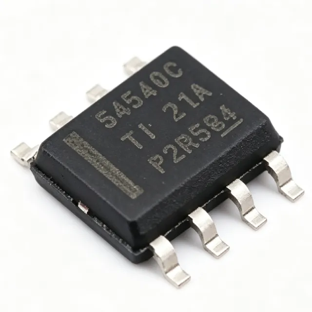
The Texas Instruments BQ24133QRGYR is an automotive-grade (AEC-Q100) stand-alone 1.6-MHz synchronous switched-mode Li-Ion and Li-Polymer battery charger with two integrated N-channel power MOSFETs, delivered in a 24-pin VQFN (RGY, 5.5x3.5 mm) package. It charges 1-cell, 2-cell, or 3-cell battery stacks at up to 2.5 A with a regulated 4.2 V/cell charge voltage. A switched-mode battery charger is a DC-DC converter-based power management IC that regulates charge current and battery voltage with far higher efficiency than linear chargers. Within the power-management IC hierarchy, the BQ24133 family sits between a generic buck regulator and a full battery management IC, adding charge termination, thermal regulation, and adapter-to-battery power path selection. Key features include a 1.6-MHz constant-frequency synchronous PWM controller delivering up to 92% efficiency, a 30-V input rating with adjustable input overvoltage protection, a 4.5-V to 17-V operating input range, and an automatic power path selector between the adapter and battery. High-accuracy regulation of input current, charge current, and charge voltage enables the device to safely work with limited-adapter-power systems, while dynamic power management protects overloaded sources. The device closely monitors battery pack temperature (TS pin with NTC) and permits charging only within a preset temperature window, an essential safety behavior for automotive and industrial lithium batteries. Integrated MOSFETs eliminate external discrete transistors, shrinking the solution footprint and reducing BOM count. Typical applications include automotive infotainment and telematics backup batteries, industrial handheld instruments, portable medical devices, and battery-backed servers or gateways requiring seamless adapter-to-battery transition. The power path feature keeps the system alive even with a deeply discharged battery. Design consideration: the 1.6-MHz switching frequency permits small inductors, but PCB layout of the power loop must be tight; place the inductor, input capacitor, and PGND connections per the datasheet layout guidelines to minimize EMI.

BQ24133RGYR - 2.5A 1.6MHz Sync Buck Charger | TI
The Texas Instruments BQ24133RGYR is a highly integrated stand-alone Li-Ion and Li-Polymer switched-mode battery charger with two integrated N-channel power MOSFETs. It operates as a 1.6-MHz synchronous buck charger delivering up to 2.5A charge current for 1-3 cell battery packs, housed in a 24-pin VQFN (RGY) package measuring 5.5x3.5 mm for space-constrained portable designs. A battery charger IC is a power-management device that safely controls charging current and voltage for rechargeable cells. The BQ24133 uses a synchronous buck converter topology to step down input voltage efficiently, minimizing heat compared to linear chargers. It belongs to the battery management IC hierarchy within power management semiconductors, essential for portable electronics, tools, and medical devices. Key features include high-accuracy regulation with plus/minus 1% charge voltage accuracy, a wide input range from a DC source as high as 17V including automotive car batteries, and an adjustable input overvoltage limit via the OVPSET pin with 30V rating on AVCC, ACP, and ACN pins. An integrated power path selector lets the system run from the adapter while charging the battery, and an external thermistor enables charging only within a safe temperature window. Technically, the constant-frequency synchronous PWM controller at 1.6 MHz permits small inductors and capacitors. Charge current is programmable via an external resistor, and cell count is configured for 1, 2, or 3 series cells. Thermal regulation reduces charge current when die temperature exceeds threshold, and a low-power sleep mode minimizes battery drain when input is removed. On high-voltage DC insertion, Q1 and Q2 remain off to protect the system. Typical applications include smartphones, tablets, digital cameras, power banks, solar-powered chargers, battery-powered industrial equipment, and medical devices. Design tip: ensure adequate copper pour for thermal dissipation and place input/output capacitors close to the IC; select the inductor based on the 1.6-MHz switching frequency to minimize ripple.
BQ24193 - I2C 4.5A Single-Cell USB/Adapter Charger | Texas Instruments
The Texas Instruments BQ24193 is an I2C-controlled, 4.5 A single-cell Li-Ion/Li-Polymer battery charger with narrow VDC power-path management and USB On-the-Go (OTG) boost operation, housed in a 24-pin 4 mm x 4 mm thin VQFN (RGE) package. The device integrates a switch-mode charger, input current and voltage regulation compliant with USB 2.0/USB 3.0 power specifications, system power-path management, and a synchronous boost converter that delivers 5 V on VBUS up to 1.3 A for OTG accessories. A switch-mode battery charger (SMBC) is a power management IC that converts an external supply (USB, adapter, or wireless) into a precisely regulated charging profile for a lithium-based cell while simultaneously managing the dynamic power path between the adapter, the system load, and the battery. Within the power-management hierarchy, it sits one level above simple linear chargers because its synchronous buck topology sustains high efficiency across wide VIN/VOUT ratios, reducing heat dissipation in space-constrained portable designs. Key features include a programmable charge current up to 4.5 A, ±0.5% battery regulation accuracy, 20 V tolerant input with overvoltage protection, configurable thermal regulation thresholds, and an I2C interface for charge-parameter programming, status telemetry, and interrupt reporting. The narrow-VDC topology keeps VBUS just above VBAT during system load transients, minimizing adapter current overshoot while extending adapter compatibility. Architecturally, the BQ24193 pairs a synchronous buck charger with a boost controller sharing the same power-stage pins, enabling seamless OTG reverse operation without external MOSFETs. Integrated input-current sensing, dynamic power-path management (DPPM), and JEITA temperature monitoring reduce external component count by typically 15-20 components versus discrete solutions, making the part well suited to compact tablet, ultrabook, and power-bank designs. Typical applications include single-cell Li-Ion tablets, ultrabook charging sub-systems, USB-PD/QC adapter charging, portable medical monitors, and OTG-capable power banks that supply 5 V to downstream accessories. Engineers commonly pair the BQ24193 with a USB Type-C PD controller on the input side and a Li-Ion gauge IC on the battery side. A key design consideration is thermal management: at VIN = 9 V, VBAT = 4.2 V, and ICHARGE = 3 A, the device dissipates an estimated 14 W. Designers should compute PCB copper area against the datasheet theta_JA value and add thermal vias under the exposed pad to keep Tj below 125 C. Charge-parameter defaults in non-volatile memory should be configured before production to prevent undefined behavior on first power. This page synthesizes distributor pricing, verified drop-in alternatives in the BQ2419x family, and practical design notes not consolidated in the manufacturer datasheet, helping engineers shorten their evaluation cycle.

BQ24195L - 2.5A USB Charger with 5.1V Boost | TI
The Texas Instruments BQ24195L is a 2.5 A single-cell USB and adapter battery charger with a 5.1 V, 1.0 A synchronous boost output, housed in a 24-pin 4.00 × 4.00 mm thin VQFN package. It integrates input-current and input-voltage regulation, battery charging, power-path management, and an I2C-controlled interface for portable power-bank, tablet, and other battery-powered systems. According to the manufacturer product information, the BQ24195L is compliant with USB 2.0 and USB 3.0 power specifications and supports a 2.5 A charging path while providing at least 1.0 A from the PMID boost output. A battery charger is a power-management IC that controls energy transfer from an external source into a rechargeable cell while coordinating system power. A single-cell Li-Ion or Li-polymer charger typically combines input regulation, charge current control, battery voltage monitoring, thermal protection, and a power path that can keep the system operating while the battery charges. The BQ24195L extends this role with synchronous boost operation, allowing PMID to present a regulated 5.1 V rail when the battery is used as the source. Key verified features include single-cell Li-Ion and Li-polymer battery support, a 2.5 A charging capability for the BQ24195L, and a 5.1 V boost output with minimum current of 1.0 A. The device also supports USB 2.0 and USB 3.0 power specifications, input-current regulation, and input-voltage regulation. Its I2C interface supports programmable charger operation, making it suitable for designs requiring controlled charge current, status monitoring, or system-level power management. The BQ24195L uses a highly integrated switch-mode architecture to reduce external power loss and provide a compact solution for portable equipment. The boost function is important in power banks and similar products because it lets the battery supply a regulated 5.1 V system rail rather than exposing the raw battery voltage. Designers must still validate the input source, battery chemistry, thermal conditions, inductor selection, compensation, and current limits against the manufacturer datasheet before production. Typical uses include USB power banks, tablets, portable electronics, battery-powered accessories, and single-cell mobile equipment. The regulated PMID output can simplify downstream 5 V system design, while the integrated power path helps maintain operation when input power is limited. Compared with the BQ24195, the BQ24195L is identified as the lower-boost-current variant, with 1.0 A minimum PMID current versus 2.1 A for BQ24195. For implementation, place the switching components and high-current paths according to the datasheet layout guidance, provide the required input and output capacitors, and verify the exposed-pad thermal path. Do not substitute a charger solely because its nominal current is similar; USB compliance, power-path behavior, I2C logic, pinout, and thermal performance must all be checked.
BQ24251RGER - 2A I2C Li-Ion Charger IC | Texas Instruments
The Texas Instruments BQ24251RGER is a 2A single-input, I2C/standalone switched-mode Li-Ion battery charger with power-path management, housed in a 24-pin VQFN (4x4 mm) package. It integrates a high-efficiency synchronous buck charger, power-path management, and USB/BC1.2 detection, enabling efficient charging from USB or AC adapters while powering the system independently of battery presence. A battery charger IC is a power management device that regulates the charging of rechargeable batteries, ensuring safe and efficient energy transfer. The BQ24251 belongs to the battery charger IC family, which falls under battery management ICs, a subset of power management integrated circuits (PMICs). These devices are essential in portable electronics, where they manage charge current, voltage, and thermal conditions to extend battery life and ensure safety. Key features include a selectable input current limit of 100 mA, 500 mA, 900 mA, 1.5 A, and 2 A, USB charging compliance, BC1.2-compatible D+/D- detection in host mode, and a separate power path that allows system startup from a deeply discharged or missing battery. The I2C interface enables dynamic control of charge parameters, while standalone mode supports autonomous operation without host intervention. The BQ24251 uses a switched-mode architecture with a high-efficiency synchronous buck converter, achieving up to 92% efficiency. It integrates power-path management, which prioritizes system load over battery charging, reducing battery cycling and enabling instant-on functionality. The device also includes safety features such as thermal regulation, overvoltage protection, and a watchdog timer. Typical applications include smartphones, tablets, portable media players, and other USB-powered devices. Its power-path management makes it ideal for applications requiring instant system operation even with a depleted battery, such as GPS units and handheld medical devices. When designing with the BQ24251, ensure proper PCB layout with adequate ground plane and input/output capacitor placement to minimize noise and optimize thermal performance. The I2C address and charge parameters should be configured according to the system requirements, and the watchdog timer must be serviced in host mode to avoid unintended shutdown.
BQ24295RGER - 3A I2C Single-Cell USB Charger | Texas Instruments
The Texas Instruments BQ24295RGER is an I2C-controlled 3 A single-cell Li-Ion / Li-Polymer battery charger with USB 2.0 / USB 3.0 input current and voltage compliance, packaged in a 24-pin VQFN (RGE) 4x4 mm footprint. The device supports narrow-VDC operation at 4.5-5.5 V input and includes an integrated 1.5 A synchronous boost OTG output. According to the TI datasheet, the bq24295 detects the input source through D+/D- following the USB Battery Charging Specification 1.2 and recognises non-standard 2 A / 1 A adapters. Programmable thermal regulation, power-path management, and an I2C interface for charge current / voltage / status make it a complete power-management solution for portable hosts that draw charge from a USB port or wall adapter. What is an I2C-controlled single-cell Li-Ion charger IC? It is a battery charger integrated circuit that communicates with a host microcontroller via the I2C (Inter-Integrated Circuit) serial bus, allowing the system to read status, set charge current, and modify termination thresholds in real time. Single-cell means it charges one Li-Ion / Li-Polymer cell (typically 3.0 V to 4.2 V), as opposed to multi-cell packs that require higher stack voltages. Within the broader taxonomy, the BQ24295 belongs to battery chargers -> battery management -> power management IC -> semiconductor. Key features include: up to 3 A continuous charge current, programmable charge voltage, dynamic power-path management (PPM) that shares current between system load and the battery, an integrated 1.5 A boost converter for OTG (On-The-Go) 5 V output to power accessories, and JEITA-compliant battery temperature monitoring that adjusts charge voltage and current across cold / cool / warm / hot ranges. The VQFN-24 package exposes a thermal pad that drops the junction-to-ambient thermal resistance to a level sufficient for the device's 2 W typical dissipation at 2 A charge. The BQ24295 uses a synchronous switch-mode charger topology with an internal power MOSFET pair to deliver high efficiency (> 90% at 2 A charge), which reduces package temperature rise versus linear chargers. Dynamic power-path management arbitrates input-current demand between the system load and the battery, allowing the system to boot even with a deeply discharged battery, then seamlessly transfers to charge mode as input power becomes available. The IC also supports input current limiting with up to 3 A detection, USB OTG boost output, and watchdog-protected I2C communication. Typical applications include smartphones, tablets, portable medical devices, Bluetooth speakers, GPS / asset trackers, power tools, and any single-cell Li-Ion system that draws from USB or 5 V adapter sources. The device's small 4x4 mm VQFN-24 footprint is ideal for space-constrained PCB designs. When designing with the BQ24295, ensure the input capacitor (>= 4.7 uF) and output capacitor (>= 10 uF) follow the datasheet guidance, keep the SW node short and surrounded by a thermal pour, and use the I2C bus to dynamically adjust charge current based on the input source type (USB SDP / CDP / DCP, or proprietary adapters). The thermal pad MUST be soldered to a sufficiently large copper plane for reliable operation at the 3 A fast-charge rating. This page synthesises distributor pricing for the BQ24295RGER (TI), pin-compatible same-family drop-in alternatives, and practical thermal / PCB layout notes not duplicated from the manufacturer datasheet.
BQ24610QRGERQ1 - 1-6 Cell Buck Battery Charger Q1 | Texas Instruments
The Texas Instruments BQ24610QRGERQ1 is an AEC-Q100 qualified, stand-alone synchronous switch-mode battery charge controller for 1- to 6-cell Li-ion and Li-polymer batteries, housed in a 24-pin VQFN (RGE, 4x4 mm) package. As part of the automotive-grade BQ2461x-Q1 family, it drives external N-channel MOSFETs in a synchronous buck topology for high-efficiency charging. A battery charge controller is a power management IC that regulates current and voltage delivered to rechargeable cells. The BQ24610 manages the full charge profile: preconditioning (trickle charge for deeply discharged cells), constant-current (CC) fast charge, constant-voltage (CV) regulation, and charge termination, with automatic recharge when the battery voltage falls below the recharge threshold. Key features include a constant-frequency current-mode PWM controller with high-accuracy charge current and voltage regulation (0.5% charge voltage accuracy), an integrated system power selector (NVDC-style power path) that allows the system to boot from the adapter even with a deeply discharged or absent battery, adapter current regulation to prevent adapter overload, and low quiescent current for efficiency. Charge status outputs and safety timers provide monitoring and fault protection including thermal shutdown and battery temperature qualification via TS pin (JEITA-style NTC monitoring). The controller architecture keeps power losses in external components, enabling charge currents of several amperes set by the external sense resistor, with programmable switching frequency for inductor and MOSFET optimization. Input voltage operating range supports common automotive and adapter rails up to 28 V. Typical applications include automotive infotainment and telematics backup batteries, portable industrial instruments, medical handheld devices, and 1-6 cell battery-powered systems requiring power-path management. For a non-automotive equivalent, the BQ24610RGER shares the same die and footprint. Design tip: size the sense resistor for the target fast-charge current (Rsense = 50 mV / Ichg typical), and follow the TI datasheet layout guidelines to place the bootstrap capacitor, gate-drive loops, and NTC network close to the IC for robust synchronous buck operation.
BQ24610RGER - Stand-Alone Sync Li-Ion Battery Charger | TI
The Texas Instruments BQ24610RGER is a highly integrated, stand-alone synchronous switch-mode battery charge controller for Li-ion, Li-polymer, and lead-acid batteries, housed in a 24-pin VQFN (4x4 mm, RGE) package with exposed thermal pad. It supports up to 6 cells in series and delivers high-accuracy charge current and voltage regulation with system power selector functionality. A battery charge controller is a power management IC that regulates charging of rechargeable batteries, managing charge current, voltage regulation, preconditioning, and termination for safety and battery longevity. The BQ24610 belongs to the switched-mode charger family within the broader power management IC hierarchy, using a constant-frequency synchronous PWM controller to achieve far higher efficiency than linear chargers, which reduces heat dissipation in space-constrained designs. Key features include a constant-frequency synchronous buck PWM controller with external MOSFETs for charge currents up to 10 A, high-accuracy regulation (0.5% charge voltage accuracy), adapter current regulation (input DPM), and charge status monitoring. Three-phase charging - preconditioning, constant current, and constant voltage - maximizes battery life. A system power selector allows the system load to run from the adapter or battery, while low quiescent current conserves battery energy during storage. Technically, the BQ24610RGER implements a proprietary voltage regulated loop with programmable termination, safety timers, thermal regulation, and fault protection. Synchronous rectification reduces conduction losses; the controller architecture keeps external FETs off-package, allowing charge current to be scaled to the application needs. Stand-alone operation requires no host microcontroller for basic charging functions, simplifying system design. Typical applications include notebook and tablet power banks, portable instruments, power tools, ePOS terminals, and medical devices requiring continuous system operation during charging (power path management). Design tip: ensure proper PCB layout with thermal vias under the exposed pad, place the charge current sense resistor near the IC to reduce noise, and set the input DPM threshold to match the adapter rating to prevent adapter overload. Pricing shown reflects estimates as of 2026-08-29.
BQ24650RVAT - 10A Solar MPPT Buck Charger | Texas Instruments
The Texas Instruments BQ24650RVAT is a standalone synchronous buck battery charge controller for solar power systems, with a 28 V maximum input voltage, 10 A charge capability, integrated Maximum Power Point Tracking, and a 16-pin VQFN package measuring 3.5 mm by 3.5 mm. It supports one- to six-cell batteries and combines input-voltage regulation with charge-current optimization. A battery charge controller is a power-management semiconductor that regulates energy transferred from a source such as a solar panel into a rechargeable battery. In the broader hierarchy, a battery charge controller belongs to battery-management and power-management ICs. This device specifically uses a synchronous buck topology, supporting efficient conversion from solar input to battery voltage while reducing charge current when input voltage falls below the programmed operating region. The BQ24650 integrates Maximum Power Point Tracking, commonly called MPPT, for extracting available power from a solar source. According to the Texas Instruments product page, it provides input-voltage regulation and charge-current optimization. The verified distributor listing identifies the part as a solar-charging MPPT PMIC in a 16-pin VQFN package, while the manufacturer describes the BQ24650 as a standalone 1- to 6-cell buck battery charge controller for solar input. Typical electrical features include support for lead-acid, LiFePO4, lithium-ion, and lithium-polymer battery families, as identified in the verified component listing. The controller is intended for solar-powered battery systems where source availability and input-voltage variation can change the available charging current. Designers should validate the exact cell count, battery chemistry, charge voltage, charge current, switching components, and thermal conditions against the manufacturer datasheet before releasing a production design. The 16-pin VQFN (RVA) package is a surface-mount package and is represented by the vqfn-16 package diagram key. The verified Texas Instruments part-details listing specifies 16 pins and an operating temperature of -40 °C to 85 °C. The exact electrical limits, pin names, compensation requirements, and recommended external components are available in the linked manufacturer datasheet. A key design consideration is power-stage sizing: the controller charges at up to 10 A according to the verified component data, so the inductor, MOSFETs, input capacitors, output capacitors, PCB copper, and thermal path must be selected for the actual battery voltage and solar-input range. Do not assume that a generic buck circuit is sufficient without checking the BQ24650 datasheet and application requirements. This product page consolidates verified manufacturer and distributor information, package data, application context, and practical engineering considerations. It does not infer missing electrical limits, pricing, pin functions, or alternative compatibility when those values are not present in the supplied data.