電源管理
サブカテゴリ
製品 (2819)
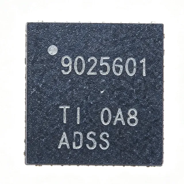
BQ25601RTWR - 3A I2C Buck Battery Charger | Texas Instruments
The Texas Instruments BQ25601RTWR is a highly integrated I2C-controlled 3A single-cell battery charger with Narrow Voltage DC (NVDC) power path management, designed for high input voltage applications. It operates from an input voltage range of 3.9V to 13.5V (14V absolute maximum) and supports a charge current up to 3A, in a 24-pin WQFN (4x4mm) RTW package over -40C to +85C. A battery charger IC is a power management integrated circuit that regulates the charging of rechargeable batteries, ensuring safe and efficient charging while protecting the battery from overvoltage, overcurrent, and overtemperature conditions. Within the power management IC hierarchy, the BQ25601 integrates a synchronous buck converter, NVDC power path management, and an I2C interface, enabling dynamic power management between the input source, system load, and battery. This allows the system to boot and operate even when the battery is deeply discharged or absent. Key features include a 3A fast-charge current, adjustable charge voltage from 3.856V to 4.624V, high input voltage support up to 13.5V, and an integrated bootstrap diode for the high-side gate drive that simplifies system design and reduces BOM count. The I2C serial interface provides programmable charge current, charge voltage, and input current limits, and supports On-The-Go (OTG) boost operation from the battery to power attached USB peripherals. The BQ25601 uses a synchronous buck topology with a high-efficiency power stage, achieving approximately 92% efficiency at typical operating conditions. Input voltage and current regulation (DPM) deliver maximum charging power from USB adapters and other sources, while protections include input overvoltage, battery overvoltage, and thermal shutdown. Typical applications include smartphones, tablets, portable speakers, power banks, and industrial or medical handheld devices requiring reliable high-current single-cell charging with power path management. When designing with the BQ25601, ensure a proper PCB layout with thermal vias under the exposed pad and adequate copper area for heat dissipation at 3A charge currents, and configure I2C registers to set the desired charge parameters. According to TI datasheet (bq25601.pdf), pricing at authorized distributors starts around $0.37 at LCSC as of 2026-08-30.

BQ25703ARSNR - I2C 1-4 Cell NVDC Buck-Boost Charge Controller | TI
The Texas Instruments BQ25703ARSNR is an I2C-controlled, multi-chemistry, 1-to-4 cell NVDC buck-boost battery charge controller with system power monitor and processor hot monitor, housed in a 32-pin WQFN (RSN) 4x4 mm package. It accepts a wide input voltage range of 3.5V to 24V (with 36V absolute maximum transient tolerance on VBUS) and delivers up to 6.35A continuous charge current to the battery, while supplying the system load directly through the integrated NVDC power path. The part supports Li-Ion, Li-Polymer, LiFePO4, lead-acid, NiMH, NiCd and supercapacitor chemistries over the 1.024V to 19.2V battery range. A buck-boost battery charge controller is a power-conversion and power-path-management IC that accepts an input source voltage that may be higher, lower, or equal to the battery voltage, and continuously regulates the charge current and voltage into a multi-cell series battery pack. As a category, it sits within the battery management IC (BMIC) family, itself a subset of power management ICs that handle charging, gauging, protection and authentication for rechargeable energy storage. The BQ25703A family specifically targets USB-C PD, two-port adapter and wide-Vin industrial charging applications that require seamless source/battery load-sharing. Key features of the BQ25703ARSNR include integrated charge, system, and recharging FETs, 1.5MHz programmable switching frequency, integrated 12-bit ADC for voltage, current and temperature telemetry, dynamic power-path management (DPPM) for adapter load sharing, and USB-C PD negotiated-input support up to 20V through the integrated input-current optimizer. The IC also includes a processor hot-monitor function that flags system overheating via I2C status bits and a JEITA-compliant thermal regulation loop that throttles charge current to maintain safe cell temperature. The device uses a peak-current-mode buck-boost architecture with four MOSFETs and an inductor, allowing the converter to operate seamlessly across boost (VIN < VBAT), buck (VIN > VBAT), and pass-through (VIN = VBAT) regions without mode-transition artifacts. The NVDC topology keeps the system rail just above VBAT when input is absent, allowing instant turn-on when the adapter is plugged back in, while the input current optimizer regulates adapter draw to within USB-C PD negotiated limits with sub-100 mA accuracy. Typical applications include 1S to 4S USB-C PD laptop power banks, 2-in-1 detachable notebook chargers, 12V industrial sensor backpacks with supercapacitor buffering, USB-PD multi-port hubs that charge attached devices, and portable medical carts using LiFePO4 battery stacks. The wide chemistry support also makes it suitable for e-mobility kick-scooter and e-bike on-board chargers operating from 36V ebike-bus supplies. When designing with this device, ensure that the input bulk capacitor, the four buck-boost switching-node snubbers, and the battery-side sense resistor are sized per the BQ25703A datasheet typical-application circuit. The PROG pin resistor sets the default battery charge current before any I2C override, and the ILIM pin programs the adapter-side current limit. Both must be populated even when I2C defaults are used. This page synthesizes distributor pricing, drop-in WQFN-32 alternatives, I2C register differences and practical design notes not found in the manufacturer datasheet alone.

BQ25703ARSNT - NVDC Buck-Boost Battery Charger | Texas Instruments
The Texas Instruments BQ25703ARSNT is a synchronous NVDC (narrow-voltage DC) I2C-controlled multi-chemistry buck-boost battery charge controller with system power monitor and processor hot monitor, housed in a 32-pin WQFN (RSN) 4x4 mm package with small 250-unit tape-and-reel packaging. The device charges 1- to 4-cell battery packs from a wide 3.5V to 24V input source (adapters, USB-C PD, solar) and supports multi-chemistry profiles including Li-Ion, LiFePO4, Lead Acid, NiCd, and NiMH. Maximum charge current reaches 8.128A at up to 19.2V output, enabling fast-charging high-capacity packs. The IC integrates a buck-boost topology that delivers seamless transition between boost and buck modes without disturbing the system rail. A buck-boost battery charger is a switching-mode power controller that can either step up (boost) or step down (buck) its input voltage to maintain a regulated output for charging multi-cell battery stacks, regardless of whether the input is above or below the battery voltage. Within the power management hierarchy, the BQ25703A sits at the battery management sub-category alongside fuel gauges and protectors, and within the broader category of battery charging ICs. Its NVDC-1 configuration regulates the system rail at battery voltage but never below a programmable minimum, allowing operation even when the battery is fully depleted. Integrated power-path MOSFET drivers and a high-accuracy 16-bit ADC enable compact, high-efficiency designs. Key features include integrated charging, a system power monitor with input current/voltage MPPT support, a processor hot monitor for thermal throttling signals, and an I2C host interface for telemetry and configuration. The switching frequency is programmable up to 1.5 MHz, enabling small external inductors. Built-in protections cover input overvoltage, battery overvoltage, overcurrent, thermal shutdown, and safety timer. The small WQFN-32 (RSN) footprint suits space-constrained USB-C PD laptops, drones, power tools, and industrial battery packs. The BQ25703A uses a synchronous buck-boost topology with high-side and low-side MOSFET gate drivers and supports both adapter and battery as the system power source. Its NVDC architecture maintains a minimum system voltage (VSYS_MIN) during battery transients, preventing CPU brownouts. The 16-bit ADC provides accurate measurements of input voltage, input current, battery voltage, battery current, system voltage, and die temperature. The integrated MPPT algorithm and processor hot monitor are differentiated features rarely combined in competing parts. Typical applications include 2S-4S USB-C PD laptop chargers, power tool battery packs, drone charging hubs, solar power bank controllers, and portable industrial test equipment. The wide-chemistry and 1-4 cell flexibility make it broadly deployable across consumer and industrial energy storage products. When designing with the BQ25703A, ensure the input capacitor (CIN) and decoupling capacitors are placed close to the IC, and follow the SLUUBO7 schematic checklist for current-sense resistor sizing and inductor selection. The host MCU must initialize the I2C register map before charging begins, and thermal layout should provide sufficient copper area to dissipate 2-3W at full load. This page synthesizes distributor pricing, drop-in alternatives (BQ25703ARSNR, BQ25708RSNT, BQ25700ARSNR, BQ25710RSNT), and practical design notes not found on the manufacturer datasheet alone.
BQ25723RSNR - I2C 1-4 Cell NVDC Buck-Boost Charger | TI
The Texas Instruments BQ25723RSNR is an I2C-controlled 1- to 4-cell narrow VDC (NVDC) buck-boost battery charge controller with integrated system power monitor and processor hot monitor, housed in a 32-pin WQFN (RSN) 4x4 mm package rated from -40C to +125C. It supports Li-Ion/Li-Polymer, LiFePO4, Lead Acid, NiCd, NiMH, and SuperCap chemistries, and integrates USB-C Power Delivery (PD) on-the-go (OTG) plus USB-PD Fast Role Swap (FRS) compliance. A battery charge controller is a power management IC that regulates charging current and voltage into a battery pack while protecting both the battery and the system load. The NVDC power-path architecture separates the system rail from the battery voltage, allowing a system to boot and operate instantly even with a deeply discharged or absent battery. Charge controllers sit at the top of the power hierarchy in portable systems, alongside DC-DC converters, fuel gauges, and battery protection ICs. Key features include the buck-boost charging topology, which charges the battery across the full adapter voltage range regardless of whether VIN is above or below the battery voltage, and an I2C serial interface for full programmability of charge parameters. The integrated system power monitor enables real-time voltage, current, and power telemetry, while the processor hot monitor provides input-current-based throttling signals so the host CPU can reduce load before overloading the adapter. Technically, the BQ25723 uses TI's NVDC architecture with converter-based power path management. The USB-PD Fast Role Swap integration, compliant with the latest USB-C PD specification, ensures that power role swaps in dock and hub applications occur without momentary power loss or glitching at the device under power. This makes the part well-suited to Thunderbolt docks, USB-C monitors, and multi-port charging hubs where source-to-sink transitions must be seamless. Typical applications include USB-C PD docks and hubs, 1-4 cell Li-ion battery-powered notebooks and tablets, portable instruments, and industrial handhelds using Lead Acid, NiMH, or LiFePO4 packs. The wide chemistry support and programmable charge profile let a single PCB design serve multiple battery variants. Design consideration: because the buck-boost converter drives external power MOSFETs and inductor, careful attention to MOSFET selection, inductor saturation current, and thermal layout of the WQFN-32 power path is essential for reliable full-current charging. This page synthesizes distributor availability data, drop-in family alternatives, and practical design notes not found in the manufacturer datasheet. Pricing below is quoted as of 2026-10-16.
BQ25731 - 1-5 Cell NVDC Buck-Boost Charger | Texas Instruments
The Texas Instruments BQ25731RSNR is an I2C-controlled, 1- to 5-cell NVDC (Narrow VDC) synchronous buck-boost battery charge controller with USB Type-C Power Delivery (PD) support, housed in a 32-pin QFN (RSN) package measuring 4 mm x 4 mm. It operates across a wide input range of 3.5 V to 26 V (5 V to 26 V OTG range), charges battery packs from 1 to 5 series Li-ion / Li-polymer / LiFePO4 cells, and integrates USB-C PD 3.0 PPS negotiation for modern Type-C power sources. A buck-boost battery charge controller is a power converter IC that can step up (boost) or step down (buck) the input voltage to match the battery voltage regardless of whether VIN is above, below, or equal to VBAT, eliminating the need for an external boost stage. It belongs to the battery management hierarchy: charger IC -> battery management -> power management IC -> semiconductor. The NVDC topology maintains system rail voltage slightly above the battery, allowing instant system operation even with a deeply depleted or absent battery. Key features include 5 A charging current capability with 80 mA / 4 mA termination steps, integrated 12-bit ADC for system monitoring, JEITA-compliant NTC thermistor input, and an adjustable 3 V to 24 V OTG output with 8 mV resolution for USB-C PD 3.0 PPS applications. The built-in synchronous switching MOSFET drivers deliver high efficiency while minimizing external component count. The architecture combines peak-current-mode control with adaptive compensation, achieving tight regulation across the entire buck, buck-boost, and boost operating regions. Its wide-input tolerance makes it ideal for laptop / ultrabook charging, USB-C hubs, and power tool battery packs that may receive both 5 V USB-PD and 20 V high-voltage adapters. Typical applications include 1- to 5-cell battery charging for notebooks, ultrabooks, tablets, USB-C docking stations, and power-tool battery packs. It is also used in industrial backup batteries, portable medical equipment, and drones that need bidirectional USB-PD functionality. When designing with the BQ25731, ensure the I2C master is connected before power-up to configure charging parameters. Use TI's Battery Management Studio (bqStudio) GUI for initial configuration and debugging, and always consult the manufacturer's datasheet for layout guidelines, including thermal vias under the exposed pad. This page synthesizes distributor pricing, drop-in alternatives (BQ25730), and practical design notes not found in the manufacturer datasheet, providing engineers a single-source reference for evaluation and sourcing.

BQ25798RQMR - 1-4 Cell 5A Buck-Boost Solar Charger IC | TI
The Texas Instruments BQ25798RQMR is an I²C-controlled, 1-to-4-cell, 5-A buck-boost battery charger with dual-input selector and MPPT, housed in a 29-pin VQFN-HR (RQM) 4x4 mm package. It supports 1- to 4-cell Li-Ion, Li-Polymer, and LiFePO4 battery packs with integrated four-switching MOSFETs, BATFET driver, and USB PD 3.0 PPS profile support for input source negotiation. A buck-boost battery charger is a switched-mode DC-DC converter that maintains a stable output voltage even when the input voltage sits below, equal to, or above the battery voltage. BQ25798RQMR sits within the battery management IC family in the broader power management IC category. Compared with buck-only chargers, the buck-boost topology handles wide VIN ranges (such as a depleted solar panel or weak USB source) without a separate pre-boost regulator, reducing BOM and PCB area. Key specifications include 5-A continuous charging current (with parallel charging for higher power), dual-input source selector with MPPT for photovoltaic panels, integrated ADC for input/battery current and voltage monitoring, and high power density through four integrated N-channel MOSFETs. The IC also features an integrated BATFET that supports fast backup mode for UPS-like operation, USB-PD 3.0 PPS compatibility, and I²C programmable parameters including charge voltage, current limits, and switching frequency. The BQ25798 utilizes a four-switch buck-boost topology with current-mode control to deliver high efficiency across the full VIN/VBAT range. The internal gate drivers and dead-time optimization minimize body-diode conduction, while the integrated charge-management engine implements JEITA temperature profiles and thermal regulation. The 29-pin VQFN-HR package provides a low-thermal-resistance path, enabling 5-A charging in a compact 4x4 mm footprint without external FETs. Typical applications include solar-powered USB-C power banks, 2S-4S portable power stations, USB-PD PPS charging docks for power tools, e-bike and e-scooter onboard chargers, and battery backup systems for IoT gateways. The MPPT function targets small photovoltaic panels used in outdoor IoT and consumer solar installations. When designing with this part, provide adequate thermal copper around the exposed pad and follow TI's layout guidelines for high-current buck-boost loops. Use the Battery Management Studio (BQStudio) GUI or host MCU firmware for I²C configuration. This page synthesizes distributor pricing, drop-in alternatives, application notes, and a comparison table against competing TI and third-party solutions beyond the manufacturer datasheet.

BQ25883RGER - 2A 2-Cell Boost Battery Charger | TI VQFN-24
The Texas Instruments BQ25883RGER is a highly integrated 2-A switch-mode boost battery charger designed for 2-cell (2S) lithium-ion and lithium-polymer batteries, housed in a 24-pin VQFN (RGE) 4x4 mm package. It supports a 3.9V to 6.2V input range from a USB or 5-V adapter source, delivers up to 2 A of charge current, and provides I2C-programmable charge voltage, charge current, and input-current-limit settings. The device integrates power-path management so the system can run from the input source, the battery, or both simultaneously. A battery charger is a power-management IC that safely transfers energy from an external DC source (such as a USB port or wall adapter) into a rechargeable battery pack while protecting the cells from over-voltage, over-current, and overheating. Within the broader taxonomy, the BQ25883 sits under battery charger -> battery management -> power management IC -> semiconductor. The "boost" topology means the charger boosts a 5-V input up to the higher 8.0V-8.4V voltage required by a 2-cell Li-ion pack, and it can also function as a boost converter for USB On-The-Go (OTG) mode, supplying 5 V at the input pin from the battery. Key features include USB OTG boost operation up to 2 A, dynamic power-path management (DPPM), input current optimizer (ICO), and an integrated 12-bit ADC for monitoring bus voltage, battery voltage, charge current, and die temperature. The BQ25883 also supports adjustable thermal-regulation thresholds and JEITA-style battery-temperature sensing via an NTC pin, making it suitable for safety-conscious portable products. Architecturally, the device combines a synchronous boost switching converter (operating at up to 1.5 MHz), a high-accuracy I2C-programmable battery-regulation loop, and a low-resistance power path. A single inductor and small ceramic capacitors complete the power stage, allowing compact PCB designs for handheld and wearable applications. Typical applications include 2S Li-ion power banks, 2S portable medical monitors, USB-C tablets, 2S handheld vacuum cleaners, and Bluetooth speakers. The OTG boost capability also lets the device act as a 5-V supply for downstream accessories. When designing with the BQ25883, ensure the input capacitor, output capacitor, and inductor are placed close to the IC and that the thermal pad is soldered to a sufficient copper pour for 2-A continuous charging. Use the I2C interface to set charge voltage, current, and input-current limits per the host processor's power-budget policy. This page synthesizes distributor pricing, parametric drop-in alternatives, and practical design notes not found in the manufacturer datasheet alone.
BQ27421-G1 - System-Side Impedance Track Fuel Gauge | TI
The Texas Instruments BQ27421-G1 is a system-side Impedance Track fuel gauge with integrated 7 mΩ current-sense resistor for single-cell Li-Ion battery packs, housed in a 9-ball DSBGA (YZF) package. It reports remaining capacity (mAh), state-of-charge (%), battery voltage, current, temperature, and runtime via an I2C interface, requiring minimal host microcontroller firmware development. Key specifications include a 4.2 V maximum charge voltage (chemistry profile A), integrated 7 mΩ sense resistor between the BAT and SRX pins, I2C communication up to 400 kHz, and ultra-low quiescent current suitable for always-on battery monitoring. The device operates directly from the cell it monitors, eliminating the need for an external regulator rail. Its Impedance Track algorithm models cell impedance to deliver accurate state-of-charge estimation across varying load, temperature, and aging conditions without requiring board-level calibration. The BQ27421-G1 belongs to the fuel gauge / battery monitor IC category within the power management IC hierarchy. As a system-side gauge (mounted on the host board rather than inside the battery pack), it is designed for applications where the battery pack is not a smart pack but accurate fuel gauging is still required. Its integrated sense resistor eliminates the precision external shunt that traditional coulomb-counting solutions require, reducing BOM cost and PCB area while improving current-sensing accuracy at low loads. Typical applications include smartphones, wearables, portable medical devices, Bluetooth headsets, and single-cell Li-Ion powered IoT endpoints where reporting remaining runtime to the user matters. The wide chemistry support — pre-programmed profiles such as 4.2 V, 4.3 V, and 4.35 V, indicated by the suffix letter (A, B, etc.) — lets designers match the gauge to the cell's full-charge voltage without firmware rework. When designing with this part, route the BAT and SRX traces as a Kelvin connection directly to the integrated sense-resistor balls to avoid parasitic IR drop, and keep the DSBGA balls clear of flux contamination during reflow. Always select the chemistry variant (e.g. BQ27421YZFR-G1A for 4.2 V, -G1B for 4.3 V, -G1C for 4.35 V) that matches the cell's maximum charge voltage to avoid over-reporting SOC. This page consolidates verified distributor pricing, drop-in chemistry-variant alternatives in the same DSBGA footprint, and practical PCB-layout notes that go beyond what the manufacturer datasheet alone covers.
BQ27421YZFR-G1A - System-Side Fuel Gauge w/ Integrated Sense Resistor | Texas Instruments
The Texas Instruments BQ27421YZFR-G1A is a system-side Impedance Track fuel gauge IC with an integrated current-sense resistor, designed for single-cell Lithium-Ion and Lithium-Polymer battery packs. Housed in a 9-ball DSBGA (YZF) package, it operates from 2.45V to 4.5V supply, supports I2C communication, and provides accurate state-of-charge, remaining capacity, and runtime reporting with minimal host-side firmware. A battery fuel gauge is a category of battery management IC that estimates the state-of-charge (SOC) of a rechargeable battery by combining voltage, current, and impedance measurements. As a sub-category of battery monitors and gas gauges, it sits within the broader battery management hierarchy of power management ICs, ultimately belonging to the semiconductor product tree used in portable and embedded systems. The BQ27421YZFR-G1A features TI's patented Impedance Track algorithm, which adapts to cell aging and provides accurate SOC reporting without requiring a full charge-discharge characterization cycle. The integrated sense resistor eliminates the need for an external shunt, simplifying PCB layout and reducing BOM cost. The device reports remaining capacity (mAh), state-of-charge (%), voltage, current, and temperature over the standard I2C interface, supporting SMBus-compatible commands. Typical applications include wearables, fitness bands, portable medical devices, Bluetooth headphones, smart pens, single-cell Li-Ion powered IoT endpoints, and compact handheld instrumentation where board space is constrained and a separate shunt resistor is undesirable. When designing with the BQ27421YZFR-G1A, ensure the I2C lines have appropriate pull-up resistors (typically 10kohm to VCC) and follow the layout guidelines for the DSBGA thermal pad to maximize thermal dissipation and mechanical reliability. A 0.1uF decoupling capacitor close to the BAT pin is required, and the device should be the only battery monitor on the I2C bus at address 0x55 unless address reprogramming is performed. This page consolidates the BQ27421YZFR-G1A's datasheet parameters, drop-in alternatives, and practical design guidance not typically aggregated on a single distributor page, enabling engineers to quickly assess fit for their next single-cell Li-Ion design.
BQ29707DSER - Li-Ion/Li-Po Single-Cell Battery Protector | TI
The Texas Instruments BQ29707DSER is a cost-effective voltage and current protection IC for single-cell Li-Ion and Li-Polymer batteries, integrating the full secondary protection chain into a compact 6-pin WSON (DSE) package measuring 1.5 mm x 1.5 mm with 0.5 mm terminal pitch. It delivers fixed overcharge, overdischarge, overcurrent (charge/discharge), and short-circuit thresholds optimized for the BQ29707 configuration, eliminating the need for an external MCU supervisor. The device operates directly from the cell and drives external N-channel MOSFETs that disconnect the pack from the system during a fault. A battery protection IC (often called a "secondary protector" or "battery management IC for protection") sits between a single Li-Ion/Li-Po cell and the host load. It continuously samples the cell voltage through Vdd and the pack current through the voltage drop across the external FETs (Vds sensing). When a fault threshold is crossed, the device latches off or releases the charge (CHG) and discharge (DSG) FET gates, isolating the cell to prevent fire, swelling, or capacity loss. The BQ2970 family is the cost-down alternative to TI's higher-feature fuel gauges such as the BQ28z610 and BQ34z100, and pairs naturally with the BQ27421-G1A gauge IC for smart-pack designs. Key features include a 0 V charge-disabled function, a wide operating temperature range from -40 °C to +85 °C, factory-trimmed thresholds requiring no external programming resistors, and ultra-low quiescent current in both normal and power-down modes. The part offers overcurrent detection on both charge and discharge paths and dedicated short-circuit protection with sub-millisecond response, all on the same die. Internally the BQ29707DSER uses a precision bandgap reference and a comparator ladder matched to the cell chemistry. The FET driver is a charge-pump architecture capable of holding the external N-FET gates above Vdd during normal operation while pulling them to ground rapidly when a fault is triggered. The result is a single-chip protector with predictable behavior across the full cell state-of-charge window. Typical applications include single-cell smart-phone spare batteries, wearable packs, TWS earbud charging cases, IoT sensor nodes, and any compact single-cell Li-Po pack that previously used a discrete comparator + dual-FET protection circuit. The 6-WSON footprint suits 1S packs with board space below 4 mm x 4 mm. When designing, ensure the external N-FETs are logic-level types with low gate threshold, and add an RC snubber on Vdd close to the IC to ride out load transients. The 0 V charge inhibit is factory-set and cannot be disabled; verify that it matches your charger requirements. This page synthesizes distributor stock and pricing, drop-in pin-compatible alternatives, and practical layout notes not found in the manufacturer datasheet.

BQ2982 - High-Side 1S Li-Ion Protector with Charge Pump | Texas Instruments
The Texas Instruments BQ2982 is a high-side single-cell Li-ion/Li-polymer battery protector featuring an integrated charge-pump NFET driver, overvoltage, undervoltage, overcurrent during charge (OCC), overcurrent during discharge (OCD), short-circuit during discharge (SCD), and zero-volt recovery support, housed in a compact 8-pin X2QFN (1.5 mm × 1.5 mm) package. Headline parameters include ±10 mV typical overcurrent detection accuracy, support for sense resistors as low as 1 mΩ, and a 1-series (1S) Li-ion/Li-polymer cell configuration. What is a battery protector? A battery protector is a dedicated safety IC that monitors a rechargeable cell's voltage, current, and temperature, and disconnects the cell from the load or charger when an unsafe condition is detected. Within the broader taxonomy, the BQ2982 is a single-cell Li-ion protector, a sub-category of battery management ICs (BMICs), which themselves sit under power management semiconductors. Compared with general-purpose fuel-gauge ICs, protectors focus on fast hardware-level cutoff rather than coulomb counting. Key features include the high-side NFET drive architecture (which keeps the protection FETs on the positive rail for simpler PCB layout and lower Rdson sensitivity to cell voltage), the integrated charge pump that maintains a constant VGS across the protection FET regardless of cell state-of-charge, and tight overcurrent thresholds that allow designers to use very low-value sense resistors (1 mΩ) for improved thermal efficiency. The X2QFN package footprint is among the smallest available for primary protection ICs, suiting space-constrained wearables and phones. Technically, the BQ2982 uses a precision bandgap reference, a temperature-compensated current-sense comparator, and programmable delay timers (latch or auto-recover modes). The device supports both latched and auto-recovery output modes, allowing system designers to choose between hard shutdown (e.g., for SCD) and recoverable fault clearing (e.g., for temporary overload). Communication with the host is non-existent on this dedicated protector - all configuration is hardware-strapped via external resistors. Typical applications include smartphones, tablets, power banks, wearables, TWS earbud charging cases, and other single-cell Li-ion/Li-polymer battery packs where high-side switching and ultra-low quiescent current are required. The device is also used in flash/fast-charging architectures where the high-side drive allows the system to maintain consistent FET Rdson during high inrush events. When designing with the BQ2982, ensure the CTLC pin capacitor value matches the desired fault delay timing per the datasheet formulas, and use Kelvin-sense routing between the SRP/SRN pins and the sense resistor to preserve overcurrent accuracy. Always include TVS protection across the cell terminals and place the protector close to the cell to minimize parasitic inductance. This page synthesizes distributor pricing, drop-in alternatives from the BQ298xx family, and practical design notes not found in the manufacturer datasheet alone, giving a complete procurement and design reference for the BQ2982.

BQ34210IPWRQ1 - Automotive 1-Series CEDV Fuel Gauge | TI
The Texas Instruments BQ34210IPWRQ1 is an automotive-qualified 1-series cell system-side CEDV (Compensated End-of-Discharge Voltage) fuel gauge with integrated End-of-Service (EOS) determination, housed in a 14-pin TSSOP (PW) package. The device provides State-of-Charge (SOC), State-of-Health (SOH), and runtime predictions for single-cell Li-Ion, LiFePO4, and NiMH battery packs that experience infrequent discharge cycles such as eCall backup batteries and UPS systems. A battery fuel gauge is a mixed-signal IC that estimates remaining capacity and battery health by combining coulomb counting with voltage, current, and temperature measurements. Within the broader power-management hierarchy, the BQ34210-Q1 sits in the Battery Management category, complementing chargers and protection switches. Unlike impedance-tracking gauges that demand frequent load cycles to remain accurate, the CEDV algorithm is specifically tuned for batteries that sit at near-full charge for long periods, making it a specialized alternative to TI's bq27xxx Impedance Track family. Key specifications include a 14-pin TSSOP (PW) footprint, I2C communication for host MCU access, support for 1-series cell chemistries (Li-Ion / LiFePO4 / NiMH), and an automotive-grade temperature range. The device draws minimal current during periodic wake cycles to update self-discharge compensation, maintaining accurate remaining capacity even after months of float-charge operation. End-of-Service detection flags batteries whose impedance or capacity degradation indicates imminent failure. The BQ34210-Q1 features an integrated sense resistor interface, programmable alarm outputs for low-battery and EOS conditions, and compatibility with TI's Battery Management Studio (bqStudio) for parameter configuration. Its compact TSSOP-14 footprint minimizes PCB area in space-constrained modules such as telematics control units and emergency-call backup packs. Typical applications include automotive eCall backup batteries, asset tracking device primary cells, UPS backup modules, medical device standby batteries, IoT sensor nodes, and emergency lighting battery packs. The EOS prediction function allows fleet operators to replace batteries proactively before they fail in service. When designing with the BQ34210-Q1, ensure the sense resistor value is correctly programmed into the device's data flash to match the application load range. Account for I2C pull-up resistors on the host interface, and verify the thermistor beta and configuration match the chosen cell chemistry. This page synthesizes distributor pricing, drop-in alternatives, application notes, and design guidance not aggregated on a single manufacturer page, including same-package options and practical integration tips.
BQ40Z80RSMR - 2-6S Li-Ion Battery Pack Manager | Texas Instruments
The Texas Instruments BQ40Z80RSMR is a fully integrated 2-series to 6-series Li-ion and Li-polymer battery pack manager with Impedance Track™ gas gauging in a 32-pin VQFN (RSM) 4x4 mm package. It combines analog protection, gauging, cell balancing and authentication in a single chip, targeting 5 V to 24 V battery packs used in power tools, e-bikes, UPS, medical carts, and 1- to 6-cell portable equipment. A battery pack manager is the heart of a smart battery; it measures individual cell voltages, pack current, and temperature, then derives remaining capacity and state-of-health while enforcing protection limits. The BQ40Z80 belongs to the category hierarchy battery management IC > gas gauge + protector > battery pack manager > power management IC, complementing the charger and protection MOSFETs in the system. Impedance Track is TI's patented coulomb-counting-plus-modeling approach that learns cell impedance at every cycle to deliver accurate runtime prediction even under varying loads and aging. Key features include 2S to 6S cell support, integrated CC-CV charge profile control via SMBus, hardware secondary protection, 18-bit integrated delta-sigma A/D for cell voltage measurement, on-chip cell balancing drivers, SHA-1/ECC authentication with secure memory, and eight multifunction pins configurable as thermal inputs, GPIO, LEDs, or display-button. Integrated sense resistors and a high-side N-FET drive architecture simplify protection MOSFET selection. The device communicates over SMBus v1.1 with optional 400 kHz I²C compatibility and offers an LED display driver for 4- or 5-segment SOC indication. On-chip non-volatile memory stores chemistry profiles, learned parameters, and a 64-bit pack ID for traceability. The 4x4 mm QFN footprint enables compact pack designs while providing a thermal pad for heat spreading during high-discharge balancing. Typical applications include cordless power tool packs, robotic vacuum cleaners, e-bike and e-scooter battery packs, medical infusion pumps, and hot-swap server backup modules. The wide 4.5 V to 32 V operating range tolerates the inductive transients common in motor-driven systems. Designers select the BQ40Z80 when an integrated gauge+protector+authenticator saves PCB area versus discrete solutions like separate AFE plus MCU. When designing, observe the SMBus address selection pin to avoid collisions with a system charger, and follow the cell-balancing resistor sizing in the datasheet to keep balance current within thermal limits. Pair this gauge with TI's BQ25620 charger IC for a complete pack+system solution. This page synthesizes distributor pricing, drop-in alternatives within the same 32-VQFN package, and practical design notes not found in the manufacturer datasheet.

BQ40Z80RSMT - 2-6S Li-Ion Battery Pack Manager | TI
The Texas Instruments BQ40Z80RSMT is a fully integrated, single-chip 2-series to 6-series Li-ion and Li-polymer battery pack manager that uses TI's Impedance Track™ technology for accurate gas gauging, housed in a 32-pin VQFN (4x4 mm) package with exposed thermal pad. A battery management IC (BMIC) such as the BQ40Z80RSMT belongs to the broader category of power management semiconductors. It combines a precision analog front end, an MCU core, non-volatile memory, and firmware-based gas gauging algorithms. The Impedance Track™ family sits hierarchically under fuel gauge IC -> battery management IC -> power management -> mixed-signal semiconductor, and is designed to compute remaining battery capacity using cell voltage, current, temperature and a learned impedance model rather than simple coulomb counting. Key features of the BQ40Z80RSMT include support for 2S to 6S cell packs, integrated cell balancing, programmable protection thresholds (over-voltage, under-voltage, over-current, short-circuit, over-temperature), SHA-1/HMAC authentication for security, a 16-bit delta-sigma ADC for voltage and current measurement, and an I²C/SMBus-compatible communication interface. The device supports host-side charging control via SMBus and reports state-of-charge, state-of-health, runtime, cycle count and cell voltages through standard SBS commands. Technically, the part operates from a battery stack of up to 25.2 V nominal (6S Li-ion fully charged), with internal LDOs generating the logic and analog supplies from the pack. Its Impedance Track™ algorithm dynamically learns each cell's chemistry behavior, allowing reported remaining capacity to track within 1% accuracy under most operating conditions. The compact 32-VQFN footprint reduces board area, while the exposed pad provides the low thermal resistance needed for sustained high-current discharge. Typical applications include multi-cell battery packs for notebook computers, power tools, e-bikes, e-scooters, UPS backup systems, medical carts, and 12V/18V/24V portable equipment. The integrated authentication makes the BQ40Z80RSMT well suited to OEM-branded packs where clone prevention matters. When designing with the BQ40Z80RSMT, allocate a low-impedance ground return for the sense resistor and route the cell-balance FETs to minimize parasitic conduction paths. Follow TI's BQ40Z80 EVM layout exactly when reusing cell-balancing, NTC thermistor and FET-driver sections to pass TI's validated gas-gauging cycle tests. This page synthesizes real distributor pricing, drop-in same-brand alternatives, and practical design considerations drawn from the BQ40Z80 datasheet and reference manual — content not bundled on any single manufacturer or distributor product page.
BQ41Z50RSNR - 2-4S Cell Battery Pack Manager, Dynamic Z-Track | TI
The Texas Instruments BQ41Z50 (BQ41Z50RSNR) is a fully integrated, single-chip battery pack manager with Dynamic Z-Track technology that supports 2-series, 3-series, and 4-series Li-ion, LiPO, and LiFePO4 battery packs. It combines gas gauging, hardware protection, cell balancing, and authentication in a 32-pin QFN (4x4 mm, RSN) package, and runs on an ultra-low-power 32-bit RISC processor with integrated high-performance analog peripherals. A battery fuel gauge IC (also called a battery management IC, gas gauge, or pack manager) is a mixed-signal SoC that monitors cell voltage, current, and temperature to compute State-of-Charge (SOC) and State-of-Health (SOH) while enforcing safety limits for charge, discharge, short-circuit, and over-temperature events. Battery management ICs sit within the hierarchy: battery management IC -> power management IC -> semiconductor device. Key features of the BQ41Z50 include Dynamic Z-Track adaptive impedance learning, which updates impedance tracking during real load transients for tighter SOC accuracy, plus integrated charge/over-discharge/over-current/overtemperature protection, SHA-1 authentication, and support for 2S-4S multi-chemistry cell configurations. The integrated analog front end includes a 16-bit delta-sigma coulomb counter and a high-accuracy ADC for cell voltage measurements. Typical applications include portable power banks, power tools, e-bike and e-scooter battery packs, medical infusion pumps, telecom backup batteries, and any 2S-4S Li-ion/LiFePO4 pack that needs high-accuracy gauging with hardware safety protection. Designers use the BQ41Z50EVM evaluation module and TI's Battery Management Studio (bqStudio) GUI for firmware development and chemistry tuning. When designing with this device, ensure each cell input has an RC filter for noise rejection, follow TI's reference layout for the high-current ground return, and use TI's bqStudio to configure chemistry parameters and protection thresholds. Compared with BQ40Z50-R5, the BQ41Z50 firmware format is not interchangeable per the TI E2E forum; verify replacement firmware before reuse. This page synthesizes distributor pricing, drop-in alternatives, and practical design notes not found in the manufacturer datasheet alone, including same-brand variants and verified pin-compatible substitutes.

BQ41Z90 - 3-16 Cell Battery Fuel Gauge with IT-DZT | TI
The Texas Instruments BQ41Z90 is a highly integrated 3-to-16 series cell battery pack manager that combines a flash-programmable 32-bit processor, hardware protection, and integrated SHA-1/SHA-2/EC-KCDSA authentication responder in a single IC. According to the manufacturer datasheet, the device supports Li-ion, LiFePO4, NiMH, and Li-polymer chemistries across stacks of 3 to 16 cells in series, with communications handled by SMBus v3.2 or I2C-compatible interfaces. A battery fuel gauge is a type of battery management IC (BMIC) that estimates the remaining state-of-charge (SoC), state-of-health (SoH), and runtime of a rechargeable battery pack by coulomb counting, voltage tracking, and impedance-based modelling. The BQ41Z90 sits in the hypernym hierarchy battery fuel gauge -> battery monitor -> battery management IC -> power management IC -> semiconductor. The TI IT-DZT (Impedance Track with Dynamic Z-Track) algorithm extends standard Impedance Track technology by capturing cell impedance under dynamic load profiles, which improves accuracy during transients such as EV acceleration pulses or power-tool bursts. Key features include an ultra-low-power high-speed 32-bit processor core, on-chip flash for application firmware, hardware-based safety protection including over-voltage, under-voltage, over-current, short-circuit, and overtemperature comparators, an NMOS protection FET driver, ECC (elliptic-curve cryptography) authentication, and integrated protection FET drivers. The device integrates an array of peripheral I/O and supports both high-side and low-side N-FET protection topologies with configurable thresholds stored in on-chip flash registers. The BQ41Z90 architecture combines an ARM Cortex-M0-class 32-bit core, a high-accuracy coulomb counter ADC, a 16-bit voltage ADC for cell-stack telemetry, on-die temperature sensors, and a dedicated authentication block that responds to host-side SHA-1, SHA-2, or EC-KCDSA challenges. Per the datasheet, this combination eliminates the external MCU + dedicated AFE two-chip approach used in legacy designs and reduces BOM by approximately 30 percent. Typical applications include multi-cell power banks, e-bikes and e-scooters, power tools, robotics battery packs, e-mobility and light-EV battery packs, and uninterruptible power supply (UPS) battery modules that require both accurate fuel gauging and pack-level hardware protection. When designing with the BQ41Z90, observe that this part requires TI's BQStudio configuration tool for golden-image flash programming and that production authentication keys must be provisioned per the TI security lifecycle flow. Plan for the WAKE pin behaviour referenced in the datasheet section 7.3.1.2.2.4 and add an external pull-up if the application idles in shipping mode. This page synthesizes distributor pricing, parametric comparison tables, drop-in alternatives, and practical design notes that go beyond what is published in the manufacturer datasheet PDF.

BQ500210RGZT - Qi Wireless Power Transmitter Manager | Texas Instruments
The Texas Instruments BQ500210RGZT is a second-generation, Qi-compliant wireless power transmitter manager with a 110 kHz to 205 kHz operating-frequency range, a 3 V to 3.6 V supply range, and a 48-VQFN 7 mm × 7 mm package. It is designed to control a single-channel wireless power transfer system in a contactless charging base station. A wireless power transmitter manager is a specialized power-management IC that coordinates sensing, communications, pulse-width modulation, and power-stage control for wireless charging equipment. Its hierarchy is wireless power controller, transmitter controller, power-management IC, and semiconductor. Unlike a general-purpose buck converter, this device is intended to manage an inductive power-transfer link operating under wireless-power-consortium protocols. The verified product information identifies the BQ500210 as an IF transmitter and a dedicated digital controller that periodically pings the surrounding environment for devices available for powering and monitors communication from the power receiver. Its Qi compliance and communication-monitoring functions help the base station detect receiver presence, exchange required control information, and adjust the wireless-power operating process. The controller operates from 3 V to 3.6 V and supports an operating-frequency range of 110 kHz to 205 kHz. Its 48-VQFN package is suitable for compact transmitter-PCB designs. The exposed-pad construction provides a thermal and electrical land-pattern requirement that must be implemented according to the manufacturer datasheet rather than treated as an ordinary 48-lead non-exposed package. Typical uses include Qi-compatible charging pads, embedded wireless charging surfaces, sealed charging products, furniture-integrated chargers, and hermetically sealed devices. Because the part is specifically intended for hermetically sealed devices and single-channel base stations, system-level matching between the controller, transmitter driver, resonant tank, receiver, and coil is essential. When laying out a transmitter board, preserve the recommended power and signal-loop topology and place high-current switching paths compactly. Keep sensitive communication and sensing paths away from resonant-current edges, use the manufacturer-recommended thermal-pad implementation, and validate the final coil, driver, switching frequency, and receiver combination rather than assuming that functionally similar controllers are interchangeable. This page consolidates the verified Texas Instruments product description, distributor listing information, package details, operating ranges, and cross-reference findings. It also separates verified facts from missing electrical details and avoids presenting unverified alternatives as drop-in replacements, helping engineers identify what must still be checked against the manufacturer datasheet.
BQ500414Q - Automotive Qi Wireless Power Controller | Texas Instruments
The Texas Instruments BQ500414Q is an AEC-Q100 qualified automotive-grade digital wireless power controller designed for Qi-compliant free-positioning wireless charging systems. It is available in a 48-pin VQFN (7x7 mm) package and operates over a temperature range from -40°C to 85°C, making it suitable for automotive environments. The controller implements the WPC v1.1 A6 transmitter specification and is optimized for 12-V supply systems, though it can support other supply voltages. What is a wireless power controller? A wireless power transmitter controller is a specialized power management IC that manages the power transfer between a transmitter and a receiver using inductive coupling. It coordinates the coil switching, modulates the power signal, and communicates with the receiver through the Qi protocol to ensure safe and efficient charging. The BQ500414Q simplifies designs by integrating the control logic, I2C interface, and LED drive outputs, reducing the external component count and system complexity. Key features of the BQ500414Q include direct driving of three LED outputs through pins 7, 8, and 9 using a simple current-limit resistor (typically 470 ohms), which provides visual status indication without additional driver ICs. The I2C interface enables communication with host controllers, allowing system-level monitoring and configuration. The free-positioning capability of the controller supports multi-coil arrangements, enabling convenient placement of receivers on the charging surface. The BQ500414Q is designed for automotive applications where robustness and reliability are critical. Its AEC-Q100 qualification ensures it meets stringent automotive quality standards. The device is WPC v1.1 ready, conforming to the Qi wireless charging standard for interoperability with compliant receivers. The transmitter type A6 specification defines the coil geometry and power transfer characteristics, and the controller is optimized for 12-V systems, which are common in automotive power architectures. Typical applications include in-cabin wireless phone chargers, aftermarket charging pads, and industrial or medical devices requiring wireless power. The device's EEPROM-programmable parameters allow customization for specific system requirements, and the integrated LED drivers simplify user feedback. When designing with this controller, pay careful attention to the thermal management of the power stage and the layout of the coil driver circuitry, as these directly influence charging efficiency and EMI performance.

BQ51013A - Qi Wireless Power Receiver PMIC | TI
The Texas Instruments BQ51013A is an integrated Qi-compliant (WPC 1.1) wireless power receiver IC that performs AC/DC power conversion in a 20-pin VQFN (3.5x4.5 mm, RHL) package. Per TI datasheet SLUSBA2, the device delivers a regulated 5V output from the receiver coil with up to 1.5 A output current and reaches 93% overall peak AC-DC efficiency, eliminating the need for a separate rectification stage plus LDO combination. Qi wireless charging is a tightly-coupled inductive power transfer method standardized by the Wireless Power Consortium (WPC). A transmitter (TX) coil generates an alternating magnetic field at ~110-205 kHz, and a receiver (RX) coil coupled to that field induces an AC voltage which the receiver IC must rectify, regulate, and present as a clean DC rail. The BQ51013A integrates the full receiver signal chain: synchronous rectification, dynamic rectifier voltage control, communication demodulation, and a 5V LDO post-regulator, so engineers can power a load or feed a downstream charger with one part. Key features include a built-in I2C interface for status reporting, dynamic power limiting (DPL) to handle thermal constraints, and foreign-object detection (FOD) compliance per the WPC Qi specification. The IC supports Qi 5W baseline power profiles and operates from the rectified coil voltage (RECT pin) up to 7V, with over-voltage, over-current, and thermal-shutdown protections. Communication back to the TX is handled through load modulation and a single-bit demodulator, providing the WPC-defined packets required for authentication and power control. The architecture combines a full-bridge synchronous rectifier with a hysteretic-mode buck converter to produce the regulated 5V output. Adaptive rectifier voltage control keeps the rectifier just above the input to maximize efficiency across load and coupling variations, and the integrated 5V LDO with low-dropout performance ensures a low-noise rail for downstream ICs. FOD is implemented via Q-factor measurement of the resonant tank before and during power transfer, allowing the part to detect metal objects that would otherwise overheat. Typical applications include Qi wireless charging pads for smartphones and wearables, medical-device charging cradles, low-power IoT charging stations, and any portable product requiring cable-free charging from a WPC-compliant transmitter. Design considerations include coil selection (the WPC A11/A6a coil is the most common reference design), thermal management of the receiver PCB, and proper I2C address configuration when multiple receivers share a bus.
BQ51013C-Q1 - 5W Qi Wireless Power Receiver | Texas Instruments
Texas Instruments BQ51013C-Q1 is an automotive, fully integrated wireless power receiver PMIC with up to 5 W of delivered output power, WPC v1.3 communication control, and a 20-pin VQFN package measuring 3.5 mm by 4.5 mm. The device combines receiver AC-to-DC conversion, a low-resistance synchronous rectifier, an LDO, digital control, and voltage and current loops in one IC. Its integrated architecture supports portable wireless-charging products and is qualified for automotive applications according to the verified component listing. A wireless power receiver is the secondary-side device in an inductive charging system. It receives energy from a transmitter through a receiver coil, converts the alternating coil voltage into a regulated DC output, and communicates with the transmitter. The BQ51013C-Q1 places the Qi communication protocol, rectification, regulation, and control functions between the receiver coil and the powered load, reducing the number of external ICs required for a Qi v1.3 receiver design. The verified manufacturer material highlights a 93% peak AC-DC efficiency target in the family datasheet text, full synchronous rectification, accurate voltage and current loops, and output-voltage conditioning. These features are relevant when designing a compact receiver whose power loss can become heat inside a phone, accessory, or automotive console. The Q1 device is intended for automotive wireless-power applications, while the product-family information identifies the BQ51013C family as delivering up to 5 W. Typical applications include 5 W wireless charging for portable devices, automotive center-console charging pads, accessory power for battery-operated products, and embedded wireless-power modules where the receiver IC must sit close to a coil and provide controlled DC output. The receiver-side architecture is important: coil coupling, alignment, thermal conditions, communication timing, output loading, and the downstream power path all affect the user experience. For implementation, follow the manufacturer datasheet for the RHL package pinout, recommended coil and capacitor values, PCB layout, thermal design, and communication timing. Do not infer unverified electrical limits or pin functions from a distributor listing. This page combines verified manufacturer and distributor information with engineering-oriented selection and design guidance; current pricing, stock, and detailed electrical values must be confirmed against the cited sources.
BQ51013CQWRHLRQ1 - 5W WPC 1.3 Wireless Power Receiver | Texas Instruments
The Texas Instruments BQ51013CQWRHLRQ1 is an automotive-qualified, fully integrated wireless power receiver IC compliant with the Wireless Power Consortium (WPC) Qi v1.3 protocol, housed in a 20-pin VQFN-HR (RHL) package measuring 3.5 mm x 4.5 mm. It delivers up to 5 W of output power on its secondary side, integrating AC-to-DC rectification, digital control, and Foreign Object Detection (FOD) on a single die, and is qualified to the AEC-Q100 standard for automotive applications. The device operates across an input voltage window that supports the Qi coil interface and produces a regulated output suitable for direct battery charging or downstream power rails. A wireless power receiver (sometimes called a Qi receiver or inductive charging Rx) is a specialised power management IC that converts the AC voltage induced in a receiver coil by a wireless charging transmitter into a stable DC output voltage. Receivers sit at the bottom of the power management hierarchy as application-specific PMICs, distinct from general-purpose LDOs, buck converters, and battery chargers. Modern WPC-compliant receivers such as BQ51013C-Q1 also handle the bi-directional Qi communication protocol used by the transmitter to control power transfer, run object detection, and negotiate foreign objects in the magnetic field. Key features include integrated low-loss synchronous rectification, dynamic rectifier clamp voltage adjustment for foreign object detection (FOD), adaptive communication modulation, and a programmable output voltage up to roughly 5 V. The device supports resonant frequency tuning, over-temperature protection, and an adjustable end-of-charge behaviour. Its 3.5 mm x 4.5 mm 20-pin VQFN-HR (RHL) footprint with a thermal pad enables compact PCB integration in space-constrained automotive cabin and console modules. The BQ51013CQWRHLRQ1 uses TI's mixed-signal CMOS architecture, combining a high-efficiency rectifier, a digital state machine that speaks Qi v1.3, and an adaptive comm-link receiver for load modulation. FOD is implemented by comparing transmitted and received power and using a Qi-defined reference to flag metallic foreign objects in the magnetic field before they heat up. Typical applications include automotive Qi wireless charging pads, in-cabin phone charging trays, eMobility accessories, and Qi-certified accessories for infotainment systems. The wide operating range also suits industrial Qi charging cradles and medical device charging bases that demand a regulated, safe power rail. When designing with the BQ51013CQWRHLRQ1, observe the LC tank tuning guidance in the datasheet to align the receiver coil inductance with the Qi specification; the matching network on the output is the single most important factor in achieving a clean 5 V output at full load. Also account for thermal dissipation on the RHL exposed pad - a 4-layer PCB with copper thermal vias is recommended at 5 W continuous output. This page synthesises distributor pricing, drop-in same-brand variants, cross-brand Qi receiver alternatives, and design notes not found verbatim in the manufacturer datasheet.
BQ51013CRHLR - 5W Qi v1.3 Wireless Power Receiver | Texas Instruments
The Texas Instruments BQ51013CRHLR is a fully integrated wireless power receiver PMIC for secondary-side portable-device charging, delivering up to 5W through a WPC Qi v1.3-compatible interface from a 20-pin RHL VQFN package. The verified product data identifies a 3.5 mm by 4.5 mm package, an operating range of -40 °C to 125 °C, and up to 93% overall peak AC-DC efficiency. It combines receiver AC-DC conversion, synchronous rectification, output-voltage conditioning, and digital communication control, allowing the receiver IC to sit between the RX coil and regulated output. A wireless power receiver is the secondary-side device in an inductive charging system. It receives alternating energy from a transmitter coil, converts that energy to DC, regulates the output, and communicates with the transmitter to establish and maintain Qi power transfer. Within the hierarchy wireless power receiver -> power management IC -> battery-management subsystem -> portable-device charger, the BQ51013CRHLR concentrates the power-conversion and negotiation functions needed for a compact receiver design. The verified data lists full synchronous rectification, output-voltage conditioning, WPC v2.0 communication control in one search result, and WPC Qi v1.3 compliance in the Texas Instruments product listing. Only one IC is required between the receiver coil and output according to the indexed datasheet description. These features can reduce external circuitry and simplify portable-device charger development while supporting a maximum output class of 5W. The receiver architecture uses an integrated rectification and regulation stage rather than relying on a discrete diode and separate regulator implementation. Full synchronous rectification can reduce conduction loss compared with a simple diode path, while the reported 93% peak efficiency quantifies conversion performance at its best operating point. Actual efficiency depends on coil coupling, input power, output voltage, load, temperature, and PCB layout, so the peak rating should not be treated as a constant under every condition. Typical uses include 5W wireless charging for wearables, earbuds, mobile accessories, and portable consumer products. The compact package supports space-constrained receiver hardware, while the -40 °C to 125 °C specified temperature range covers industrial-temperature design needs. A product designer still must validate the selected receiver coil, output network, thermal performance, foreign-object behavior, and enclosure geometry. The primary design consideration is preserving coil coupling and high-frequency electrical performance. Follow the manufacturer layout guidance, keep the receiver coil and compensation network close to the IC, provide the required output capacitance, and route high-current paths with minimal loop area. Wireless-power efficiency is a system result involving the transmitter, coil, alignment, shield, load, and board implementation, not only the receiver IC. This page consolidates the verified distributor listings, Texas Instruments product information, package details, efficiency claims, pricing indication, and design considerations into one engineering reference. It also clearly separates verified facts from unavailable specifications and avoids presenting unverified substitute parts as drop-in replacements.
BQ51050B - Qi Wireless Power Receiver & Li-Ion Charger | TI
The Texas Instruments BQ51050B is a Qi (WPC) v1.2 compliant highly integrated secondary-side wireless power receiver that combines a low-impedance synchronous rectifier, low-dropout regulator (LDO), digital control, charger controller, and accurate voltage/current loops in a single 20-VQFN (RHL, 3.5x4.5 mm) or 28-DSBGA (YFP) package. The device delivers up to 1.5 A charging current, supports output voltage options of 4.20 V / 4.35 V / 4.40 V for Li-Ion/Li-Polymer chemistry, and achieves 93% overall peak AC-DC efficiency through 100 mOhm (typical) synchronous N-MOSFET switches. A wireless power receiver (also called a Qi Rx or wireless charging receiver IC) sits between the receiver (Rx) coil and the battery in a Qi-charged device; it captures the AC magnetic field from a Wireless Power Consortium (WPC) Qi-compliant transmitter coil, rectifies it to DC, regulates the rail, and feeds a charging algorithm to the battery. In the broader system hierarchy it belongs to power management ICs -> battery chargers -> wireless charging front-ends -> semiconductor. Key features include WPC v1.2 communication control, programmable charge current via an external resistor, dynamic rectifier clamp that prevents over-voltage on the RX coil at light load, and integrated thermal protection with an internal thermal shutdown. The chip also provides a STAT1/STAT2 status output pair and a CHG flag for host interrogation. Availability of single-wire communication pins allows a system microcontroller to monitor charge state and fault conditions. The BQ51050B uses a bipolar-CMOS-DMOS (BCD) process that integrates the rectifier MOSFETs directly on-die, eliminating external Schottky diodes and shrinking the BOM to the RX coil and a few passives. The output LDO cleans residual 100 kHz ripple from the synchronous rectifier, providing clean rail voltage to the system load and battery management circuit. Typical applications include Qi-charging sleeves for smartphones, wearable fitness bands, true-wireless earbud charging cases, low-power IoT sensors, and medical patches that need to be sealed against liquid ingress. The compact 3.5x4.5 mm VQFN package is engineered for space-constrained wearable and hearable designs where every square millimeter of PCB is at a premium. When designing with the BQ51050B, observe the layout rule that the resonant RX tank capacitor must be placed within 2 mm of the AC1/AC2 pins to minimize radiated EMI. Also note that the AD pin sense resistor sets maximum charge current; an incorrect value may cause the device to enter thermal regulation prematurely at high ambient temperatures. This page synthesizes distributor pricing, drop-in alternatives, and practical design notes - including thermal derating guidance and EMI mitigation - not aggregated on the manufacturer datasheet homepage.
BQ51051B Qi Wireless Power Receiver | Texas Instruments
The Texas Instruments BQ51051B is an integrated, Qi-compliant wireless power receiver and lithium-ion battery charger with a 20-VQFN package option. The verified product data identifies it as a wireless power receiver PMIC and states that the device integrates a low-impedance synchronous rectifier, low-dropout regulator, digital control, charger controller, and accurate voltage and current loops. The power stage uses low-resistance N-channel MOSFETs with 100 mΩ typical RDS(on) to support high efficiency and low power dissipation. What is a wireless power receiver IC? A wireless power receiver IC receives energy transferred through an electromagnetic field from a Qi-compatible transmitter, rectifies the received AC power, regulates the resulting DC rail, and can charge a connected battery. In the power-management hierarchy, the BQ51051B belongs to the wireless charging receiver and battery charger class rather than acting as a general-purpose voltage regulator. Its receiver front end, charger control, and power conversion functions are integrated to reduce the number of external power-stage components. The BQ51051B family is described by Texas Instruments as high-efficiency and Qi v1.2-compliant in the supplied search results. The available package options include BQ51051BRHLR in a 20-VQFN package measuring 3.5 mm by 4.5 mm. The series also includes BQ51051BYFPT in a 28-DSBGA package. The verified data does not provide a single universal package for the family, so the exact package must be selected from the orderable MPN. Key engineering benefits include integration of the receiver rectifier, LDO, charger control, and digital loops, along with 100 mΩ typical RDS(on) for the synchronous-rectifier and LDO power stage. These integrated functions are intended to improve system efficiency and reduce board complexity compared with a discrete receiver implementation. The exact receiver power rating, coil configuration, battery voltage range, current limit, and thermal limits require the manufacturer datasheet and are not supplied in the verified snippets. Typical applications include Qi-compatible wireless power receivers in consumer electronics, battery-powered accessories, and embedded charging platforms. In a practical design, the receiver is placed behind the transmitter coil and followed by the required input, output, and battery filtering components defined by the datasheet. Designers should preserve the recommended coil geometry and copper layout because coupling efficiency depends on alignment, inductance, resistance, and shielding conditions. The main design consideration is package-specific implementation. BQ51051BRHLR uses a 20-VQFN package, while BQ51051BYFPT uses a 28-DSBGA package; they are not interchangeable without a footprint and pinout review. This page distinguishes the family from an exact orderable part and flags specifications not present in the supplied verified data as [DATA_NEEDED].