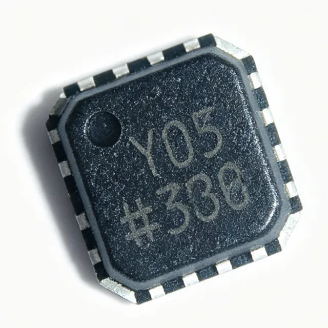
ADCLK905 - Ultrafast SiGe ECL Clock/Data Buffer | Analog Devices
部品番号: ADCLK905 ✓ 生産中| 数量 | 単価 | 小計 |
|---|---|---|
| 1 | $24.5455 | $24.55 |
| 10 | $17.7273 | $177.27 |
| 100 | $15.6818 | $1,568.18 |
| 500 | $15 | $7,500.00 |
| 1,000 | $14.3182 | $14,318.20 |
ADCLK905 概要
A clock/data buffer is a high-speed integrated circuit that receives a clock or data signal and re-drives it to one or more outputs with minimal added jitter and propagation delay. It is a critical component in signal distribution networks, ensuring signal integrity across multiple loads. The ADCLK905 belongs to the category of clock buffers, which are part of the broader clock and timing IC family. These devices are essential in systems where precise timing and low jitter are paramount, such as in high-speed ADCs, DACs, and serial data links.
Key features of the ADCLK905 include its 7.5 GHz toggle rate, which enables distribution of very high-frequency clocks, and its 60 fs random jitter, which preserves signal integrity in demanding applications. The 95 ps propagation delay ensures minimal latency, and the on-chip terminations simplify PCB layout by reducing external component count. The ECL output drivers provide full-swing signals compatible with ECL logic levels, and the extended industrial temperature range (-40°C to +125°C) supports harsh environments.
Technically, the ADCLK905 leverages the XFCB3 SiGe bipolar process, which offers high-speed performance with low power consumption. The device includes a differential input and output, allowing for flexible signal routing. The on-chip terminations at both input pins reduce reflections and improve signal quality. The LFCSP package with exposed pad provides excellent thermal performance, enabling reliable operation at high frequencies.
Typical applications include clock distribution for high-speed ADCs and DACs, data buffering in serial communication links, and signal conditioning in test and measurement equipment. The ADCLK905 is also suitable for use in RF and microwave systems where low jitter and high toggle rates are critical.
When designing with the ADCLK905, it is important to use high-quality PCB materials and proper termination techniques to maintain signal integrity at multi-gigahertz frequencies. The evaluation board uses high-quality dielectric material between layers to ensure optimal performance.
ドロップイン代替品: ADCLK905 — 同一パッケージでピン互換。PCBの作り直しが必要な異なるパッケージの部品は除外されています。
クイック比較ツール — 並列比較する代替部品を選択:
ADCLK907
📋 参考代替品(カタログ未掲載)
ADCLK925
📋 参考代替品(カタログ未掲載)
ADCLK905BCPZ-WP
📋 参考代替品(カタログ未掲載)
ADCLK905BCPZ-R7
📋 参考代替品(カタログ未掲載)
NB6L14MNG
📋 参考代替品(カタログ未掲載)
MC100EP16DTG
📋 参考代替品(カタログ未掲載)
ADCLK905 最大定格&電気的特性
| 機能 | Clock/Data Buffer |
| Number of Inputs | 1 |
| 出力数 | 1 |
| Toggle Rate | 7.5 GHz |
| Propagation Delay | 95 ps |
| Output Rise/Fall Time | 60 ps typical |
| Random Jitter | 60 fs |
| Logic Family | ECL |
| Input Termination | On-chip at both input pins |
| 動作温度範囲 | -40°C to +125°C |
| パッケージ | 16-lead LFCSP (VQFN) with exposed pad |
| 実装タイプ | Surface Mount |
| Process Technology | XFCB3 SiGe bipolar |
| RoHS ステータス | Compliant |
ADCLK905 ピン構成
| ピン 1 | CLK — Clock input (differential positive) |
| ピン 2 | CLKB — Clock input (differential negative) |
| ピン 3 | VCC — Positive supply |
| ピン 4 | VCC — Positive supply |
| ピン 5 | Q — Output (differential positive) |
| ピン 6 | QB — Output (differential negative) |
| ピン 7 | VCC — Positive supply |
| ピン 8 | VCC — Positive supply |
| ピン 9 | GND — Ground |
| ピン 10 | GND — Ground |
| ピン 11 | GND — Ground |
| ピン 12 | GND — Ground |
| ピン 13 | GND — Ground |
| ピン 14 | GND — Ground |
| ピン 15 | GND — Ground |
| ピン 16 | GND — Ground |
主な用途
ADCLK905 の用途: 6 件s: High-Speed ADC Clock Distribution, Data Buffering in Serial Links, RF and Microwave Signal Conditioning, Test and Measurement Equipment, Data Acquisition Systems, Communications Infrastructure.
High-Speed ADC Clock Distribution
The ADCLK905's 7.5 GHz toggle rate and 60 fs random jitter make it ideal for distributing low-jitter clocks to high-speed ADCs. Its 95 ps propagation delay ensures minimal latency, and the ECL outputs provide full-swing signals compatible with ADC clock inputs. The on-chip terminations simplify layout, reducing reflections and maintaining signal integrity at multi-gigahertz frequencies. This ensures optimal ADC dynamic performance, such as high SNR and SFDR, in applications like radar, communications, and test equipment.
おすすめ
Data Buffering in Serial Links
In high-speed serial communication links, the ADCLK905 buffers data signals with minimal added jitter, preserving signal integrity over long traces. Its 60 fs random jitter and 95 ps propagation delay ensure that data eye diagrams remain open, reducing bit error rates. The differential ECL outputs drive transmission lines effectively, and the on-chip terminations reduce external component count. This makes the ADCLK905 suitable for backplane distribution, optical module interfaces, and high-speed instrumentation.
おすすめ
RF and Microwave Signal Conditioning
The ADCLK905's ultra-low jitter and high toggle rate make it suitable for RF and microwave systems where clock quality directly impacts phase noise and system performance. It can distribute reference clocks to PLLs, mixers, and direct digital synthesizers with minimal degradation. The SiGe process provides high-speed operation with low power consumption, and the LFCSP package offers good thermal performance. This enables reliable operation in radar, satellite communication, and wireless infrastructure.
おすすめ
Test and Measurement Equipment
In oscilloscopes, spectrum analyzers, and signal generators, the ADCLK905 provides precise clock distribution to multiple measurement channels. Its 7.5 GHz toggle rate supports high-bandwidth sampling, while the 60 fs jitter ensures accurate timebase references. The extended temperature range (-40°C to +125°C) allows use in benchtop and field instruments. The on-chip terminations simplify PCB design, and the ECL outputs interface directly with high-speed comparators and ADCs.
おすすめ
Data Acquisition Systems
The ADCLK905 is used in data acquisition systems to distribute sampling clocks to multiple ADCs, ensuring synchronized and low-jitter sampling. Its 95 ps propagation delay minimizes skew between channels, and the 60 fs jitter preserves signal fidelity. The device's small LFCSP package and on-chip terminations reduce board space and component count, making it ideal for compact multi-channel systems. It supports high-speed data conversion in industrial, medical, and scientific applications.
おすすめ
Communications Infrastructure
In base stations, routers, and optical transport systems, the ADCLK905 buffers clock and data signals with minimal jitter, ensuring reliable high-speed data transmission. Its 7.5 GHz toggle rate supports emerging standards like 5G and 400G Ethernet. The ECL outputs drive long backplane traces, and the on-chip terminations reduce reflections. The extended temperature range and high reliability make it suitable for outdoor and industrial communications equipment.
おすすめ
おすすめ製品の概要
エンジニアリング参考データ: ADCLK905 — 比較、設計ガイダンス、コンプライアンス情報。
選定ガイド
代替品との比較
| パラメータ | この製品 | ADCLK907 | ADCLK925 | NB6L14MNG |
|---|---|---|---|---|
| Package | 16-lead LFCSP | 16-lead LFCSP | 16-lead LFCSP | 16-lead LFCSP |
| Brand | Analog Devices | Analog Devices | Analog Devices | onsemi |
| Toggle Rate | 7.5 GHz | 7.5 GHz | 7.5 GHz | 3 GHz |
| Propagation Delay | 95 ps | 95 ps | 95 ps | 400 ps |
| Random Jitter | 60 fs | 60 fs | 60 fs | 1 ps |
| Number of Outputs | 1 | 2 (dual buffer) | 2 (fan-out) | 4 |
| Logic Family | ECL | ECL | ECL | LVPECL |
| Operating Temperature Range | -40°C to +125°C | -40°C to +125°C | -40°C to +125°C | -40°C to +85°C |
主な差別化要因
- Ultra-low random jitter of 60 fs (vs NB6L14MNG)
- Higher toggle rate of 7.5 GHz (vs NB6L14MNG)
- Extended industrial temperature range (vs MC100EP16DTG)
設計ノート
For optimal performance at multi-gigahertz frequencies, use high-quality PCB materials such as Rogers or low-loss FR4. Ensure controlled impedance traces (50 ohm single-ended, 100 ohm differential) for all high-speed inputs and outputs. Place the ADCLK905 close to the load to minimize trace length and reduce signal degradation.
Decouple the VCC pins with 0.1 uF and 10 uF capacitors placed as close to the pins as possible. Use a low-noise power supply to avoid introducing jitter into the clock signal. The ADCLK905 requires a clean, stable supply voltage to maintain its low jitter performance.
Use differential routing for the input and output pairs to minimize common-mode noise. Keep the traces balanced and avoid vias where possible. The on-chip terminations simplify layout, but ensure the ground plane is continuous under the device to provide a low-inductance return path.
コンプライアンス情報
RoHS compliant per Analog Devices product page. Other compliance details not specified in provided data.







