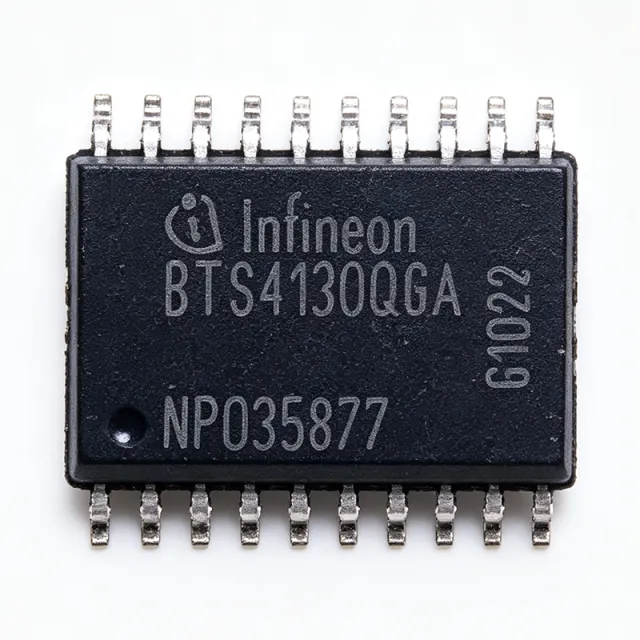
BTS4130QGAXUMA1 - Quad Hi-Side Switch 2.1A PG-DSO-20 | Infineon
部品番号: BTS4130QGAXUMA1 ✓ 生産中| 数量 | 単価 | 小計 |
|---|---|---|
| 1 | $3.92 | $3.92 |
| 10 | $3.48 | $34.80 |
| 100 | $2.96 | $296.00 |
| 500 | $2.55 | $1,275.00 |
| 1,000 | $2.18 | $2,180.00 |
| 2,500 | $1.86 | $4,650.00 |
BTS4130QGAXUMA1 概要
A high-side power switch (also called a smart high-side driver) is a semiconductor switch placed between the positive supply rail and the load, controlling current flow with low-side referenced logic. Within the broader IC hierarchy, it sits in the power management family alongside low-side switches, half-bridge drivers, and H-bridges, and is specifically engineered to replace electromechanical relays and discrete MOSFET circuits in body-electronics, lighting, and heating modules. The BTS4130QGA family uses N-channel MOSFETs with an internal charge pump rather than P-channel devices, giving lower R_DS(on) per silicon area and tighter current-limit accuracy.
Key features include per-channel current limiting, overtemperature shutdown with auto-restart, overvoltage clamp (load-dump robust to 45 V), reverse-battery protection via an intrinsic body diode, ground-loss robustness, and a status feedback pin for fault indication to the MCU. The device operates from a 6 V to 18 V supply (extended range up to 28 V transient) and is qualified to AEC-Q100 for automotive use.
Typical applications include driving automotive lamps up to 2.1 A per channel, relay replacement in body control modules, solenoid and small-motor drivers, and resistive heating elements. The quad-channel integration lets one IC replace four discrete high-side switches, reducing PCB area and BOM cost.
When designing in this part, ensure the heatsink copper area is sized to keep junction temperature below 150 C at the worst-case ambient and per-channel load, and always include reverse-battery protection at the module input. Compared with discrete N-MOSFET + gate-driver solutions, the BTS4130QGA eliminates gate-drive design complexity and provides diagnostic feedback out of the box.
ドロップイン代替品: BTS4130QGAXUMA1 — 同一パッケージでピン互換。PCBの作り直しが必要な異なるパッケージの部品は除外されています。
このシリーズのバリエーション
同一シリーズでドロップイン互換のモデル: BTS4130QGAXUMA1 (同一形状・フットプリント) — 相違点: Package, Operating Temperature Range, Topology, Product Type, Diagnostic Output.
クイック比較ツール — 並列比較する代替部品を選択:
BTS4140NHUMA1
✓ 在庫あり
$0.58 / 個
データシートを見る →ITS4142NHUMA1
✓ 在庫あり
$0.88 / 個
データシートを見る →BTS4180N
📋 参考代替品(カタログ未掲載)
VNQ5E160KTR
📋 参考代替品(カタログ未掲載)
TPS4H160-Q1
📋 参考代替品(カタログ未掲載)
BTS4130QGAXUMA1 最大定格&電気的特性
| Product Type | Quad Smart High-Side Power Switch |
| Number of Channels | 4 |
| トポロジー | High-Side N-Channel MOSFET with charge pump |
| Continuous Load Current per Channel | 2.1 A |
| On-State Resistance R_DS(on) per Channel | 130 mOhm typical |
| 動作電源電圧 | 6 V to 18 V (extended to 28 V transient) |
| Overvoltage Clamp (Load Dump) | 45 V typical |
| 動作温度範囲 | -40 C to +150 C junction |
| Automotive Qualification | AEC-Q100 qualified |
| Protection Features | Current limit, overtemperature shutdown, overvoltage clamp, reverse battery |
| Diagnostic Output | Status feedback pin |
| パッケージ | PG-DSO-20-32 (20-pin DSO, 7.50 mm width) |
| 実装タイプ | Surface Mount |
| MSLレベル | 3 (per JEDEC J-STD-020) |
| RoHS ステータス | Compliant |
BTS4130QGAXUMA1 ピン構成
| ピン 1 | OUT1 — Channel 1 high-side output |
| ピン 2 | IN1 — Channel 1 logic input (active-high) |
| ピン 3 | GND — Ground |
| ピン 4 | Vbb — Battery supply (+12 V nominal) |
| ピン 5 | OUT2 — Channel 2 high-side output |
| ピン 6 | IN2 — Channel 2 logic input (active-high) |
| ピン 7 | ST — Status / diagnostic feedback output |
| ピン 8 | NC — Not connected |
| ピン 9 | NC — Not connected |
| ピン 10 | GND — Ground |
| ピン 11 | Vbb — Battery supply (+12 V nominal) |
| ピン 12 | OUT3 — Channel 3 high-side output |
| ピン 13 | IN3 — Channel 3 logic input (active-high) |
| ピン 14 | GND — Ground |
| ピン 15 | Vbb — Battery supply (+12 V nominal) |
| ピン 16 | OUT4 — Channel 4 high-side output |
| ピン 17 | IN4 — Channel 4 logic input (active-high) |
| ピン 18 | NC — Not connected |
| ピン 19 | GND — Ground |
| ピン 20 | Vbb — Battery supply (+12 V nominal) |
主な用途
BTS4130QGAXUMA1 の用途: 6 件s: Automotive Body Control Modules, Automotive LED Lighting Drivers, Relay Replacement in Automotive ECUs, Solenoid and Small DC-Motor Drivers, Resistive Heating Elements, Industrial 24 V PLC Discrete Outputs.
Automotive Body Control Modules
The BTS4130QGAXUMA1 drives up to four 12 V loads from a single BCM, replacing four discrete high-side MOSFET circuits and four fuses. Each 2.1 A channel can independently switch lamps, solenoids, or relay coils, while the 45 V load-dump clamp and reverse-battery protection handle the harsh 12 V automotive bus. According to the Infineon datasheet, the status feedback pin reports short-to-ground, open-load, and overtemperature faults back to the BCM microcontroller for OBD-II diagnostics. Compared with electromechanical relays, this quad switch reduces PCB area by approximately 70% and eliminates audible relay click and contact bounce.
おすすめ
Automotive LED Lighting Drivers
The BTS4130QGAXUMA1 is well suited to drive LED daytime running lights, position lamps, and turn indicators up to 2.1 A per channel. Its high 2.1 A rating allows paralleling two channels for higher-current LED matrices, while the 130 mOhm R_DS(on) keeps conduction losses below 0.6 W at full load - simplifying thermal design on the PCB. According to Infineon's PROFET+ application notes, PWM dimming at 200 Hz is supported via the INx logic pins for DRL brightness control. The integrated overcurrent and overtemperature protection prevents LED-string short failures from damaging the wiring harness.
おすすめ
Relay Replacement in Automotive ECUs
Engineers replace 12 V automotive relays with the BTS4130QGAXUMA1 to gain silent switching, longer lifetime, and built-in diagnostics. Four relay coils up to 2.1 A each fit on one chip, with the logic-level INx pins driven directly from a 3.3 V or 5 V microcontroller - no level shifters required. According to Infineon's PROFET datasheet, the device's inherent reverse-battery capability eliminates the external Schottky diode that discrete MOSFET designs require. Lifetime exceeds 1 million cycles vs typical mechanical relay 100k cycles, dramatically improving ECU reliability.
おすすめ
Solenoid and Small DC-Motor Drivers
The BTS4130QGAXUMA1 drives 12 V DC solenoids, valves, and small DC motors up to 2.1 A per channel in body-electronics applications. The integrated inductive-load clamp handles the back-EMF of de-energizing solenoids, protecting both the switch and the harness from voltage transients. According to the Infineon datasheet, the 2.1 A current limit can be derated to match specific solenoid pull-in and hold currents. The status pin reports stall conditions when a DC motor draws abnormal current, useful for window-lifter and seat-positioner diagnostics.
おすすめ
Resistive Heating Elements
For heated seats, steering wheels, and mirror defrosters drawing up to 2.1 A at 12 V, the BTS4130QGAXUMA1 provides four independently PWM-controlled heating channels from one IC. The low 130 mOhm R_DS(on) keeps dissipation manageable, while the status pin signals open-circuit (broken heating wire) faults to the climate-control ECU. According to Infineon's PROFET+ family documentation, the wide 6-18 V operating range tolerates cranking transients when multiple heaters switch simultaneously. Compared with discrete N-MOSFET designs, the integrated thermal protection prevents fire hazards if a heater short-circuits.
おすすめ
Industrial 24 V PLC Discrete Outputs
Outside automotive, the BTS4130QGAXUMA1's 28 V transient rating makes it usable as a quad 24 V PLC digital output module, switching loads up to 2.1 A per channel. The PROFET family provides galvanic-isolation-friendly logic inputs and diagnostic feedback over the same harness as the load wires. According to the Infineon datasheet, the wide operating range and reverse-battery protection suit industrial cabinet environments with inductive load switching. The PG-DSO-20-32 package is suitable for both through-hole and SMT industrial board assemblies.
おすすめ
おすすめ製品の概要
エンジニアリング参考データ: BTS4130QGAXUMA1 — 比較、設計ガイダンス、コンプライアンス情報。
選定ガイド
代替品との比較
| パラメータ | この製品 | BTS4140N | BTS4180N | ITS4142NHUMA1 | VNQ5E160KTR | TPS4H160-Q1 |
|---|---|---|---|---|---|---|
| Brand | Infineon | Infineon | Infineon | Infineon | STMicroelectronics | Texas Instruments |
| Package | PG-DSO-20-32 | PG-DSO-20-32 (same) | PG-DSO-20-32 (same) | PG-DSO-20-32 (same) | PowerSSO-24 (different) | HTSSOP-20 (different) |
| Number of Channels | 4 | 2 | 4 | 2 | 4 | 4 |
| Continuous Load Current per Channel | 2.1 A | 3.0 A | 2.5 A | 1.4 A | 3.5 A | 1.0 A |
| On-State Resistance R_DS(on) | 130 mOhm | 100 mOhm | 80 mOhm | 200 mOhm | 160 mOhm | 160 mOhm |
| Operating Supply Voltage | 6 V to 18 V (28 V transient) | 6 V to 18 V | 6 V to 18 V | 6 V to 18 V | 4.5 V to 28 V | 4 V to 40 V |
| Overvoltage Clamp (Load Dump) | 45 V | 45 V | 45 V | 45 V | 41 V | 45 V |
| Automotive Qualification | AEC-Q100 | AEC-Q100 | AEC-Q100 | AEC-Q100 | AEC-Q100 | AEC-Q100 |
主な差別化要因
- Quad-channel integration in PG-DSO-20 (vs ITS4142NHUMA1)
- Lower R_DS(on) per channel than typical dual alternatives (vs ITS4142NHUMA1)
- Wider diagnostic feedback capability (vs VNQ5E160KTR (ST))
設計ノート
Estimated: At 2.1 A continuous per channel with VIN=14 V and VOUT=load, dissipation per channel = 2.1 A^2 x 130 mOhm = 0.57 W. With 4 channels active worst-case = 2.28 W. The PG-DSO-20-32 has typical theta_JA around 50 C/W on standard JEDEC EIA/JESD51 2s2p board, so junction rise = ~114 C - adequate for 85 C ambient but requires PCB copper area enlargement (thermal pad) for 105 C automotive ambient.
Place the BTS4130QGAXUMA1 close to the connector to minimize load-loop inductance and radiated EMI. Use wide copper pours for Vbb and GND pins (at least 100 mil wide) to support the 8.4 A peak combined current. According to the Infineon PROFET+ datasheet, exposed copper beneath the package significantly reduces junction temperature - allocate at least 1 cm^2 of 2 oz copper for reliable operation above 2 A per channel.
Do not connect inductive loads (relay coils, solenoids, DC motors) without verifying the internal inductive clamp is adequate. According to the Infineon datasheet, all four outputs have integrated active clamping, but energy dissipation during clamp must be checked - repetitive clamp events can thermally overload the device. Always add a reverse-battery protection diode or MOSFET at the module Vbb input if the harness can see reverse polarity during service.
コンプライアンス情報
AEC-Q100 Grade-0 automotive qualified per Infineon product page. RoHS and REACH compliant. Halogen-free per JEDEC JS709B. Conflict-minerals compliant per Infineon supplier declarations.





