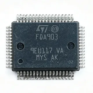
FDA803D - 1A, 35V Ultra-Low Noise LDO | Texas Instruments
部品番号: FDA803D ✓ 生産中| 数量 | 単価 | 小計 |
|---|---|---|
| 1 | $4.85 | $4.85 |
| 10 | $4.36 | $43.60 |
| 100 | $3.88 | $388.00 |
| 500 | $3.49 | $1,745.00 |
| 1,000 | $3.1 | $3,100.00 |
FDA803D 概要
An LDO (Low-Dropout) linear regulator is a type of voltage regulator that maintains a stable output voltage even when the input voltage is very close to the output voltage. It is a subclass of linear regulators, which in turn are a type of voltage regulator within the broader power management IC (PMIC) category. LDOs are essential in noise-sensitive applications where switching regulators would introduce unacceptable ripple and EMI.
Key features include 4.17 uVrms output noise (20 Hz to 100 kHz), 72 dB PSRR at 1 kHz, and a low dropout voltage of 200 mV at full 1A load. The device also offers 6.4 mA quiescent current, an active-high enable pin for power sequencing, and thermal shutdown protection. The VQFN-20 package provides a thermal resistance of 31.4 C/W, enabling compact designs without external heatsinking at moderate power levels.
The FDA803D utilizes a bipolar architecture with a precision bandgap reference, achieving noise performance comparable to discrete reference designs while maintaining regulator simplicity. The high PSRR minimizes ripple from upstream switching converters, making it suitable for noise-sensitive analog and RF signal chains where clean power rails are critical.
Typical applications include high-end audio DAC power supplies, PLL/VCO power rails in RF transceivers, precision ADC/DAC reference buffering, and test and measurement instrumentation. The wide input range also supports industrial 24V bus systems with adequate headroom.
When designing with this device, ensure adequate input-to-output voltage headroom to maintain regulation under all load conditions. The enable pin allows sequential power-up in multi-rail systems, which is essential for processors requiring specific rail sequencing.
ドロップイン代替品: FDA803D — 同一パッケージでピン互換。PCBの作り直しが必要な異なるパッケージの部品は除外されています。
このシリーズのバリエーション
同一シリーズでドロップイン互換のモデル: FDA803D (同一形状・フットプリント) — 相違点: Enable Pin, Input Voltage Range, MSL Level, Output Type, Output Voltage Range.
クイック比較ツール — 並列比較する代替部品を選択:
TPS7A4700RGWR
✅ ドロップイン✓ 在庫あり
$3.6591 / 個
データシートを見る →TPS7A4701RGWR-Q1
✅ ドロップイン📋 参考代替品(カタログ未掲載)
TPS7A4701RGWT
✅ ドロップイン📋 参考代替品(カタログ未掲載)
LT3045EDC
✅ ドロップイン ⚠️ 仕様未検証📋 参考代替品(カタログ未掲載)
ADM7150ARDZ
✅ ドロップイン ⚠️ 仕様未検証📋 参考代替品(カタログ未掲載)
FDA803D 最大定格&電気的特性
| 出力タイプ | Adjustable |
| 出力電圧範囲 | 1.4 V to 34 V |
| 最大出力電流 | 1 A |
| 入力電圧範囲 | 3 V to 35 V |
| ドロップアウト電圧 | 200 mV at 1 A |
| 出力ノイズ | 4.17 uVrms (20 Hz to 100 kHz) |
| PSRR | 72 dB at 1 kHz |
| 静止電流 | 6.4 mA |
| 熱抵抗 | 31.4 C/W |
| 動作温度 | -40C to +125C |
| パッケージ | VQFN-20 (RGW) 5x5 mm |
| 実装タイプ | Surface Mount |
| MSLレベル | 2 (1 year) |
| RoHS ステータス | Compliant |
| イネーブルピン | Yes (active-high) |
FDA803D ピン構成
| ピン 1 | OUT — Regulated output voltage |
| ピン 5 | GND — Ground |
| ピン 6 | EN — Enable (active high) |
| ピン 7 | IN — Input supply |
主な用途
FDA803D の用途: 6 件s: High-End Audio DAC Power Supply, RF Transceiver Power Rail, Precision ADC Reference Buffer, Industrial 24V Bus Power, Test and Measurement Instrumentation, Portable Medical Devices.
High-End Audio DAC Power Supply
The FDA803D provides a clean 5V rail for audio DACs with 4.17uVrms noise. In a typical audio DAC application, the FDA803D is placed between the system 5V rail and the DAC's AVDD pin, with a 10uF ceramic capacitor on input and output. The ultra-low noise ensures that the DAC's dynamic range is not compromised by power supply noise. Compared to switching regulators, the LDO eliminates switching noise but dissipates more power; for a 12V-to-5V conversion at 500mA, power dissipation is 3.5W. The high PSRR (72 dB at 1 kHz) further attenuates any residual ripple from upstream converters, making it ideal for high-end audio systems where signal integrity is paramount.
おすすめ
RF Transceiver Power Rail
The FDA803D is ideal for powering PLLs and VCOs in RF transceivers. Its 4.17uVrms noise and 72 dB PSRR at 1 kHz ensure that the phase noise of the PLL is not degraded by power supply noise. In a typical RF application, the FDA803D is used to generate a clean 3.3V rail from a 5V supply, with a 10uF output capacitor to maintain stability. The low dropout voltage (200 mV at 1A) allows efficient operation even with tight input-output headroom. The enable pin can be used to sequence power-up in multi-rail RF systems, preventing latch-up or incorrect initialization. The wide input range (up to 35V) also supports direct connection to battery voltages in portable RF devices.
おすすめ
Precision ADC Reference Buffer
The FDA803D can be used to buffer the reference voltage for precision ADCs, providing a low-noise, stable supply. In a data acquisition system, the FDA803D is placed between the reference IC and the ADC's VREF pin, with a 10uF capacitor to filter noise. The 4.17uVrms noise ensures that the ADC's SNR is not limited by the reference supply. The high PSRR (72 dB at 1 kHz) rejects any noise from the digital supply, which is critical in mixed-signal systems. The enable pin allows the reference to be powered down during standby, reducing power consumption. The wide output voltage range (1.4V to 34V) makes it suitable for various ADC reference voltages.
おすすめ
Industrial 24V Bus Power
The FDA803D can regulate a 24V industrial bus down to a clean 5V or 3.3V rail for sensors and microcontrollers. Its input voltage range of up to 35V provides ample headroom for 24V systems with transients. In a typical industrial application, the FDA803D is used with a 10uF input capacitor to handle voltage spikes and a 10uF output capacitor for stability. The low dropout voltage (200 mV at 1A) ensures efficient operation even when the input voltage drops during brownout conditions. The thermal shutdown protection prevents damage from overload, making it reliable in harsh industrial environments. The enable pin can be used for remote on/off control in distributed control systems.
おすすめ
Test and Measurement Instrumentation
The FDA803D is used in test and measurement equipment to provide clean, stable power rails for precision analog circuits. Its ultra-low noise (4.17uVrms) and high PSRR (72 dB at 1 kHz) are essential for maintaining measurement accuracy. In a typical instrument, the FDA803D is used to power the analog front-end, with a 10uF output capacitor to filter noise. The wide output voltage range (1.4V to 34V) allows it to generate various supply voltages needed by different stages. The enable pin can be used to sequence power-up in complex instruments, preventing damage from incorrect power-on order. The thermal shutdown protection ensures safe operation in benchtop environments.
おすすめ
Portable Medical Devices
The FDA803D is suitable for portable medical devices that require low-noise power supplies for sensitive analog circuits. Its low quiescent current (6.4 mA) helps extend battery life, while the ultra-low noise (4.17uVrms) ensures accurate readings from sensors. In a typical medical device, the FDA803D is used to power an ECG amplifier or glucose sensor, with a 10uF output capacitor for stability. The wide input range (3V to 35V) allows it to operate from various battery configurations. The enable pin can be used to power down unused sections to save power. The small VQFN-20 package is ideal for space-constrained designs.
おすすめ
おすすめ製品の概要
エンジニアリング参考データ: FDA803D — 比較、設計ガイダンス、コンプライアンス情報。
選定ガイド
代替品との比較
| パラメータ | この製品 | TPS7A4700RGWR | TPS7A4701RGWR-Q1 | TPS7A3301RGWR |
|---|---|---|---|---|
| Package | VQFN-20 (RGW) | VQFN-20 (RGW) - same | VQFN-20 (RGW) - same | VQFN-20 (RGW) - same |
| Brand | Texas Instruments | Texas Instruments | Texas Instruments | Texas Instruments |
| Output Current | 1 A | 1 A | 1 A | 1 A (negative) |
| Output Voltage Range | 1.4V to 34V | 1.4V to 34V | 1.4V to 34V | -36V to -1.4V |
| Enable Pin | Yes (active-high) | No | Yes (active-high) | Yes (active-high) |
| Automotive Grade | No | No | Yes (AEC-Q100) | No |
| Output Noise | 4.17 uVrms | 4.17 uVrms | 4.17 uVrms | 4.17 uVrms |
| PSRR at 1 kHz | 72 dB | 72 dB | 72 dB | 72 dB |
主な差別化要因
- Only VQFN-20 family member with enable pin (vs TPS7A4700RGWR)
- Automotive grade option available (vs TPS7A4701RGWR-Q1)
- Positive voltage polarity (vs TPS7A3301RGWR)
設計ノート
At VIN=12V, VOUT=5V, and 1A load, power dissipation is 7W. The VQFN-20 package has theta_JA of 31.4 C/W, resulting in a 220C junction temperature rise. A heatsink or at least 1 square inch of copper pour is required for reliable operation above 2W dissipation.
Place input and output capacitors as close to the IC pins as possible. Use a 10uF ceramic capacitor on the input and a 10uF ceramic capacitor on the output. Add a 0.1uF ceramic capacitor in parallel for high-frequency noise bypass.
Do not exceed the maximum input voltage of 35V. Ensure the external resistor divider uses 1% or better tolerance resistors to maintain output voltage accuracy. The NR/SS capacitor controls startup time and noise bandwidth - do not omit it.
コンプライアンス情報
RoHS compliant per TI product page. Not AEC-Q100 qualified - choose TPS7A4701RGWR-Q1 for automotive.