Texas Instruments

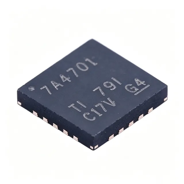
TPS7A4701RGWR - 1A, 35V Ultra-Low Noise LDO | Texas Instruments

部品番号: TPS7A4701RGWR ✓ 生産中
在庫あり 1〜3営業日以内に発送
1.4 V to 34 V Vdss 1 A Id 31.4 C/W Rds(on) VQFN-20 (RGW) 5x5 mm Package
開始価格 $3.2467 USD / 個
MOQ: 1 |
価格更新日: 2026-09-02
ボリューム価格
数量 単価 小計
1 $3.2467 $3.25
ℹ️ すべての価格はUSDです

TPS7A4701RGWR 概要

The Texas Instruments TPS7A4701RGWR is an ultra-low-noise, high-PSRR LDO linear regulator delivering up to 1A output current in a 20-pin VQFN (RGW) package with exposed thermal pad. It features an adjustable output voltage range of 1.4V to 34V and supports input voltages from 3V to 35V.

Key features include 4.17 uVrms output noise (20 Hz to 100 kHz), 72 dB PSRR at 1 kHz, and a low dropout voltage of 200 mV at full 1A load. The device also offers 6.4 mA quiescent current, an active-high enable pin for power sequencing, and thermal shutdown protection. The VQFN-20 package provides a thermal resistance of 31.4 C/W, enabling compact designs without external heatsinking at moderate power levels.

The TPS7A4701 utilizes a bipolar architecture with a precision bandgap reference, achieving noise performance comparable to discrete reference designs while maintaining regulator simplicity. The high PSRR minimizes ripple from upstream switching converters, making it suitable for noise-sensitive analog and RF signal chains where clean power rails are critical.

Typical applications include high-end audio DAC power supplies, PLL/VCO power rails in RF transceivers, precision ADC/DAC reference buffering, and test and measurement instrumentation. The wide input range also supports industrial 24V bus systems with adequate headroom.

When designing with this device, ensure adequate input-to-output voltage headroom to maintain regulation under all load conditions. The enable pin allows sequential power-up in multi-rail systems, which is essential for processors requiring specific rail sequencing.

ドロップイン代替品: TPS7A4701RGWR — 同一パッケージでピン互換。PCBの作り直しが必要な異なるパッケージの部品は除外されています。

このシリーズのバリエーション

同一シリーズでドロップイン互換のモデル: TPS7A4701RGWR (同一形状・フットプリント) — 相違点: Input Voltage Range, Output Voltage Range, Package, RoHS Status.

Intel
Input Voltage Range: 2.2 V to 6 V
Output Voltage Range: 0.8 V to 5 V (adjustable)
Package: 10-DFN (3x3 mm), Pb-Free
比較対象 TPS7A4701RGWR →

クイック比較ツール — 並列比較する代替部品を選択:

TPS7A4700RGWR

Texas Instruments
Positive, adjustable (ANY-OUT programmable) · 1.4 V to 20.5 V (ANY-OUT via PCB layout) · 1 A · 3 V to 36 V · 4.17 uVRMS (20 Hz to 100 kHz)

✓ 在庫あり

$3.6591 / 個

データシートを見る →

TPS7A4701RGWR-Q1

same die/package, AEC-Q100 automotive grade

📋 参考代替品(カタログ未掲載)

TPS7A4701RGWT

same die, tape and reel packaging variant

📋 参考代替品(カタログ未掲載)

TPS7A4701RGWR 最大定格&電気的特性

出力タイプ Adjustable
出力電圧範囲 1.4 V to 34 V
最大出力電流 1 A
入力電圧範囲 3 V to 35 V
ドロップアウト電圧 200 mV at 1 A
出力ノイズ 4.17 uVrms (20 Hz to 100 kHz)
PSRR 72 dB at 1 kHz
静止電流 6.4 mA
熱抵抗 31.4 C/W
動作温度 -40C to +125C
パッケージ VQFN-20 (RGW) 5x5 mm
実装タイプ Surface Mount
MSLレベル 2 (1 year)
RoHS ステータス Compliant
イネーブルピン Yes (active-high)

TPS7A4701RGWR ピン構成

VQFN-20 Package Pinout Diagram VQFN-20 (RGW) 5x5mm, P0.5mm, exposed pad 3.3x3.3mm, JEDEC MO-220. Pin 1 top-left, numbered CCW. EP Exposed Pad 1 2 3 4 5 6 7 8 9 10 11 12 13 14 15 16 17 18 19 20 VQFN-20 (5x5mm)
ピン 1 OUT — Regulated output voltage
ピン 2 OUT — Regulated output voltage
ピン 3 OUT — Regulated output voltage
ピン 4 OUT — Regulated output voltage
ピン 5 GND — Ground
ピン 6 EN — Enable (active high)
ピン 7 IN — Input supply
ピン 8 IN — Input supply
ピン 9 IN — Input supply
ピン 10 IN — Input supply
ピン 11 NR/SS — Noise reduction/soft-start
ピン 12 FB — Feedback
ピン 13 GND — Ground
ピン 14 GND — Ground
ピン 15 GND — Ground
ピン 16 GND — Ground
ピン 17 GND — Ground
ピン 18 GND — Ground
ピン 19 GND — Ground
ピン 20 GND — Ground

主な用途

TPS7A4701RGWR の用途: 6 件s: High-End Audio DAC Power Supply, RF Transceiver Power Supply, Precision ADC Reference Buffer, Test and Measurement Instrumentation, Industrial 24V Bus Systems, Portable Medical Devices.

🎧

High-End Audio DAC Power Supply

Provides clean 5V rail for audio DACs with 4.17uVrms noise.

🌐

RF Transceiver Power Supply

Supplies low-noise power to PLL/VCO circuits in RF transceivers.

🔧

Precision ADC Reference Buffer

Buffers reference voltage for precision ADCs with low noise.

🔧

Test and Measurement Instrumentation

Provides clean power rails for sensitive measurement circuits.

🏭

Industrial 24V Bus Systems

Regulates 24V industrial bus down to low-noise rails for sensors and controllers.

💊

Portable Medical Devices

Provides low-noise power for battery-operated medical monitoring equipment.

おすすめ製品の概要

PCM1794A DAC requiring low-noise power 使用用途: High-End Audio DAC Power Supply OPA1612 I/V converter op-amp 使用用途: High-End Audio DAC Power Supply LMX2594 PLL synthesizer needing clean supply 使用用途: RF Transceiver Power Supply TRF37B32 RF amplifier 使用用途: RF Transceiver Power Supply ADS8881 18-bit SAR ADC 使用用途: Precision ADC Reference Buffer REF5025 Voltage reference 使用用途: Precision ADC Reference Buffer ADS1262 Texas Instruments 使用用途: Test and Measurement Instrumentation OPA2188 Zero-drift op-amp 使用用途: Test and Measurement Instrumentation MSP430FR5969 Low-power MCU 使用用途: Industrial 24V Bus Systems ISO7741 Digital isolator 使用用途: Industrial 24V Bus Systems ADS1292R ECG front-end 使用用途: Portable Medical Devices MSP432P401R MCU 使用用途: Portable Medical Devices
What is the output voltage range of TPS7A4701?
The TPS7A4701 adjustable version outputs from 1.4V to 34V using external resistor dividers. According to TI datasheet SBOS708B, the output is set by two external resistors with the formula VOUT = 1.4V * (1 + R1/R2).
Does TPS7A4701 require a heatsink at 1A output?
At VIN=12V, VOUT=5V, and 1A load, the TPS7A4701 dissipates approximately 7W of power. With a thermal resistance of 31.4 C/W (theta_JA), the junction temperature would rise 220C above ambient. A heatsink or substantial copper pour (at least 1 square inch) is required for reliable operation above 2-3W dissipation.
What is the difference between TPS7A4701 and TPS7A4700?
The TPS7A4701 includes an active-high enable pin for power sequencing, while the TPS7A4700 does not have an enable pin. Both share identical noise (4.17 uVrms) and PSRR (72 dB at 1 kHz) specifications and the same VQFN-20 (RGW) package, making them drop-in replacements.
What is the output noise of TPS7A4701?
The TPS7A4701 has an output noise of 4.17 uVrms over the 20 Hz to 100 kHz bandwidth. This makes it suitable for noise-sensitive applications such as audio DACs, RF synthesizers, and precision ADC references.
Can TPS7A4701 be used for audio applications?
Yes, the TPS7A4701 is ideal for audio DAC power supplies due to its 4.17 uVrms ultra-low noise and 72 dB PSRR at 1 kHz. These specifications ensure clean power rails that do not introduce audible noise or interference into the audio signal path.
What is the input voltage range of TPS7A4701?
The TPS7A4701 operates with an input voltage range from 3V to 35V. This wide range allows it to be used in various applications, including industrial 24V bus systems and battery-powered devices.
What is the dropout voltage of TPS7A4701?
The TPS7A4701 has a low dropout voltage of 200 mV at full 1A load. This low dropout allows efficient regulation even when the input voltage is close to the output voltage, reducing power dissipation.
Is TPS7A4701 available in automotive grade?
The standard TPS7A4701RGWR is not AEC-Q100 qualified. However, the TPS7A4701RGWR-Q1 variant is AEC-Q100 qualified for automotive applications, sharing the same VQFN-20 (RGW) package and pinout.
What is the quiescent current of TPS7A4701?
The TPS7A4701 has a quiescent current of 6.4 mA. This relatively low quiescent current helps maintain efficiency in battery-powered applications while providing high performance.
What is the PSRR of TPS7A4701?
The TPS7A4701 achieves a PSRR of 72 dB at 1 kHz. This high power supply rejection ratio minimizes ripple from upstream switching converters, making it ideal for noise-sensitive analog and RF circuits.
What is the package of TPS7A4701?
The TPS7A4701 is available in a 20-pin VQFN (RGW) package measuring 5x5 mm with an exposed thermal pad. This compact package is suitable for space-constrained designs and provides good thermal performance.
What is the operating temperature range of TPS7A4701?
The TPS7A4701 operates over a temperature range of -40C to +125C. This wide range makes it suitable for industrial and automotive environments where extreme temperatures are common.
Does TPS7A4701 have thermal shutdown protection?
Yes, the TPS7A4701 includes thermal shutdown protection. This feature prevents damage from overheating by shutting down the regulator when the junction temperature exceeds safe limits.
What is the MSL level of TPS7A4701?
The TPS7A4701 has an MSL (Moisture Sensitivity Level) of 2, with a floor life of 1 year. This indicates the component can be stored for up to one year before soldering, provided it is kept in a dry environment.
Is TPS7A4701 RoHS compliant?
Yes, the TPS7A4701 is RoHS compliant. This ensures it meets the European Union's restrictions on hazardous substances, making it suitable for use in consumer and industrial products.

エンジニアリング参考データ: TPS7A4701RGWR — 比較、設計ガイダンス、コンプライアンス情報。

選定ガイド

Choose TPS7A4701RGWR when you need a positive-output ultra-low-noise LDO with enable pin for power sequencing in industrial or consumer applications. Choose TPS7A4700RGWR if you do not need the enable pin (slight cost savings, same package). Choose TPS7A4701RGWR-Q1 for automotive applications requiring AEC-Q100 qualification. Choose TPS7A4701RGWT if you prefer a different tape and reel ordering option, but note it is electrically identical. All parts share the same VQFN-20 (RGW) package footprint, enabling PCB layout reuse across variants.

代替品との比較

パラメータ この製品 TPS7A4700RGWR TPS7A4701RGWR-Q1 TPS7A4701RGWT
Package VQFN-20 (RGW) VQFN-20 (RGW) - same VQFN-20 (RGW) - same VQFN-20 (RGW) - same
Output Current 1 A 1 A 1 A 1 A
Output Voltage Range 1.4V to 34V 1.4V to 34V 1.4V to 34V 1.4V to 34V
Enable Pin Yes (active-high) No Yes (active-high) Yes (active-high)
Automotive Grade No No Yes (AEC-Q100) No
Output Noise 4.17 uVrms 4.17 uVrms 4.17 uVrms 4.17 uVrms
PSRR at 1 kHz 72 dB 72 dB 72 dB 72 dB
Quiescent Current 6.4 mA 6.4 mA 6.4 mA 6.4 mA

主な差別化要因

  • Only VQFN-20 family member with enable pin (vs TPS7A4700RGWR)
  • Automotive grade option available (vs TPS7A4701RGWR-Q1)
  • Tape and reel packaging variant (vs TPS7A4701RGWT)

設計ノート

At VIN=12V, VOUT=5V, and 1A load, power dissipation is 7W. The VQFN-20 package has theta_JA of 31.4 C/W, resulting in a 220C junction temperature rise. A heatsink or at least 1 square inch of copper pour is required for reliable operation above 2W dissipation.

Place input and output capacitors as close to the IC pins as possible. Use a 10uF ceramic capacitor on the input and a 10uF ceramic capacitor on the output. Add a 0.1uF ceramic capacitor in parallel for high-frequency noise bypass.

Do not exceed the maximum input voltage of 35V. Ensure the external resistor divider uses 1% or better tolerance resistors to maintain output voltage accuracy. The NR/SS capacitor controls startup time and noise bandwidth - do not omit it.

コンプライアンス情報

RoHS
Compliant
REACH
Compliant
AEC-Q100
鉛フリー
ハロゲンフリー
紛争鉱物
Compliant

RoHS compliant per TI product page. Not AEC-Q100 qualified - choose TPS7A4701RGWR-Q1 for automotive.

データ検証日: 2026-08-17 — データはXAIPARTの部品エンジニアリングチームによって検証・管理されています

関連検索

TPS7A4701RGWR TPS7A4701 datasheet Texas Instruments TPS7A4701 ultra low noise LDO 1A 35V VQFN-20 LDO regulator TPS7A4701 audio DAC power supply TPS7A4701 vs TPS7A4700 TPS7A4701 drop-in replacement TPS7A4701RGWR buy price what is the output noise of TPS7A4701 TPS7A4701 pinout VQFN-20 low noise voltage regulator RF application

関連部品&用語

Texas Instruments TPS7A4701 TPS7A4701RGWR TPS7A4700RGWR TPS7A4701RGWR-Q1 TPS7A4701RGWT LDO linear regulator PSRR VQFN-20 RoHS AEC-Q100 audio DAC RF power supply bandgap reference thermal shutdown enable pin
関連技術ガイド
TPS7A4701RGWR:TI の 1A、35V 超低ノイズ LDO レギュレータ完全ガイド
TPS7A4701RGWR:TI の 1A 超低ノイズ LDO、4.17 uVrms ノイズ、72 dB PSRR、3~35V 入力、VQFN-20。在庫あり、2026-09-02 時点で $3.2467。
6 分で読了
TPS7A4700RGWR:36V 1A 超低ノイズ LDO — エンジニア向け完全ガイド、仕様、代替品
TPS7A4700RGWR:TI 36V 入力、1A LDO、4.17 µVRMS ノイズ、ANY-OUT プログラミング 1.4~20.5V、VQFN-20。XAIPART にて在庫あり。
8 分で読了
クイック見積RFQ
詳細をすべてご記入ください — 営業チームが24時間以内にご返信いたします
部品番号 メーカー パッケージ QTY 目標価格 小計
合計: $0.00 USD
✓
見積を送信しました!

24時間以内にメールでご返信いたします

1
RFQ送信済み
2
見積受領
3
注文済み
4
お支払い
5
発送済み
6
配達済み
RFQの詳細を表示