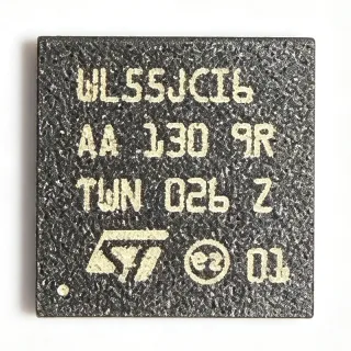
NRF51822-QFAC-R7 - Bluetooth LE/ANT SoC, 256KB Flash, QFN-48 | Nordic
部品番号: NRF51822-QFAC-R7 ✗ 生産終了| 数量 | 単価 | 小計 |
|---|---|---|
| 1 | $9.85 | $9.85 |
| 10 | $9.1 | $91.00 |
| 100 | $8.2 | $820.00 |
| 500 | $7.1 | $3,550.00 |
| 1,000 | $6.25 | $6,250.00 |
NRF51822-QFAC-R7 概要
A Bluetooth SoC (System-on-Chip) is a single integrated circuit that combines a microcontroller, radio transceiver, memory, and peripherals required to implement a complete wireless connectivity solution. The nRF51822 sits within the broader product taxonomy of wireless MCUs -> 2.4 GHz transceivers -> RF & Wireless ICs. By collapsing the radio and protocol stack into one die, SoCs reduce BOM count, PCB complexity, and total system power compared with discrete MCU-plus-transceiver designs.
Key features include a 32-bit ARM Cortex-M0 core running up to 16 MHz, a 2.4 GHz radio with -93 dBm RX sensitivity in BLE mode, integrated 16-channel AES encryption accelerator, 12-bit/200 ksps ADC, and a rich peripheral set (GPIO, SPI, I2C, UART, PWM, RTC). The device supports both Bluetooth low energy (v4.0/v4.2) and the ANT+ protocol, making it a versatile choice for wearables, sports sensors, beacons, and proprietary 2.4 GHz links.
Architecturally, the nRF51822 separates the application Cortex-M0 core from the radio front-end through a shared memory architecture. A built-in DC-DC converter improves power efficiency at higher supply voltages, while an LDO mode is available for low-Iq designs. The part also includes a wake-on-radio function for ultra-low standby current.
Typical applications include Bluetooth Low Energy beacons, fitness wearables, medical sensors, smart-home nodes, and industrial IoT endpoints. The QFAC variant with 256 KB flash is targeted at applications requiring OTA firmware updates or richer protocol stacks.
A critical design consideration is antenna matching: the QFN package's single-ended RFIO pin requires a π-network matching network between the chip and antenna (typically chip or trace antenna) to meet Bluetooth 5.2 sub-1 GHz emissions. Decoupling capacitors must be placed close to the supply pins, and the DC-DC inductor must be shielded. Routing the exposed pad to a flooded ground plane is required for thermal dissipation.
This page consolidates distributor pricing, drop-in alternatives, and practical design notes - including same-brand Nordic variants and cross-brand equivalents - offering engineering value not found in the standalone datasheet.
ドロップイン代替品: NRF51822-QFAC-R7 — 同一パッケージでピン互換。PCBの作り直しが必要な異なるパッケージの部品は除外されています。
クイック比較ツール — 並列比較する代替部品を選択:
NRF51822-QFAA-R
✅ ドロップイン📋 参考代替品(カタログ未掲載)
NRF51822-QFAC-R
✅ ドロップイン ⚠️ 仕様未検証📋 参考代替品(カタログ未掲載)
NRF52810-QFAA-R
✅ ドロップイン📋 参考代替品(カタログ未掲載)
NRF52832-QFAA-R
✅ ドロップイン📋 参考代替品(カタログ未掲載)
NRF51422-QFAC-R
✅ ドロップイン📋 参考代替品(カタログ未掲載)
NRF51802-QFAA-R
✅ ドロップイン📋 参考代替品(カタログ未掲載)
NRF51822-QFAC-R7 最大定格&電気的特性
| Core Architecture | ARM Cortex-M0, 32-bit |
| 最大クロック周波数 | 16 MHz |
| Flash Memory | 256 KB |
| RAM | 32 KB |
| Operating Voltage | 1.8 V to 3.6 V |
| Radio Frequency | 2.4 GHz (2400 MHz to 2483.5 MHz) |
| Supported Protocols | Bluetooth low energy v4.0/v4.2, ANT+, 2.4 GHz proprietary |
| TX Output Power | -20 dBm to +4 dBm |
| RX Sensitivity (BLE 1 Mbps) | -93 dBm |
| AES Encryption Accelerator | 16-channel hardware AES-ECB |
| ADC | 10-bit, 8 channels |
| 動作温度範囲 | -40 C to +85 C |
| パッケージ | 48-pin QFN with exposed pad (6x6 mm) |
| 実装タイプ | Surface Mount |
| MSLレベル | 3 (168 hours) |
| RoHS ステータス | Compliant |
| DC-DC Converter | Integrated (selectable LDO mode) |
NRF51822-QFAC-R7 48-pin qfn with exposed pad (6x6 mm) ピン配置ガイド
NRF51822-QFAC-R7 (48-pin qfn with exposed pad (6x6 mm) パッケージ) のピン配置。 このデジタルICには、GPIO、通信インターフェース (UART、SPI、I2C)、および電源ピンが含まれています。代替ピン機能と設定オプションについては、メーカーのデータシートを参照してください。組み込みシステム設計とPCBレイアウトに不可欠です。

詳細なピン配置データはありません: NRF51822-QFAC-R7.
詳細は データシート をご参照ください。
主な用途
NRF51822-QFAC-R7 の用途: 6 件s: Bluetooth Low Energy Beacons, Wearable Fitness and Health Sensors, Smart Home IoT Endpoints, Medical Wireless Sensor Patches, Industrial IoT Wireless Modules, Wireless HID and Remote Controls.
Bluetooth Low Energy Beacons
The NRF51822-QFAC-R7 is widely deployed in BLE beacons for retail proximity marketing, asset tracking, and indoor wayfinding. Its -93 dBm RX sensitivity and +4 dBm TX power enable line-of-sight ranges of 30-50 m using a trace antenna, while the 256 KB flash accommodates iBeacon, Eddystone, and proprietary beacon profiles side-by-side. The integrated DC-DC converter keeps average beacon current under 25 µA at 1 Hz advertising, allowing 2-3 years of operation from a single CR2032 coin cell when TX duty cycle is optimized.
おすすめ
Wearable Fitness and Health Sensors
Wristbands, heart-rate straps, and running watches benefit from the NRF51822-QFAC-R7's low power and small QFN-48 (6x6 mm) footprint. The Cortex-M0 core runs sensor-fusion algorithms at under 5 mA active, and the 256 KB flash stores ANT+ device profiles plus BLE GATT services for multi-protocol fitness hubs. With -40 °C to +85 °C operation and 1.8 V minimum supply, the part is qualified for skin-contact and cold-weather outdoor sports use.
おすすめ
Smart Home IoT Endpoints
Smart-home sensors - temperature, door/window, leak, occupancy - leverage the NRF51822-QFAC-R7's Cortex-M0 + 2.4 GHz radio combination for coin-cell-powered BLE mesh nodes. The chip's hardware AES-ECB accelerator secures proprietary or BLE-mesh payloads with negligible CPU overhead, while the integrated 12-bit ADC directly reads thermistor or PIR outputs without an external ADC. Production code typically fits in under 180 KB flash, leaving headroom for OTA updates.
おすすめ
Medical Wireless Sensor Patches
Single-use medical patches for continuous patient monitoring (temperature, hydration, wound status) use the NRF51822-QFAC-R7's small footprint, low power, and integrated security. The hardware AES accelerator secures HIPAA-relevant patient data in transit, and the 32 KB RAM buffers multi-sensor fusion outputs between BLE transmissions. BLE link-layer encryption via AES-CCM provides medical-grade confidentiality without external crypto ICs.
おすすめ
Industrial IoT Wireless Modules
Industrial predictive-maintenance sensors - vibration, current, temperature on motors - use the NRF51822-QFAC-R7 to transmit telemetry over BLE or 2.4 GHz proprietary links to gateways. The -40 °C to +85 °C operating range covers most factory-floor enclosures, and the Cortex-M0 can run FFT preprocessing on vibration data before transmission, reducing radio duty cycle by 5-10x. Nordic's Gazell protocol enables sub-2 ms latency star networks for time-critical industrial nodes.
おすすめ
Wireless HID and Remote Controls
Wireless keyboards, presentation clickers, and game controllers use the NRF51822-QFAC-R7's proprietary 2.4 GHz modes for sub-8 ms input latency. The hardware AES-ECB secures HID pairing, and the low standby current (under 1.5 µA in System OFF) suits AAA-battery-powered remotes with 5+ year battery life. The QFN-48 (6x6 mm) package plus four PFWs fit inside the tight mechanical envelope of compact clickers and presenter remotes.
おすすめ
おすすめ製品の概要
エンジニアリング参考データ: NRF51822-QFAC-R7 — 比較、設計ガイダンス、コンプライアンス情報。
選定ガイド
代替品との比較
| パラメータ | この製品 | NRF51822-QFAA-R | NRF52810-QFAA-R | NRF52832-QFAA-R | NRF51422-QFAC-R | NRF51802-QFAA-R |
|---|---|---|---|---|---|---|
| Brand | Nordic Semiconductor | Nordic Semiconductor | Nordic Semiconductor | Nordic Semiconductor | Nordic Semiconductor | Nordic Semiconductor |
| Package | QFN-48 (6x6 mm) | QFN-48 (6x6 mm) | QFN-48 (6x6 mm) | QFN-48 (6x6 mm) | QFN-48 (6x6 mm) | QFN-48 (6x6 mm) |
| Core | ARM Cortex-M0 @ 16 MHz | ARM Cortex-M0 @ 16 MHz | ARM Cortex-M4 @ 64 MHz | ARM Cortex-M4F @ 64 MHz | ARM Cortex-M0 @ 16 MHz | ARM Cortex-M0 @ 16 MHz |
| Flash / RAM | 256 KB / 32 KB | 128 KB / 16 KB | 192 KB / 24 KB | 512 KB / 64 KB | 256 KB / 32 KB | 256 KB / 32 KB |
| Bluetooth Version | BLE 4.0 / 4.2 | BLE 4.0 / 4.2 | Bluetooth 5 | Bluetooth 5 | ANT/ANT+ (BLE disabled) | BLE 4.0 / 4.2 |
| TX Power Range | -20 to +4 dBm | -20 to +4 dBm | -20 to +4 dBm | -20 to +4 dBm | -20 to +4 dBm | -20 to 0 dBm (no +4 dBm) |
| RX Sensitivity (BLE 1M) | -93 dBm | -93 dBm | -96 dBm | -96 dBm | -93 dBm | -91 dBm |
| Operating Voltage | 1.8 V to 3.6 V | 1.8 V to 3.6 V | 1.7 V to 3.6 V | 1.7 V to 3.6 V | 1.8 V to 3.6 V | 1.8 V to 3.6 V |
| Lifecycle Status | NRND | NRND | Active | Active | NRND | NRND |
| Approx Unit Price (qty 1000) | $6.25 | $5.65 | $5.20 | $8.40 | $6.40 | $4.90 |
主な差別化要因
- 256 KB flash with full BLE/ANT multiprotocol support (vs NRF51822-QFAA-R)
- Pin-compatible upgrade to Bluetooth 5 with Cortex-M4 (vs NRF52832-QFAA-R)
- ANT+ protocol enabled for sports/medical hubs (vs NRF51422-QFAC-R)
設計ノート
The NRF51822-QFAC-R7 requires a π-network matching network (typically 2.2 nL and 1.5 pF components) between the RFIO pin and the antenna to achieve -93 dBm RX sensitivity and meet FCC/CE emissions. The exposed thermal pad is the chip's main RF ground - flood all four layers beneath the QFN with continuous ground copper and stitch with 8-12 thermal vias (0.3 mm drill, 0.5 mm pitch). RF traces must be 50 Ω controlled-impedance (microstrip or coplanar waveguide), and decoupling capacitors (100 nF + 1 nF) must be placed within 1 mm of each VDD pin.
The integrated DC-DC converter mode reduces peak current draw by 30-40% compared to LDO mode at supply voltages above 2.0 V. Place the DC-DC inductor (10 µH, X5R, 0805) and its 100 nF bypass capacitor within 2 mm of the DEC1/DEC2 pins. For battery-critical coin-cell designs, switch to LDO mode below 2.0 V to eliminate DC-DC switching noise on the ADC and improve sleep current by 1-2 µA.
Do not load the SoftDevice into the upper 88 KB of flash on the -QFAC variant unless you have reserved flash for application code - typical SoftDevice S110 (BLE peripheral) is 96 KB and S120 (BLE central) is 96 KB. Choose SoftDevice size before committing to memory-mapped storage. Also, the GPIO drive strength is limited to 5 mA per pin; do not drive high-current LEDs directly without a MOSFET. The ADC reference voltage is internally tied to VDD - calibrate ADC readings against VDD to compensate for coin-cell discharge.
Estimated: at continuous +4 dBm TX, the NRF51822-QFAC-R7 draws up to 16 mA from a 3.6 V supply, dissipating ~57 mW in the die. With the QFN-48 package's theta_JA of approximately 40 °C/W (per Nordic's reference design), this yields a 2.3 °C junction rise above ambient - well within the +85 °C operating limit. However, in a sealed enclosure without airflow, add a 1-2 °C/W thermal margin when budgeting for sustained TX duty cycles above 50%.
コンプライアンス情報
RoHS compliant per Nordic product page. Not AEC-Q100 qualified; for automotive designs use nRF52832-AEC-Q100 variants. Bluetooth 4.0/4.2 qualified by Bluetooth SIG.