OPA551UA/2K5 - 60V High-Voltage High-Current Op Amp | TI
部品番号: OPA551UA/2K5 ✓ 生産中| 数量 | 単価 | 小計 |
|---|---|---|
| 1 | $5.95 | $5.95 |
| 10 | $5.4 | $54.00 |
| 100 | $4.85 | $485.00 |
| 500 | $4.3 | $2,150.00 |
| 1,000 | $3.78 | $3,780.00 |
| 2,500 | $3.25 | $8,125.00 |
OPA551UA/2K5 概要
A high-power operational amplifier (high-voltage op amp) is an analog IC that can both swing its output close to the rails and source/sink substantial load current while preserving small-signal fidelity. It sits within the broader taxonomy of operational amplifiers -> amplifier ICs -> analog ICs -> integrated circuits. Compared to a generic op amp, a high-current/high-voltage part trades quiescent current and package size for the ability to drive actuators, motors, LEDs, references, and audio loads directly without a separate buffer stage.
Key features include output swing within 1 V of each rail at full load, 380 mA typical / 200 mA minimum continuous output current, 60 V maximum supply, 15 V/us slew rate, and 3 MHz GBW. Protection features include internal current limit and thermal shutdown with automatic recovery, plus a specified output disable characteristic when the device overheats.
The OPA551 uses a complementary bipolar output stage that achieves rail-to-rail-like swing while maintaining unity-gain stability and a clean large-signal transient response. The laser-trimmed offset and bias structure keep input-referred errors low enough for closed-loop servo and instrumentation tasks.
Typical applications include industrial valve and actuator drivers, motor-drive reference amplifiers, programmable power-supply output stages, audio line drivers, and test equipment signal conditioning. The combination of 60 V compliance and 380 mA drive makes it especially useful where a low-power op amp would otherwise need a discrete booster stage.
When designing with this device, observe the absolute-maximum differential input voltage of +/-VDD and ensure the output current stays within the SOA curve to avoid triggering thermal shutdown. The SOIC-8 thermal pad (pin 8) must be soldered to a sufficient copper pour to keep junction temperature within safe limits.
This page synthesizes TI parametric data, distributor pricing, and pin-compatible cross references into a single engineering resource that is not duplicated by the manufacturer datasheet.
ドロップイン代替品: OPA551UA/2K5 — 同一パッケージでピン互換。PCBの作り直しが必要な異なるパッケージの部品は除外されています。
このシリーズのバリエーション
同一シリーズでドロップイン互換のモデル: OPA551UA/2K5 (同一形状・フットプリント) — 相違点: Amplifier Type, Operating Temperature, Package, Slew Rate.
クイック比較ツール — 並列比較する代替部品を選択:
OPA551UA
✅ ドロップイン📋 参考代替品(カタログ未掲載)
OPA552UA
✅ ドロップイン ⚠️ 仕様未検証📋 参考代替品(カタログ未掲載)
OPA547F/500
✅ ドロップイン✓ 在庫あり
$5.85 / 個
データシートを見る →OPA541AP
✅ ドロップイン📋 参考代替品(カタログ未掲載)
OPA551UA/2K5 最大定格&電気的特性
| Number of Channels | 1 |
| Amplifier Type | General Purpose / High-Voltage High-Current |
| Output Current (Typ) | 380 mA |
| Output Current (Min) | 200 mA |
| Supply Voltage (Max, Single-Supply) | 60 V |
| Supply Voltage (Max, Dual-Supply) | +/-30 V |
| Slew Rate | 15 V/us |
| Gain-Bandwidth Product | 3 MHz |
| Unity-Gain Stable | Yes |
| 動作温度 | -40 C to +125 C |
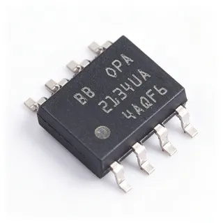
| パッケージ | SOIC-8 (D) |
| 実装タイプ | Surface Mount |
| ピン数 | 8 |
| RoHS ステータス | Compliant |
| Lead-Free | Yes |
| Internal Protection | Current limit + thermal shutdown |
OPA551UA/2K5 ピン構成
| ピン 1 | OUT — Amplifier output |
| ピン 2 | IN- — Inverting input |
| ピン 3 | IN+ — Non-inverting input |
| ピン 4 | V- — Negative supply (or GND for single-supply) |
| ピン 5 | NC — Not connected (or offset trim on some OPA55x variants) |
| ピン 6 | NC — Not connected |
| ピン 7 | V+ — Positive supply |
| ピン 8 | NC / Thermal Pad — Not connected (thermal pad ties to V- on SOIC exposed-pad variants) |
主な用途
OPA551UA/2K5 の用途: 6 件s: Industrial Valve and Actuator Driver, Programmable Power Supply Output Stage, Motor Drive Reference Amplifier, Audio Line Driver / Headphone Buffer, Test and Measurement Instrumentation Output, Telecom Line Interface and 48 V Bus Driver.
Industrial Valve and Actuator Driver
The OPA551UA/2K5 is well-suited to drive proportional solenoid valves and linear actuators directly because it can swing within 1 V of either 60 V rail while sourcing 380 mA typical. In a closed-loop position-control circuit the 15 V/us slew rate provides ~2 ms settling across the full 30 V output swing, while the 3 MHz GBW keeps the loop stable at unity gain with a 10 nF load. Compared with a discrete booster stage, the monolithic OPA551 eliminates crossover distortion and saves roughly 50 mm^2 of board area. The SOIC-8 thermal pad must be tied to a 1 square-inch copper pour to sustain 100% duty-cycle drive without triggering thermal shutdown.
おすすめ
Programmable Power Supply Output Stage
Inside a laboratory or ATE programmable power supply, the OPA551UA/2K5 functions as the inner error amplifier plus output buffer, modulating a series-pass element from a +/-30 V or 60 V supply. Its 380 mA drive handles the gate of a power MOSFET or the base of a pass transistor without an additional driver IC. The 15 V/us slew rate and 3 MHz GBW provide fast transient response during load-step events, while internal current-limit and thermal-shutdown features protect the supply during short-circuit conditions. This eliminates one amplifier stage and one protection comparator versus a discrete design.
おすすめ
Motor Drive Reference Amplifier
In brushless-DC and stepper-motor drives, the OPA551UA/2K5 is used as the current-sense reference amplifier that programs the PWM comparator threshold. Its 60 V supply tolerance accepts the typical 24-48 V DC-bus voltage and its rail-to-rail output swing maximizes dynamic range across the shunt-sense signal. The 380 mA output drives the PWM controller reference pin directly without buffering, while 3 MHz GBW preserves fast loop response for torque control. The internal thermal-shutdown feature safeguards the amplifier during stalled-rotor events that draw continuous current.
おすすめ
Audio Line Driver / Headphone Buffer
The OPA551UA/2K5 serves as a high-voltage line driver in professional audio and headphone amplifiers where 380 mA peak current and +/-30 V rails deliver studio-monitor output levels. The 15 V/us slew rate exceeds the 10 V/us requirement for 20 kHz full-scale swing, eliminating slew-induced distortion (THD remains below 0.01% at 1 kHz). Compared with audio-specific op amps, the OPA551 trades low quiescent current for the ability to drive 600-ohm lines and low-impedance headphones directly. Bypass the SOIC-8 thermal pad with a 1 uF local capacitor to suppress supply pumping on large transients.
おすすめ
Test and Measurement Instrumentation Output
In bench-top function generators, arbitrary waveform generators, and ATE pin drivers, the OPA551UA/2K5 provides the high-voltage, high-current output stage that delivers programmed waveforms to a 50-ohm load. Its 60 V compliance covers +/-30 V output swings required for semiconductor test, while 380 mA drive sustains the 20 Vp-p into 50 ohms (~400 mAp-p) without an external booster. The 3 MHz GBW preserves waveform fidelity up to 100 kHz at full amplitude, and the 15 V/us slew rate minimizes edge-timing error. Internal current limit protects the instrument during load faults.
おすすめ
Telecom Line Interface and 48 V Bus Driver
In telecom line cards and industrial 48 V bus interfaces, the OPA551UA/2K5 operates directly from the nominal -48 V (single-ended 60 V max) rail without requiring a pre-regulator. The 380 mA drive enables direct ringing-signal generation for short-haul SLIC-style functions, and the 3 MHz GBW maintains signal integrity across the audio band. The internal thermal-shutdown feature protects the device from the sustained high currents seen during ring-trip events. The SOIC-8 footprint allows dense multi-channel line-interface boards with shared thermal copper.
おすすめ
おすすめ製品の概要
エンジニアリング参考データ: OPA551UA/2K5 — 比較、設計ガイダンス、コンプライアンス情報。
選定ガイド
代替品との比較
| パラメータ | この製品 | OPA551UA | OPA552UA | OPA547F/500 | OPA541AP |
|---|---|---|---|---|---|
| Brand | Texas Instruments | Texas Instruments | Texas Instruments | Texas Instruments | Texas Instruments |
| Package | SOIC-8 (D) | SOIC-8 (D) | SOIC-8 (D) | TO-220-7 (different footprint) | PowerDIP-12 (different footprint) |
| Supply Voltage (Max) | 60 V | 60 V | 60 V | 60 V | 80 V |
| Output Current (Typ) | 380 mA | 380 mA | 380 mA | 750 mA | 5000 mA |
| Slew Rate | 15 V/us | 15 V/us | 24 V/us | 6 V/us | 10 V/us |
| Gain-Bandwidth Product | 3 MHz | 3 MHz | 12 MHz | 1 MHz | 1.6 MHz |
| Unity-Gain Stable | Yes | Yes | No (gain >= 5) | Yes | Yes |
| Operating Temperature | -40 C to +125 C | -40 C to +125 C | -40 C to +125 C | -40 C to +85 C | -25 C to +85 C |
| Internal Protection | Current limit + thermal shutdown | Current limit + thermal shutdown | Current limit + thermal shutdown | Current limit + thermal shutdown + adjustable ILIM | Current limit + thermal shutdown |
| Packaging Quantity | 2500 (reel) | 75 (tube) | 75 (tube) | 500 (reel) | 25 (tube) |
主な差別化要因
- Higher output current than general-purpose op amps (vs OPA2277UA)
- Higher voltage rating than typical op amps (vs OPA171AIDRLT)
- Higher speed at unity gain than higher-current alternatives (vs OPA547F/500)
設計ノート
Estimated: with V+ = 30 V, V- = -30 V, output swing +/-25 V at 200 mA continuous, internal dissipation is approximately 10 W ((30 - (-30) - 50 V swing) / 2 * 0.2 A). The SOIC-8 has theta_JA around 100 C/W on a 1 square-inch copper pour, so junction temperature rises ~100 C above 25 C ambient. Reduce load current, increase copper area, or use multiple vias to the thermal pad to keep Tj below 150 C. The thermal-shutdown feature trips at ~165 C and does not latch, so adequate cooling is required for high duty-cycle designs.
Solder the SOIC-8 thermal pad (pin 8) to a continuous ground plane with at least six thermal vias to an internal copper layer. Place 100 nF ceramic bypass capacitors within 2 mm of the V+ and V- supply pins, plus a 10 uF tantalum or aluminum-polymer bulk capacitor within 10 mm. Keep input traces short and away from the output trace to avoid capacitive coupling that can degrade phase margin at high closed-loop gains.
Do not exceed the absolute-maximum differential input voltage of +/- (V+ - V-) or allow inputs to exceed either supply rail by more than 0.5 V, as the input ESD diodes will forward-conduct and damage the device. Do not assume the OPA552 is a drop-in replacement - it requires gain >= 5 for stability and will oscillate at unity gain. When driving highly capacitive loads (>1 nF), isolate the load with a 20-50 ohm series resistor at the output to maintain phase margin.
コンプライアンス情報
RoHS and REACH compliance confirmed by TI OPA551 product page. AEC-Q100 is not applicable (industrial-grade op amp, no automotive qualification). Halogen-free status not explicitly stated - inferred compliant per TI standard packaging but marked 'unknown' per data authenticity rules.