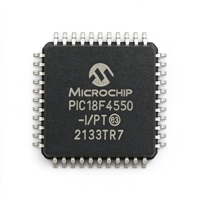
PIC18F4550-I/PT - 8-bit 32KB Flash USB MCU | Microchip
部品番号: PIC18F4550-I/PT ✓ 生産中| 数量 | 単価 | 小計 |
|---|---|---|
| 1 | $8.36 | $8.36 |
| 10 | $7.52 | $75.20 |
| 100 | $6.78 | $678.00 |
| 500 | $6.1 | $3,050.00 |
| 1,000 | $5.5 | $5,500.00 |
| 3,000 | $4.95 | $14,850.00 |
PIC18F4550-I/PT 概要
A PIC18F-series 8-bit microcontroller is part of the PIC microcontroller family from Microchip Technology - an 8-bit Harvard-architecture RISC MCU built around a small instruction set that allows single-cycle execution and predictable interrupt latency. The PIC18 line extends the PIC16 base with linear memory addressing, larger RAM/Flash, hardware multiplier, and C-friendly architecture, sitting between legacy PIC16 parts and the 16-bit dsPIC/PIC24 families. PIC18F parts with integrated USB are particularly common in low-cost embedded USB device designs where an external PHY is undesirable.
Key features of the PIC18F4550 include: 32 KB self-programmable Flash, 2 KB SRAM, 256 B EEPROM, 13 channels of 10-bit ADC, two 8-bit timers plus three 16-bit timers, two capture/compare/PWM modules, an enhanced USART with LIN support, an MSSP module that can operate in I2C or SPI mode, an on-chip Full-Speed USB 2.0 device/host/OTG transceiver, and nanoWatt sleep/idle modes that drop current consumption into the microampere range.
The device uses a 16-bit instruction word with an 8-bit data path, a hardware multiply (8x8 in one cycle), an 8-level hardware stack, and a priority-vectored interrupt controller. The integrated USB SIE handles endpoint management without CPU intervention, leaving the application CPU free to handle class-level stacks such as HID, CDC, or vendor-class. Code protection and an ICD/ICSP debug interface are standard on the silicon.
Typical applications include USB HID peripherals (keyboards, mice, custom input devices), CDC virtual COM port bridges, USB-to-UART converter dongles, low-cost data loggers, educational microcontroller boards, and industrial sensor interfaces where LIN/EUSART connectivity is required. The industrial -40C to +85C temperature grade also suits outdoor or factory-floor deployments.
When designing with the PIC18F4550-I/PT, ensure the USB bus pins (D+/D-) have a 90 ohm differential impedance to the connector, place the 470 nF VUSB bypass capacitor within 5 mm of the VUSB pin, and tie the VBUS sense pin to the 5 V from the host when bus-powered. The 48 MHz system clock requires a 20 MHz crystal on OSC1/OSC2 with the PLL configured in software; USB Full-Speed compliance requires this exact 48 MHz clock.
This page synthesizes distributor pricing, drop-in alternatives sourced from Microchip's own migration guides, and practical design notes not found in the manufacturer datasheet alone.
ドロップイン代替品: PIC18F4550-I/PT — 同一パッケージでピン互換。PCBの作り直しが必要な異なるパッケージの部品は除外されています。
このシリーズのバリエーション
同一シリーズでドロップイン互換のモデル: PIC18F4550-I/PT (同一形状・フットプリント) — 相違点: Timers, Package, ADC, Operating Temperature, Core Architecture.
クイック比較ツール — 並列比較する代替部品を選択:
PIC18F45K50-I/PT
✓ 在庫あり
$2.74 / 個
データシートを見る →PIC18F4455-I/PT
✓ 在庫あり
$4.85 / 個
データシートを見る →PIC18F4458-I/PT
✓ 在庫あり
$5.79 / 個
データシートを見る →PIC18F4550-I/P
📋 参考代替品(カタログ未掲載)
PIC18F4550-I/ML
📋 参考代替品(カタログ未掲載)
PIC18F4553-I/PT
📋 参考代替品(カタログ未掲載)
PIC18F4558-I/PT
📋 参考代替品(カタログ未掲載)
PIC18F4550-I/PT 最大定格&電気的特性
| Device Family | PIC18F |
| Core | 8-bit PIC RISC (Harvard) |
| Program Memory (Flash) | 32 KB (16K x 16) |
| Data SRAM | 2048 bytes |
| Data EEPROM | 256 bytes |
| Maximum CPU Frequency | 48 MHz (12 MIPS) |
| Supply Voltage (VDD) | 4.2 V to 5.5 V |
| I/O Pins | 35 |
| ADC | 10-bit, 13 channels |
| Timers | 1x 8-bit + 3x 16-bit |
| CCP/ECCP Modules | 2 |
| Serial Interfaces | USB 2.0 FS, EUSART (LIN), MSSP (I2C/SPI) |
| USB | Full-Speed 12 Mbit/s, integrated transceiver |
| パッケージ | TQFP-44 (10x10 mm, PT) |
| 実装タイプ | Surface Mount |
| 動作温度 | -40C to +85C (industrial, 'I') |
| MSLレベル | 3 (168 hours) |
| RoHS ステータス | Compliant |
PIC18F4550-I/PT ピン構成
| ピン 1 | MCLR/VPP/RE3 — Master Clear (reset) input / programming voltage / digital I/O RE3 |
| ピン 2 | RA0/AN0 — Digital I/O RA0 / analog input AN0 |
| ピン 3 | RA1/AN1 — Digital I/O RA1 / analog input AN1 |
| ピン 4 | RA2/AN2/VREF- — Digital I/O RA2 / AN2 / ADC VREF- |
| ピン 5 | RA3/AN3/VREF+ — Digital I/O RA3 / AN3 / ADC VREF+ |
| ピン 6 | RA4/T0CKI/C1OUT — Digital I/O RA4 / Timer0 clock / comparator 1 output |
| ピン 7 | RA5/AN4/SS/C2OUT — Digital I/O RA5 / AN4 / SPI SS / comparator 2 output |
| ピン 8 | RE0/RD — Digital I/O RE0 / parallel-port read strobe (PSP) |
| ピン 9 | RE1/WR — Digital I/O RE1 / parallel-port write strobe (PSP) |
| ピン 10 | RE2/CS — Digital I/O RE2 / parallel-port chip select (PSP) |
| ピン 11 | VDD — Positive supply (4.2-5.5 V) |
| ピン 12 | VSS — Ground reference |
| ピン 13 | OSC1/CLKI/RA7 — Crystal oscillator input / external clock / digital I/O RA7 |
| ピン 14 | OSC2/CLKO/RA6 — Crystal oscillator output / clock output / digital I/O RA6 |
| ピン 15 | RC0/T1OSO/T13CKI — Digital I/O RC0 / Timer1 oscillator out / Timer1/Timer3 clock |
| ピン 16 | RC1/T1OSI/CCP2 — Digital I/O RC1 / Timer1 oscillator in / CCP2 PWM output |
| ピン 17 | RC2/CCP1 — Digital I/O RC2 / CCP1 PWM output |
| ピン 18 | RC4/D-/VM — Digital I/O RC4 / USB D- / external USB transceiver VM |
| ピン 19 | RC5/D+/VP — Digital I/O RC5 / USB D+ / external USB transceiver VP |
| ピン 20 | RC6/TX/CK — Digital I/O RC6 / EUSART TX / EUSART synchronous clock |
| ピン 21 | RC7/RX/DT — Digital I/O RC7 / EUSART RX / EUSART synchronous data |
| ピン 22 | VUSB — Internal USB transceiver 3.3 V regulator output (470 nF bypass to ground) |
| ピン 23 | RD0/SCK/SDA — Digital I/O RD0 / MSSP SPI clock / MSSP I2C data |
| ピン 24 | RD1/SDI/SDA — Digital I/O RD1 / MSSP SPI data in / MSSP I2C data |
| ピン 25 | RD2/SDO — Digital I/O RD2 / MSSP SPI data out |
| ピン 26 | RD3/SS — Digital I/O RD3 / MSSP SPI slave select |
| ピン 27 | RB0/AN12/INT0 — Digital I/O RB0 / analog input AN12 / external interrupt 0 |
| ピン 28 | RB1/AN10/INT1 — Digital I/O RB1 / analog input AN10 / external interrupt 1 |
| ピン 29 | RB2/AN8/INT2 — Digital I/O RB2 / analog input AN8 / external interrupt 2 |
| ピン 30 | RB3/AN9/CCP2 — Digital I/O RB3 / analog input AN9 / CCP2 PWM output |
| ピン 31 | RB4/AN11 — Digital I/O RB4 / analog input AN11 |
| ピン 32 | RB5/AN13 — Digital I/O RB5 / analog input AN13 |
| ピン 33 | RB6/PGD — Digital I/O RB6 / ICSP data |
| ピン 34 | RB7/PGC — Digital I/O RB7 / ICSP clock |
| ピン 35 | VSS — Ground reference |
| ピン 36 | VDD — Positive supply (4.2-5.5 V) |
| ピン 37 | RD4 — Digital I/O RD4 |
| ピン 38 | RD5 — Digital I/O RD5 |
| ピン 39 | RD6 — Digital I/O RD6 |
| ピン 40 | RD7 — Digital I/O RD7 |
| ピン 41 | RC3 — Digital I/O RC3 |
| ピン 42 | RA5 — (see pin 7 - duplicate function note: digital I/O RA5) |
| ピン 43 | ICSPDAT — Dedicated ICSP data pin (TQFP-44 only) |
| ピン 44 | ICSPCLK — Dedicated ICSP clock pin (TQFP-44 only) |
主な用途
PIC18F4550-I/PT の用途: 7 件s: USB HID Peripheral Device, USB CDC Virtual COM Port Bridge, Industrial Sensor Interface with LIN Bus, Educational Microcontroller Trainer Board, USB Data Logger with On-Chip ADC, USB Custom Vendor-Class Device (LED Control, Test Equipment), USB-Enabled Home Automation / IoT Edge Node.
USB HID Peripheral Device
The PIC18F4550-I/PT is widely used to build USB HID-class peripherals such as custom keyboards, mice, game controllers, and industrial input panels. Its integrated Full-Speed USB 2.0 transceiver eliminates the need for an external PHY, while 32 KB of Flash comfortably holds HID descriptors plus application logic. The 35 GPIO pins provide enough I/O for matrix-scanned keypads and LED indicators, and the 10-bit ADC handles analog inputs like potentiometers or sliders. For HID polling under 1 ms intervals, the 48 MHz CPU clock leaves enough headroom for low-latency USB interrupt service routines.
おすすめ
USB CDC Virtual COM Port Bridge
A common application for the PIC18F4550-I/PT is building a USB-to-UART bridge that emulates a virtual COM port on the host side while exposing a true EUSART on the device side. The chip's MSSP and EUSART modules run independently from the USB stack, allowing concurrent asynchronous serial traffic and USB enumeration. The 2 KB SRAM holds USB CDC line-coding buffers and 16-byte transmit/receive FIFOs without DMA pressure. Industrial sensor and instrumentation manufacturers favor this topology because it avoids driver installation on modern Windows, Linux, and macOS hosts where CDC-ACM is in-box.
おすすめ
Industrial Sensor Interface with LIN Bus
The PIC18F4550-I/PT is well suited to industrial sensor nodes that need both USB diagnostics and LIN-bus field communication. The EUSART implements LIN 1.3 framing with hardware break detection and autobaud, while the integrated USB port lets the same node enumerate as a CDC device for factory-floor configuration and firmware update. The 13-channel 10-bit ADC reads up to 13 analog sensors directly, and the 256-byte EEPROM stores calibration constants. Industrial temperature grade (-40C to +85C) and 5 V tolerant I/O make the part a drop-in for 12 V/24 V industrial systems with a local 5 V rail.
おすすめ
Educational Microcontroller Trainer Board
The PIC18F4550-I/PT has long been a favorite on university microcontroller training boards because it combines a 5 V supply (which is forgiving for student labs), an integrated USB programmer/ICD interface, and enough peripherals (USB, ADC, PWM, I2C, SPI, EUSART) to teach an entire embedded curriculum in a single part. The 32 KB Flash comfortably fits a USB stack plus bootloader, leaving headroom for student C code. The TQFP-44 package is breadboardable with breakout adapters, and the ICSP pins allow in-circuit debug without removing the device.
おすすめ
USB Data Logger with On-Chip ADC
Low-cost, low-rate data loggers use the PIC18F4550-I/PT to sample analog signals at up to several kS/s and stream them over USB to a host PC for real-time display. The 13 ADC channels allow multi-sensor capture, while 2 KB of SRAM can buffer bursts between USB transfers. The 256-byte EEPROM retains log metadata (start time, calibration constants) across power cycles. With USB bus powering, the entire logger needs no external supply; the integrated USB transceiver handles all bus signalling. Firmware uses CDC for text streaming or vendor-class for higher throughput.
おすすめ
USB Custom Vendor-Class Device (LED Control, Test Equipment)
Many small-batch products - USB-controlled LED drivers, bench-test fixtures, and laboratory instruments - use the PIC18F4550-I/PT in vendor-class USB mode. The full-speed 12 Mbit/s bus and 48 MHz CPU support bulk transfers at near-megabyte-per-second rates, and 32 KB Flash leaves room for vendor-class descriptors plus application logic. The PWM modules drive LED current, the ADC reads test measurements, and the ICSP pins allow field firmware updates. Microchip's free USB stack (Microchip USB Framework) provides a turnkey vendor-class template for these designs.
おすすめ
USB-Enabled Home Automation / IoT Edge Node
Although the PIC18F4550-I/PT lacks built-in Wi-Fi, it serves well as an IoT edge node that pairs with an external ESP32 or Wi-Fi module over UART for tethered connectivity. USB is used for commissioning, firmware update, and local diagnostics, while the EUSART or MSSP handles the wireless module. The 32 KB Flash and 2 KB SRAM can run a small MQTT-over-TCP bridge or a custom IoT protocol. Industrial-grade temperature range and 5 V tolerance simplify integration with home-automation power rails and HVAC controls.
おすすめ
おすすめ製品の概要
エンジニアリング参考データ: PIC18F4550-I/PT — 比較、設計ガイダンス、コンプライアンス情報。
選定ガイド
代替品との比較
| パラメータ | この製品 | PIC18F4550-I/P | PIC18F4550-I/ML | PIC18F4553-I/PT | PIC18F4558-I/PT | PIC18F45K50-I/PT |
|---|---|---|---|---|---|---|
| Package | TQFP-44 (PT, 10x10 mm) | DIP-40 - through-hole | QFN-44 - lower profile | TQFP-44 (PT) - same | TQFP-44 (PT) - same | TQFP-44 (PT) - same |
| Brand | Microchip Technology | Microchip Technology | Microchip Technology | Microchip Technology | Microchip Technology | Microchip Technology |
| Program Memory (Flash) | 32 KB | 32 KB | 32 KB | 32 KB | 32 KB | 32 KB |
| Data SRAM | 2048 bytes | 2048 bytes | 2048 bytes | 2048 bytes | 2048 bytes | 2048 bytes |
| Maximum CPU Frequency | 48 MHz / 12 MIPS | 48 MHz / 12 MIPS | 48 MHz / 12 MIPS | 48 MHz / 12 MIPS | 48 MHz / 12 MIPS | 48 MHz / 12 MIPS |
| Supply Voltage (VDD) | 4.2 V to 5.5 V | 4.2 V to 5.5 V | 4.2 V to 5.5 V | 4.2 V to 5.5 V | 4.2 V to 5.5 V | 1.8 V to 5.5 V (wider) |
| USB 2.0 Transceiver | Yes (integrated) | Yes | Yes | Yes | Yes | Yes |
| Extra Peripheral vs F4550 | - | Same die | Same die | + CTMU touch-sensing | + Enhanced analog comparator | + Internal 48 MHz oscillator |
| Pin Count | 44 (TQFP) | 40 (DIP) | 44 (QFN) | 44 (TQFP) | 44 (TQFP) | 44 (TQFP) |
主な差別化要因
- Integrated Full-Speed USB 2.0 transceiver with on-chip SIE (vs PIC18F4520-I/P)
- More Flash memory (32 KB vs 16 KB) than PIC18F452-I/P (vs PIC18F452-I/P)
- Direct drop-in compatibility with PIC18F45K50-I/PT for low-voltage designs (vs PIC18F45K50-I/PT)
- Three independent serial ports vs two on PIC18F4520 (vs PIC18F4520-I/PT)
設計ノート
Estimated: Place the 470 nF VUSB bypass capacitor within 5 mm of the VUSB pin (TQFP-44 pin 22) to ensure USB Full-Speed compliance. Route the USB D+ (RC5, pin 19) and D- (RC4, pin 18) as a 90 ohm differential pair to the USB connector; match lengths to within 150 mil. Keep digital switching traces (PWM, SPI) away from the analog AVdd/AVss pins and route ADC inputs with ground guarding for best ADC accuracy.
The PIC18F4550-I/PT requires 4.2 V to 5.5 V on VDD per the datasheet. USB-powered designs must place a 10 uF bulk capacitor and a 0.1 uF decoupling capacitor on each VDD pin. The internal USB 3.3 V regulator on the VUSB pin supplies the on-chip transceiver and must NOT be loaded externally. For bus-powered designs, monitor the VBUS sense line in firmware to handle USB suspend/resume state correctly.
USB Full-Speed operation requires exactly 48 MHz CPU clock - do not use the internal 8 MHz oscillator without enabling the PLL and configuring the OSCTUNE register properly. Forget the configuration-bit _CPUDIV_OSC1_PLL2_3L_ and the _FOSC_HSPLL_HS_ setting, and the USB stack will enumerate at the wrong speed and fail USB compliance. Also ensure that the USB internal transceiver mode (configuration bit _UTSEL_Internal_Transceiver_) is set rather than the external-transceiver mode for the F4550 family.
Estimated: At maximum CPU load (48 MHz, all peripherals active), the TQFP-44 package dissipates approximately 100 mW with theta_JA near 50 C/W on a standard 4-layer JEDEC test board, giving a 5 C junction rise above ambient. This is well within the industrial -40C to +85C operating range and typically requires no heatsinking. For sealed enclosures with no airflow, derate the operating ambient by 5-10 C if sustained USB traffic drives sustained internal current.
コンプライアンス情報
RoHS and REACH compliant per Microchip product page. Industrial temperature grade -40C to +85C; not AEC-Q100 automotive qualified. The PIC18F4550-I/PT and -I/ML variants are Pb-free; the older PIC18F4550-I/P may have different compliance status - check lot markings.







