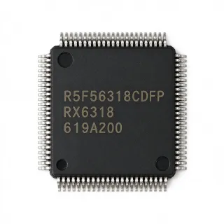
R5F52316ADFP#10 - 54MHz RX231 256KB Flash MCU | Renesas
部品番号: R5F52316ADFP#10 ✓ 生産中| 数量 | 単価 | 小計 |
|---|---|---|
| 1 | $9.5 | $9.50 |
| 10 | $8.55 | $85.50 |
| 100 | $7.6 | $760.00 |
| 500 | $6.85 | $3,425.00 |
| 1,000 | $6.1 | $6,100.00 |
R5F52316ADFP#10 概要
What is a low-power high-performance RX MCU? The RX231 belongs to Renesas' RX200 family of low-power 32-bit microcontrollers based on the RXv2 architecture, which combines an enhanced Harvard bus with a hardware FPU and DSP extensions. Within the broader taxonomy, R5F52316ADFP#10 is a microcontroller (MCU) -> embedded processor -> semiconductor, positioned for energy-conscious applications that still require DSP-class math and rich connectivity.
Key features include a wide operating voltage range from 1.8 V to 5.5 V, integrated 12-bit A/D converter with up to 4 channels of D/A, real-time clock, and security functions such as a unique hardware ID and AES-style acceleration. It also integrates a capacitive touch sensing unit (CTSU) that simplifies implementing waterproof touch buttons and sliders without external components. Multiple low-power modes - including deep software standby drawing only a few microamps - extend battery life across portable and always-on use cases.
From an architectural standpoint, the RXv2 core features a 5-stage pipeline, single-cycle MAC, and dedicated FPU, achieving up to 1.65 DMIPS/MHz. The MCU supports up to 70 GPIO pins, multiple serial interfaces (SCI, I2C, SPI, RSPI), and an external bus interface for memory expansion. ECC on flash and SRAM, watchdog timers, and a low-voltage detector add functional-safety features that simplify IEC/UL consumer-safety designs.
Typical applications include home appliances with touch UI, IoT sensor nodes, USB peripherals, industrial HMI panels, and low-power connected medical devices. The wide 5.5 V tolerance also makes the device robust in 24 V industrial bus systems after simple LDO regulation.
When designing with R5F52316ADFP#10, evaluate the 5 V-tolerant GPIO count and the integrated CTSU to reduce BOM in touch-UI designs. For production programming, Renesas' e2 studio and the Flash Development Toolkit support on-board programming via the SCI bootloader.
This page synthesizes distributor pricing, cross-brand pin-compatible alternatives, and design notes not duplicated on the manufacturer product page.
ドロップイン代替品: R5F52316ADFP#10 — 同一パッケージでピン互換。PCBの作り直しが必要な異なるパッケージの部品は除外されています。
このシリーズのバリエーション
同一シリーズでドロップイン互換のモデル: R5F52316ADFP#10 (同一形状・フットプリント) — 相違点: Core Architecture, DSP Extensions, FPU, Maximum CPU Clock, Operating Temperature.
クイック比較ツール — 並列比較する代替部品を選択:
R5F52318ADFP
✅ ドロップイン📋 参考代替品(カタログ未掲載)
R5F52316CDFP#10
✅ ドロップイン📋 参考代替品(カタログ未掲載)
R5F52316ADFP#30
✅ ドロップイン📋 参考代替品(カタログ未掲載)
R5F52313ADFP
✅ ドロップイン📋 参考代替品(カタログ未掲載)
R5F52315ADFP
✅ ドロップイン ⚠️ 仕様未検証📋 参考代替品(カタログ未掲載)
R5F52316ADFP#10 最大定格&電気的特性
| Core Architecture | RXv2 (32-bit) |
| CPU Core | RX231 |
| FPU | Yes (single-precision) |
| DSP Extensions | Yes (enhanced DSP) |
| Maximum Operating Frequency | 54 MHz |
| Performance | 88.56 DMIPS |
| Program Memory (Flash) | 256 KB |
| RAM | 32 KB |
| Operating Voltage Range | 1.8 V to 5.5 V |
| 動作温度範囲 | -40 C to +85 C |
| パッケージ | 100-LFQFP (14x14 mm) |
| 実装タイプ | Surface Mount |
| GPIO Count | up to 70 |
| USB | USB 2.0 Full-Speed Host/Function/OTG |
| CAN | Yes (1 channel) |
| Capacitive Touch Sensing Unit (CTSU) | Yes (integrated) |
| A/D Converter | 12-bit |
| RoHS ステータス | Compliant |
R5F52316ADFP#10 ピン構成
| ピン 1 | VCC — Power supply (1.8 V to 5.5 V) |
| ピン 2 | PA0/IRQ0 — GPIO port A bit 0 / external interrupt 0 |
| ピン 3 | PA1/IRQ1 — GPIO port A bit 1 / external interrupt 1 |
| ピン 4 | PA2/IRQ2 — GPIO port A bit 2 / external interrupt 2 |
| ピン 5 | PA3/IRQ3 — GPIO port A bit 3 / external interrupt 3 |
| ピン 6 | PA4/IRQ4 — GPIO port A bit 4 / external interrupt 4 |
| ピン 7 | PA5/IRQ5 — GPIO port A bit 5 / external interrupt 5 |
| ピン 8 | PA6/IRQ6 — GPIO port A bit 6 / external interrupt 6 |
| ピン 9 | PA7/IRQ7 — GPIO port A bit 7 / external interrupt 7 |
| ピン 10 | VSS — Ground |
| ピン 11 | PB0 — GPIO port B bit 0 |
| ピン 12 | PB1 — GPIO port B bit 1 |
| ピン 13 | PB2 — GPIO port B bit 2 |
| ピン 14 | PB3 — GPIO port B bit 3 |
| ピン 15 | PB4 — GPIO port B bit 4 |
| ピン 16 | PB5 — GPIO port B bit 5 |
| ピン 17 | PB6 — GPIO port B bit 6 |
| ピン 18 | PB7 — GPIO port B bit 7 |
| ピン 19 | PC0 — GPIO port C bit 0 |
| ピン 20 | PC1 — GPIO port C bit 1 |
| ピン 21 | PC2 — GPIO port C bit 2 |
| ピン 22 | PC3 — GPIO port C bit 3 |
| ピン 23 | PC4 — GPIO port C bit 4 |
| ピン 24 | PC5 — GPIO port C bit 5 |
| ピン 25 | PC6 — GPIO port C bit 6 |
| ピン 26 | PC7 — GPIO port C bit 7 |
| ピン 27 | VCL — Decoupling capacitor pin |
| ピン 28 | RESn — Reset input, active low |
| ピン 29 | XTAL — System clock crystal |
| ピン 30 | EXTAL — System clock external clock input |
| ピン 31 | MD — Mode select pin (boot mode) |
| ピン 32 | PE0 — GPIO port E bit 0 |
| ピン 33 | PE1 — GPIO port E bit 1 |
| ピン 34 | PE2 — GPIO port E bit 2 |
| ピン 35 | PE3 — GPIO port E bit 3 |
| ピン 36 | PE4 — GPIO port E bit 4 |
| ピン 37 | PE5 — GPIO port E bit 5 |
| ピン 38 | PE6 — GPIO port E bit 6 |
| ピン 39 | PE7 — GPIO port E bit 7 |
| ピン 40 | VSS — Ground |
| ピン 41 | USB0_DP — USB D+ data line (full speed) |
| ピン 42 | USB0_DM — USB D- data line (full speed) |
| ピン 43 | USB0_VBUS — USB VBUS detect input |
| ピン 44 | PF0 — GPIO port F bit 0 |
| ピン 45 | PF1 — GPIO port F bit 1 |
| ピン 46 | PF2 — GPIO port F bit 2 |
| ピン 47 | PF3 — GPIO port F bit 3 |
| ピン 48 | PF4 — GPIO port F bit 4 |
| ピン 49 | PF5 — GPIO port F bit 5 |
| ピン 50 | PF6 — GPIO port F bit 6 |
| ピン 51 | PF7 — GPIO port F bit 7 |
| ピン 52 | VCC — Power supply |
| ピン 53 | PG0 — GPIO port G bit 0 |
| ピン 54 | PG1 — GPIO port G bit 1 |
| ピン 55 | PG2 — GPIO port G bit 2 |
| ピン 56 | PG3 — GPIO port G bit 3 |
| ピン 57 | PG4 — GPIO port G bit 4 |
| ピン 58 | PG5 — GPIO port G bit 5 |
| ピン 59 | PG6 — GPIO port G bit 6 |
| ピン 60 | PG7 — GPIO port G bit 7 |
| ピン 61 | PH0 — GPIO port H bit 0 |
| ピン 62 | PH1 — GPIO port H bit 1 |
| ピン 63 | PH2 — GPIO port H bit 2 |
| ピン 64 | PH3 — GPIO port H bit 3 |
| ピン 65 | PH4 — GPIO port H bit 4 |
| ピン 66 | PH5 — GPIO port H bit 5 |
| ピン 67 | PH6 — GPIO port H bit 6 |
| ピン 68 | PH7 — GPIO port H bit 7 |
| ピン 69 | VSS — Ground |
| ピン 70 | PJ0 — GPIO port J bit 0 |
| ピン 71 | PJ1 — GPIO port J bit 1 |
| ピン 72 | PJ2 — GPIO port J bit 2 |
| ピン 73 | PJ3 — GPIO port J bit 3 |
| ピン 74 | CAN0_TX — CAN transmit output |
| ピン 75 | CAN0_RX — CAN receive input |
| ピン 76 | AN0 — ADC analog input channel 0 |
| ピン 77 | AN1 — ADC analog input channel 1 |
| ピン 78 | AN2 — ADC analog input channel 2 |
| ピン 79 | AN3 — ADC analog input channel 3 |
| ピン 80 | AVCC — Analog supply for ADC |
| ピン 81 | AVSS — Analog ground for ADC |
| ピン 82 | DAC0 — DAC output channel 0 |
| ピン 83 | DAC1 — DAC output channel 1 |
| ピン 84 | VREFH — ADC reference high voltage |
| ピン 85 | VREFL — ADC reference low voltage |
| ピン 86 | CTSU_TS0 — Capacitive touch sensing electrode 0 |
| ピン 87 | CTSU_TS1 — Capacitive touch sensing electrode 1 |
| ピン 88 | CTSU_TS2 — Capacitive touch sensing electrode 2 |
| ピン 89 | CTSU_TS3 — Capacitive touch sensing electrode 3 |
| ピン 90 | CTSU_TSCAP — Touch sensing bypass capacitor pin |
| ピン 91 | SD_CLK — SD host clock output |
| ピン 92 | SD_CMD — SD host command/response line |
| ピン 93 | SD_DAT0 — SD host data line 0 |
| ピン 94 | SD_DAT1 — SD host data line 1 |
| ピン 95 | SD_DAT2 — SD host data line 2 |
| ピン 96 | SD_DAT3 — SD host data line 3 |
| ピン 97 | TRSTn — On-chip debug reset |
| ピン 98 | TMS — On-chip debug mode select |
| ピン 99 | TCK — On-chip debug clock input |
| ピン 100 | TDO — On-chip debug data output |
主な用途
R5F52316ADFP#10 の用途: 6 件s: Appliance Touch UI with Capacitive Buttons, Industrial Sensor Hub with CAN Connectivity, USB Human-Interface Devices (HID), Low-Power IoT Sensor Nodes, Healthcare and Wellness Wearables, Building Automation HMI Panels.
Appliance Touch UI with Capacitive Buttons
The R5F52316ADFP#10 is designed for home appliance touch interfaces, where its integrated Capacitive Touch Sensing Unit (CTSU) drives waterproof buttons and sliders without an external touch controller. Paired with the 70 GPIO and 12-bit A/D, the MCU can multiplex many capacitive pads onto a single LFQFP-100 footprint, reducing PCB area. Its 1.8-5.5 V supply range allows direct connection to 3.3 V regulated rails common in white goods. The hardware FPU closes digital filter loops on raw capacitive measurements faster than software-only cores, which keeps touch response latency below the consumer-perceptible 100 ms threshold.
おすすめ
Industrial Sensor Hub with CAN Connectivity
The R5F52316ADFP#10 is well suited for industrial sensor hubs that aggregate field data and forward it via CAN 2.0B at 1 Mbit/s. Its RXv2 core plus FPU processes 12-bit ADC samples and performs sensor-fusion math at 88.56 DMIPS, leaving headroom for housekeeping tasks. The 256 KB flash absorbs IEC 61131-style protocol stacks, and the wide 1.8-5.5 V supply tolerates industrial 24 V rails after a single LDO. Built-in watchdog, ECC flash, and low-voltage detection match IEC 61508 SIL1-type reliability expectations common in factory automation subsystems.
おすすめ
USB Human-Interface Devices (HID)
The integrated USB 2.0 full-speed host/function/OTG controller makes the R5F52316ADFP#10 ideal for USB HID peripherals such as keyboards, mice, and game controllers. Designers can enumerate as a HID class device without external transceivers, using on-chip pull-up resistors and dedicated interrupt pins. The 88.56 DMIPS headroom encodes USB polling, debounce, and backlight handling on the same core. With 5 V-tolerant GPIO and 5.5 V supply, the MCU can run directly from a USB VBUS rail when needed, simplifying BOM in low-cost USB dongles.
おすすめ
Low-Power IoT Sensor Nodes
The R5F52316ADFP#10 enables battery-powered IoT sensor nodes thanks to its deep software standby mode that drops consumption to single-digit microamps. The 1.8-5.5 V supply range accepts a 3 V CR2032 or single-cell Li-ion directly. The hardware FPU and DSP extensions accelerate FFTs and filter chains for vibration, audio, and environmental monitoring. On-chip 12-bit ADC with sample-and-hold connects directly to analog sensor outputs without front-end ASICs, while the integrated RTC schedules periodic wake-ups for years-long battery life in unattended deployments.
おすすめ
Healthcare and Wellness Wearables
The R5F52316ADFP#10 fits wearable health monitors because it combines low power consumption with a hardware FPU for biosignal processing like heart rate, step counting, or pulse-oximetry math. Its 256 KB flash stores algorithmic libraries for filtering and classification, while the integrated 32 KB SRAM buffers data without external memory. The wide operating temperature range and 1.8-5.5 V tolerance allow direct connection to small Li-Po cells. Built-in security functions such as unique IDs and AES-style acceleration help meet medical device data integrity requirements.
おすすめ
Building Automation HMI Panels
The R5F52316ADFP#10 drives color LCDs and capacitive touch panels in building-automation HMIs where the integrated CTSU and dual serial interfaces reduce BOM. Designers can connect to RS-485 transceivers via SCI peripherals, route CAN for inter-panel networking, and use the SD host interface to log events on removable media. The 256 KB flash stores multi-language UI strings and configuration parameters. With up to 70 GPIO, the MCU directly drives LED status indicators and keypad matrices without external multiplexers, reducing panel cost and complexity in HVAC and security terminals.
おすすめ
おすすめ製品の概要
エンジニアリング参考データ: R5F52316ADFP#10 — 比較、設計ガイダンス、コンプライアンス情報。
選定ガイド
代替品との比較
| パラメータ | この製品 | R5F52318ADFP | R5F52316CDFP#10 | R5F52316ADFP#30 | R5F52313ADFP | R5F52315ADFP |
|---|---|---|---|---|---|---|
| Brand | Renesas Electronics | Renesas Electronics | Renesas Electronics | Renesas Electronics | Renesas Electronics | Renesas Electronics |
| Package | 100-LFQFP (14x14) | 100-LFQFP (14x14) - same | 100-LFQFP (14x14) - same | 100-LFQFP (14x14) - same | 100-LFQFP (14x14) - same | 100-LFQFP (14x14) - same |
| Flash Memory | 256 KB | 384 KB | 256 KB | 256 KB | 128 KB | 256 KB |
| SRAM | 32 KB | 32 KB | 32 KB | 32 KB | 32 KB | 32 KB |
| Maximum CPU Clock | 54 MHz | 54 MHz | 54 MHz | 54 MHz | 54 MHz | 54 MHz |
| DMIPS Performance | 88.56 | 88.56 | 88.56 | 88.56 | 88.56 | 88.56 |
| Capacitive Touch Sensing Unit | Yes (integrated) | Yes | Yes | Yes | Yes | Yes |
| USB 2.0 OTG | Yes (Full-Speed) | Yes (Full-Speed) | Yes (Full-Speed) | Yes (Full-Speed) | Yes (Full-Speed) | Yes (Full-Speed) |
| Operating Voltage | 1.8 V to 5.5 V | 1.8 V to 5.5 V | 1.8 V to 5.5 V | 1.8 V to 5.5 V | 1.8 V to 5.5 V | 1.8 V to 5.5 V |
| Approximate 1k Pricing (USD) | 6.10 | 6.85 | 6.10 | 6.10 | 5.40 | 6.10 |
主な差別化要因
- Higher flash density on identical footprint (vs R5F52313ADFP)
- Integrated Capacitive Touch (CTSU) saves an external IC (vs R5F52315ADFP (variant mask))
- Same datasheet family, easier migration than competitor Cortex-M0+ alternatives (vs PIC32MX575F512H-80I/MR (Microchip cross-footprint))
設計ノート
The R5F52316ADFP#10 accepts 1.8 V to 5.5 V single supply, but the analog AVCC rail should be decoupled with at least one 10 uF bulk + one 100 nF ceramic cap placed within 5 mm of the AVCC pin. The VCL pin (pin 27) MUST be tied to a 0.1 uF ceramic capacitor; without VCL decoupling the internal regulator will not startup. For USB bus-powered designs, route USB0_VBUS through a 100 kohm + 1 Mohm divider if your VBUS exceeds 5.5 V during transient events.
Keep the LFQFP-100 PCB footprint clear of signal traces under the exposed pad area, leaving thermal vias to inner ground planes. The chip dissipates only moderate power at 54 MHz but always gate XTAL traces to ground and place the 8 MHz crystal within 5 mm of the XTAL/EXTAL pair to avoid timing drift from stray capacitance. For EMI robustness, route high-speed USB DP/DM lines as a length-matched (within 150 mil) differential pair on the top layer with a continuous ground reference plane underneath.
The MD pin must be held at the correct level at reset to enter the application code from flash, not the SCI boot mode. Failing to populate the MD pull-down will cause the unit to remain in bootloader after reset. The capacitive touch CTSU_TSCAP pin (90) MUST have a 1 nF X7R 10% capacitor, otherwise the touch sensing unit produces false triggers near 100 Hz. Estimated: total CTSU active current at 12 active electrodes is approximately 250 uA at 3.3 V per the application note family.
At 54 MHz with all peripherals active, the R5F52316ADFP#10 draws about 35 mA from 3.3 V, dissipating roughly 115 mW. The LFQFP-100 (14x14) package has a theta_JA near 50 C/W, which keeps junction rise under 6 C at room temperature. Designers do not need external heatsinks, but a continuous copper pour on top-layer around the pins reduces temperature by another 2-3 C. This device is not specified for high-temperature ambient above 85 C; for industrial high-temp designs use the R5F52316Cxxx variant with extended temperature grade.
コンプライアンス情報
RoHS compliant per Renesas product page. AEC-Q100 not qualified; the RX231 family targets consumer/industrial applications. Reach and conflict-minerals declarations available through Renesas compliance portal.