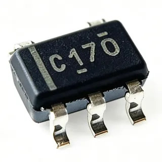
SN74LV1T125DBVR - 1-Bit Buffer/Level Shifter SOT-23-5 | TI
部品番号: SN74LV1T125DBVR ✓ 生産中| 数量 | 単価 | 小計 |
|---|---|---|
| 1 | $0.41 | $0.41 |
| 10 | $0.36 | $3.60 |
| 100 | $0.27 | $27.00 |
| 500 | $0.21 | $105.00 |
| 1,000 | $0.17 | $170.00 |
| 3,000 | $0.13 | $390.00 |
SN74LV1T125DBVR 概要
A logic level shifter is an integrated circuit that translates signals between circuits operating at different voltage domains, such as a 3.3 V microcontroller interfacing with a 1.8 V sensor. The SN74LV1T125 belongs to TI's LV1T family of single-gate CMOS logic with reduced input thresholds, sitting within the broader hierarchy of buffer/driver -> logic gate -> standard logic IC -> semiconductor. Its wide-input tolerance eliminates the need for external pull-ups or level-shift circuits in mixed-voltage designs, simplifying PCB layout and reducing BOM cost.
Key differentiating features include 5 V tolerant inputs that enable down-translation (e.g., 3.3 V input to 2.5 V output at VCC = 2.5 V), schmitt-trigger inputs for slow or noisy edges, low Ioff (partial-power-down support) for live-insertion scenarios, and ±8 mA balanced output drive. Typical propagation delay is around 3 to 5 ns at 5 V, suitable for moderate-speed control and data paths rather than high-speed SERDES interfaces.
Architecturally, the device uses a standard CMOS buffer topology with a 3-state output stage. The OE-bar input gates the output enable line directly to the output PMOS/NMOS pair; when OE is high, both output transistors are off and the pin presents high impedance. The reduced input-threshold design lets a 1.8 V input reliably switch a 5 V VCC rail, which simplifies system design when interfacing legacy 5 V peripherals with modern low-voltage controllers.
Typical applications include GPIO expansion on low-voltage MCUs, voltage translation between 1.8 V, 2.5 V, 3.3 V, and 5 V logic domains, signal buffering on long PCB traces or cables, bus isolation between multiple processors, and reset or enable signal distribution. Designers favor it for cost- and space-constrained designs that need a true single-gate solution without paying for an unused quad buffer.
When designing with this part, ensure that the OE pin is driven to a valid logic level (never left floating) because an undriven enable can cause shoot-through or undefined output states. Decouple VCC with a 100 nF ceramic capacitor placed within a few millimeters of the supply pin, and remember that partial-power-down (Ioff) only protects the output when VCC = 0 V; inputs above VCC will still forward-bias protection diodes if VCC is present.
This page synthesizes distributor pricing, drop-in alternatives, and practical design notes not found in the manufacturer datasheet alone, helping engineers quickly evaluate the SN74LV1T125DBVR for new designs and second-source strategies.
ドロップイン代替品: SN74LV1T125DBVR — 同一パッケージでピン互換。PCBの作り直しが必要な異なるパッケージの部品は除外されています。
このシリーズのバリエーション
同一シリーズでドロップイン互換のモデル: SN74LV1T125DBVR (同一形状・フットプリント) — 相違点: Function, Logic Family, MSL Level, Operating Temperature, Output Type.
クイック比較ツール — 並列比較する代替部品を選択:
SN74LV1T125DCKR
✅ ドロップイン ⚠️ 仕様未検証📋 参考代替品(カタログ未掲載)
SN74LVC1G125DBVR
✅ ドロップイン✓ 在庫あり
$0.13 / 個
データシートを見る →SN74LV1T126DBVR
✅ ドロップイン📋 参考代替品(カタログ未掲載)
74LV1T125GW
✅ ドロップイン📋 参考代替品(カタログ未掲載)
NL17SZ125DFT2G
✅ ドロップイン📋 参考代替品(カタログ未掲載)
XC7SET125GW
✅ ドロップイン📋 参考代替品(カタログ未掲載)
SN74LV1T125DBVR 最大定格&電気的特性
| 機能 | Single Buffer / Non-Inverting Gate |
| Logic Family | LV1T (CMOS, reduced threshold) |
| Number of Bits per Element | 1 |
| Number of Elements | 1 |
| 出力タイプ | 3-State (active-low OE) |
| VCC Range | 1.8 V to 5.5 V |
| Input Voltage Tolerance | Up to 5.5 V (independent of VCC) |
| Output Drive (IOH/IOL) | ±8 mA at VCC = 5 V |
| Ioff (Partial-Power-Down) | Supported |
| 動作温度 | -40 C to +125 C |
| パッケージ | SOT-23-5 (DBV) |
| 実装タイプ | Surface Mount |
| MSLレベル | 1 (per verified data) |
| RoHS ステータス | Compliant |
| Lead-Free | Yes |
SN74LV1T125DBVR ピン構成
| ピン 1 | OE — Output Enable, active LOW (high = high-Z output) |
| ピン 2 | A — Data input |
| ピン 3 | GND — Ground |
| ピン 4 | Y — 3-state data output |
| ピン 5 | VCC — Supply voltage (1.8 V to 5.5 V) |
主な用途
SN74LV1T125DBVR の用途: 6 件s: Mixed-Voltage GPIO Level Translation, Single-Line Signal Buffering on Long Traces, Reset and Enable Signal Distribution, Industrial Control and Automation, Portable and Battery-Powered Devices, Test and Measurement Equipment.
Mixed-Voltage GPIO Level Translation
The SN74LV1T125DBVR is widely used to translate signals between 1.8 V, 2.5 V, 3.3 V, and 5 V logic domains, such as connecting a 1.8 V sensor to a 3.3 V MCU. Its 5 V tolerant inputs and 1.8-5.5 V VCC range let a single part handle down-translation (3.3 V to 2.5 V at VCC = 2.5 V) without external pull-ups. The 3-state OE enables bidirectional bus sharing between two controllers, and the ±8 mA drive comfortably handles typical GPIO loads. Per TI's datasheet, this part reduces BOM count by replacing discrete resistor-divider level shifters in cost-sensitive designs.
おすすめ
Single-Line Signal Buffering on Long Traces
For board-to-board or cable-driven single-ended signals, the SN74LV1T125DBVR provides a clean CMOS buffer that restores logic levels on long PCB traces or backplane connections. Its ±8 mA drive handles capacitive loads that would otherwise slow down MCU GPIO edges, and the SOT-23-5 footprint fits easily near connectors. The 3-state output allows the signal to be disconnected for diagnostics or bus sharing. According to TI's design guidance, the LV1T family reduces transmission-line ringing on traces over 50 mm by providing a controlled-impedance driver.
おすすめ
Reset and Enable Signal Distribution
The SN74LV1T125DBVR is commonly used to fan out a single reset or enable signal to multiple ICs while isolating the source with its 3-state OE. This prevents back-driving issues when subsystems are powered down and allows orderly power-up sequencing. Its 1.8-5.5 V VCC compatibility means the same buffer IC works across mixed-voltage subsystems (e.g., 1.8 V SoC + 3.3 V peripheral). The Ioff feature ensures no leakage paths when VCC = 0, making it suitable for hot-swap or live-insertion cards.
おすすめ
Industrial Control and Automation
In industrial PLC and sensor-interface modules, the SN74LV1T125DBVR buffers 24 V-to-3.3 V translated logic signals between optocouplers and a low-voltage MCU. The -40 C to +125 C operating range handles factory-floor temperature extremes, while the SOT-23-5 package is robust enough for conformal-coated boards. According to TI's industrial portfolio documentation, single-gate LV1T devices are preferred in distributed I/O designs where PCB space is at a premium and channel count is low.
おすすめ
Portable and Battery-Powered Devices
The SN74LV1T125DBVR is well-suited for battery-powered wearables and portable instruments that must interface 1.8 V sensors with 3.3 V MCUs. Its low quiescent current and partial-power-down Ioff feature prevent leakage when the device is unpowered, extending battery life. The wide VCC range allows a single buffer to operate directly from a lithium-ion cell (2.7-4.2 V) without an additional regulator. Per TI's portable-design collateral, single-gate buffers are recommended in energy-harvesting designs where every microamp counts.
おすすめ
Test and Measurement Equipment
In bench instruments and data-acquisition modules, the SN74LV1T125DBVR provides level translation between legacy 5 V test circuitry and modern 3.3 V FPGAs or processors. Its fast propagation delay (typically 3-5 ns at 5 V) preserves signal integrity in measurement paths, and the 3-state output allows the FPGA to disconnect from the bus during calibration. The SOT-23-5 package integrates easily into dense probe-station PCBs. TI application notes recommend LV1T buffers for instrumentation requiring wide-input tolerance and predictable output drive.
おすすめ
おすすめ製品の概要
エンジニアリング参考データ: SN74LV1T125DBVR — 比較、設計ガイダンス、コンプライアンス情報。
選定ガイド
代替品との比較
| パラメータ | この製品 | SN74LVC1G125DBVR | SN74LV1T126DBVR | 74LV1T125GW | NL17SZ125DFT2G | XC7SET125GW |
|---|---|---|---|---|---|---|
| Brand | Texas Instruments | Texas Instruments | Texas Instruments | Nexperia | onsemi | Nexperia |
| Package | SOT-23-5 (DBV) | SOT-23-5 (DBV) - same | SOT-23-5 (DBV) - same | SOT-23-5 - same | SOT-23-5 - same | SOT-23-5 - same |
| VCC Range | 1.8 V to 5.5 V | 1.65 V to 5.5 V | 1.8 V to 5.5 V | 1.8 V to 5.5 V | 1.65 V to 5.5 V | 4.5 V to 5.5 V |
| Input Tolerance | 5.5 V tolerant | 5.5 V tolerant | 5.5 V tolerant | 5.5 V tolerant | 5.5 V tolerant | 5.5 V tolerant |
| OE Polarity | Active-Low (OE-bar) | Active-Low | Active-High (inverted) | Active-Low | Active-High | Active-Low |
| Output Drive (5 V) | ±8 mA | ±32 mA | ±8 mA | ±8 mA | ±32 mA | ±8 mA |
| Operating Temperature | -40 C to +125 C | -40 C to +125 C | -40 C to +125 C | -40 C to +125 C | -40 C to +125 C | -40 C to +85 C |
| Unit Price (qty 1) | $0.41 | $0.30 | $0.41 | $0.38 | $0.35 | $0.30 |
主な差別化要因
- Reduced input threshold for true 1.8 V-to-5 V translation (vs SN74LVC1G125DBVR)
- 5 V input tolerance independent of VCC (vs SN74LV1T126DBVR)
- Cross-brand second-source availability (vs 74LV1T125GW (Nexperia))
設計ノート
Estimated: At VCC = 3.3 V and ±8 mA continuous output drive, the SN74LV1T125DBVR draws less than 1 mA quiescent current and dissipates under 30 mW worst case. A 100 nF X7R decoupling capacitor placed within 5 mm of the VCC pin is sufficient for typical logic-edge transitions. For systems with high dI/dt on adjacent output lines, add a bulk 1-10 uF tantalum or ceramic capacitor near the supply rail to suppress ground bounce.
Never leave the OE pin floating; tie it to GND (for always-enabled) or to a controller GPIO with a defined logic level. A floating OE can cause shoot-through in the 3-state output stage, increasing quiescent current and producing undefined logic levels on Y. Also note that the Ioff feature only blocks output leakage when VCC = 0 V; if the input is driven above VCC while VCC is present, the internal ESD diodes may conduct.
Place the SOT-23-5 footprint with pin 1 dot/orientation matching TI's recommended land pattern (IPC-7351 nominal). Keep the input trace and output trace separated to minimize feedback through the package substrate. For high-speed (>10 MHz) applications, use a continuous ground plane under the IC to provide a low-impedance return path. If using the part for cable driving, add a series 33 ohm resistor near the output to dampen transmission-line ringing.
コンプライアンス情報
RoHS compliant per TI product page; MSL 1; not AEC-Q100 qualified (industrial/consumer use only).