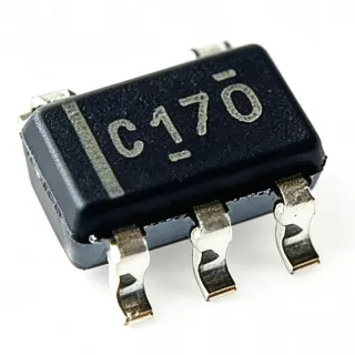
SN74LVC1G125DBVR - 1.65-5.5V 3-State Buffer Gate | TI | SOT-23-5
MPN: SN74LVC1G125DBVR ✓ Active| Qty | Unit Price | Extended |
|---|---|---|
| 1 | $0.41 | $0.41 |
| 10 | $0.36 | $3.60 |
| 100 | $0.29 | $29.00 |
| 500 | $0.22 | $110.00 |
| 1,000 | $0.17 | $170.00 |
| 3,000 | $0.13 | $390.00 |
SN74LVC1G125DBVR Overview
What is a bus buffer gate? A bus buffer gate is a digital logic primitive that isolates or buffers a single signal line, providing a high-impedance output when disabled so several devices can share a common bus without contention. The SN74LVC1G125 belongs to TI's LVC (Low-Voltage CMOS) logic family, which sits inside the broader CMOS logic IC category and balances low static power with fast switching at supply voltages from 1.8 V to 5 V.
Key features include an Ioff circuitry that prevents back-feeding current through the output when the part is partially powered down (a must for hot-swap and multi-rail designs), plus +/-24-mA balanced output drive at 3.3 V that lets one buffer directly drive multiple CMOS or TTL loads. Maximum ICC is only 10 uA, suiting battery-powered designs.
The CMOS architecture delivers low static power and high noise margin; the 1.65-V to 5.5-V range supports level buffering between 1.8-V and 3.3-V domains, 3.3-V to 5-V interfaces, and pure 5-V rails. Per the TI datasheet, the device can drive capacitive loads up to 50 pF while meeting all datasheet specifications; TI recommends a series resistor between the output and any load exceeding 50 pF to limit surge current.
Typical applications include logic level shifting between mixed-voltage rails, bus isolation in multi-board embedded systems, signal buffering for industrial control and PLC I/O, consumer electronics, and communication interfaces such as I2C, SPI, and UART lines. The SOT-23-5 footprint is also friendly to handheld and wearable designs where board area is at a premium.
When designing, ensure the OE pin is tied to a defined logic level - never floating - to avoid unwanted high-Z or contention. For loads above 50 pF, add a small series resistor to limit inrush per datasheet guidance. The part operates from -40C to +125C and starts around $0.41 at single-unit quantities (as of 2026-10-10).
This page synthesizes distributor pricing, drop-in alternatives, and practical design notes not found in the manufacturer datasheet.
Drop-in alternatives for SN74LVC1G125DBVR — same package, pin-to-pin compatible. Different-package parts requiring PCB rework are excluded.
Variants in this series
Same-series models that are drop-in compatible with SN74LVC1G125DBVR (same form factor and footprint) — differing in Output Type, Function, Operating Temperature, Package, MSL Level.
Quick Comparison Tool — Select alternative parts for side-by-side comparison:
SN74LVC1G125DBVT
✅ Drop-In📋 Reference alternative (not in catalog)
SN74LVC1G125QDBVRQ1
✅ Drop-In✓ In Stock
$0.11 / Unit
View Datasheet →SN74LVC1G17QDBVRQ1
✅ Drop-In✓ In Stock
$0.09 / Unit
View Datasheet →NC7SZ125P5X
✅ Drop-In📋 Reference alternative (not in catalog)
NC7SV125P5X
✅ Drop-In✓ In Stock
$0.15 / Unit
View Datasheet →SN74LVC1G07DBVR
✅ Drop-In ⚠️ Specs Unverified✓ In Stock
$0.19 / Unit
View Datasheet →SN74LVC1G125DBVR Maximum Ratings & Electrical Characteristics
| Function | Single non-inverting buffer / line driver |
| Logic Family | LVC (Low-Voltage CMOS) |
| Number of Elements | 1 |
| Bits per Element | 1 |
| Output Type | 3-State |
| Supply Voltage (VCC) | 1.65 V to 5.5 V |
| Input Voltage Tolerance | Up to 5.5 V (independent of VCC) |
| Maximum Quiescent Current (ICC) | 10 uA |
| Output Drive (IOUT) | +/-24 mA at 3.3 V |
| Output Enable | Active-low OE (high = Hi-Z) |
| Ioff / Partial-Power-Down | Supported |
| Propagation Delay (tpd) | Specified at 3.3 V (see datasheet) |
| Operating Temperature | -40C to +125C |
| Package | SOT-23-5 (DBV) |
| Mounting Type | Surface Mount |
| MSL Level | 1 (260C, unlimited) |
| RoHS Status | ROHS3 Compliant |
SN74LVC1G125DBVR Pin Configuration
| Pin 1 | OE — Output Enable (active low; high = Hi-Z) |
| Pin 2 | A — Data input |
| Pin 3 | GND — Ground |
| Pin 4 | Y — Data output (3-state) |
| Pin 5 | VCC — Supply voltage (1.65 V to 5.5 V) |
Typical Applications
SN74LVC1G125DBVR is suitable for 6 applications: Logic Level Shifting (1.8 V to 3.3 V or 3.3 V to 5 V), Bus Isolation in Multi-Board Embedded Systems, Signal Buffering for Industrial Control and PLC I/O, Consumer and Wearable Electronics, Communication Interface Buffers (UART, SPI, GPIO Expansion), Test and Measurement Front-Ends.
Logic Level Shifting (1.8 V to 3.3 V or 3.3 V to 5 V)
The SN74LVC1G125DBVR is well suited to unidirectional level shifting between mixed-voltage rails: with VCC at 5 V the input pins can be driven directly from a 1.8 V or 3.3 V CMOS GPIO (well within the 5.5 V input tolerance), and the output swings to the full 5 V CMOS rail. The Ioff feature prevents back-feed current if a downstream rail collapses before the upstream side, which protects the host MCU during power sequencing anomalies. Engineers routinely select this part where one-way voltage translation is needed between two domains without using a dedicated level translator like the SN74AVC or LSF0102 families.
Recommended
Bus Isolation in Multi-Board Embedded Systems
In backplanes and modular systems where multiple cards drive a shared bus, the SN74LVC1G125DBVR can sit in front of each driver's bus pin to provide Hi-Z isolation through the OE pin. Driving the OE high during reset or card-disconnect windows prevents back-driving and lets the bus arbitrator hot-swap cards safely. The SOT-23-5 footprint fits one buffer per board edge in tight card geometries, and the +/-24 mA drive at 3.3 V can fan out several downstream CMOS loads.
Recommended
Signal Buffering for Industrial Control and PLC I/O
Industrial PLCs and process controllers route 24 V signals to 3.3 V or 5 V MCUs through opto-isolated or resistive interfaces, with the digital side often benefiting from a clean CMOS buffer to debounce and fan-out the post-isolation logic level. The SN74LVC1G125DBVR's wide 1.65-5.5 V VCC range suits both 3.3 V microcontrollers and 5 V legacy logic, while its -40C to +125C operating range tolerates typical industrial thermal environments. The 3-state OE pin simplifies safety-rated designs where outputs must be released to Hi-Z on fault conditions.
Recommended
Consumer and Wearable Electronics
In consumer wearables, sensor hubs, and small IoT devices, the SN74LVC1G125DBVR serves as a tiny one-bit buffer between an ultra-low-power MCU and peripherals such as displays, BLE modules, or sensors. The 10 uA maximum quiescent current keeps sleep-mode draw negligible, and the SOT-23-5 footprint is compact enough for designs where every square millimeter counts. Engineers use this part to level-shift a coin-cell-domain GPIO into the 3.3 V rail needed by the radio module, with Ioff preventing back-feed when the radio rail is off.
Recommended
Communication Interface Buffers (UART, SPI, GPIO Expansion)
For unidirectional UART TX, SPI MOSI, or GPIO expansion lines, the SN74LVC1G125DBVR provides a one-bit 3-state buffer that isolates a single MCU pin from a long trace or noisy connector. The OE pin can be tied low for permanent pass-through, or driven by the MCU to release the line for shared access (e.g., half-duplex handshaking). Its 50 pF drive capability per the datasheet makes it suitable for typical board-level traces; TI recommends adding a series resistor for capacitive loads above 50 pF.
Recommended
Test and Measurement Front-Ends
In oscilloscope front-ends, logic analyzers, and lab instrumentation, the SN74LVC1G125DBVR can sit between a test probe and measurement ASIC to provide a defined 3-state release path during calibration. The +/-24 mA drive at 3.3 V easily handles typical 50-ohm-terminated probes, while the 5.5 V input tolerance protects the buffer from accidental over-voltage on test points. Designers use the active-low OE pin to tri-state outputs during self-test routines, avoiding contention with the DUT power rails.
Recommended
Recommended Products Summary
Engineering reference data for SN74LVC1G125DBVR — comparison, design guidance, and compliance information.
Selection Guide
Comparison with Alternatives
| Parameter | This Product | SN74LVC1G125DBVT | SN74LVC1G125QDBVRQ1 | SN74LVC1G17QDBVRQ1 | NC7SZ125P5X | NC7SV125P5X |
|---|---|---|---|---|---|---|
| Brand | Texas Instruments | Texas Instruments | Texas Instruments | Texas Instruments | onsemi | onsemi |
| Package | SOT-23-5 (DBV) | SOT-23-5 (DBV) - same | SOT-23-5 (DBV) - same | SOT-23-5 (DBV) - same | SOT-23-5 (P5) - same footprint, different marking | SOT-23-5 (P5) - same footprint, different marking |
| Supply Voltage (VCC) | 1.65 V to 5.5 V | 1.65 V to 5.5 V | 1.65 V to 5.5 V | 1.65 V to 5.5 V | 1.65 V to 5.5 V | 0.9 V to 3.6 V (lower max!) |
| Quiescent Current (ICC max) | 10 uA | 10 uA | 10 uA | 10 uA | 10 uA | 0.9 uA (ultra-low) |
| Output Enable Polarity | Active-low OE | Active-low OE | Active-low OE | Always enabled (no OE on 1G17) | Active-low OE | Active-low OE |
| Input Type | Standard CMOS | Standard CMOS | Standard CMOS | Schmitt-trigger (hysteresis) | Standard CMOS | Standard CMOS |
| Automotive Grade (AEC-Q100) | Not qualified | Not qualified | Grade 1 qualified (Q1 suffix) | Grade 1 qualified (Q1 suffix) | Not qualified | Not qualified |
Key Differentiators
- Wider VCC and input voltage range vs NC7SV125P5X (vs NC7SV125P5X)
- Automotive grade variant available in same footprint (vs SN74LVC1G125QDBVRQ1)
- Same SOT-23-5 footprint as cross-brand onsemi parts (vs NC7SZ125P5X)
- Better than SN74LVC1G17QDBVRQ1 when standard CMOS input is preferred (vs SN74LVC1G17QDBVRQ1)
Design Notes
Never leave the OE pin floating - it must be tied to a defined logic level (typically GND via a resistor or driven by the MCU) to avoid unpredictable Hi-Z or active output behavior. Floating OE on a 3-state buffer can cause bus contention, intermittent failures, and excess current draw. For designs that require the buffer to be permanently enabled, OE should be hard-wired to GND through a 10 kohm or smaller pull-down resistor. If your downstream trace is left floating when OE is high, add a weak pull-up/pull-down to define the Hi-Z state per system design rules.
Per the TI datasheet, the device can drive capacitive loads up to 50 pF while meeting all datasheet specifications; for larger capacitive loads, add a small series resistor (typically 22-100 ohm) between the Y output and the load to limit inrush current and reduce ground-bounce noise. Place any decoupling capacitor on VCC (typically 0.1 uF) within 5 mm of the VCC pin, with a wide, short trace to GND. Keep the OE and input traces short to avoid glitches during fast edges above 100 MHz.
When using the SN74LVC1G125DBVR for level shifting, ensure that the input high-level voltage (VIH) of the destination rail is satisfied at the maximum VCC you apply. At 5 V VCC, the CMOS input threshold is approximately 0.7 x VCC = 3.5 V, which means 3.3 V CMOS signals must be confirmed to swing above 3.5 V - many 3.3 V GPIOs reach only 3.3 V out, which is below the threshold and may be misinterpreted as logic low. Use a TXS/TXB family part or an SN74AVC level translator for fully rail-to-rail level translation scenarios.
Compliance Information
ROHS3 compliant and lead-free per TI part data and LCSC listing; MSL Level-1 (260C, unlimited). AEC-Q100 Grade 1 qualified variant available as SN74LVC1G125QDBVRQ1. REACH and conflict-mineral status should be confirmed on the latest TI material declaration document.