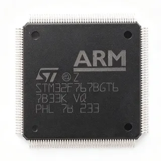
STM32F439BIT6 - 180MHz Cortex-M4 MCU 2MB Flash 208-LQFP
部品番号: STM32F439BIT6 ✓ 生産中| 数量 | 単価 | 小計 |
|---|---|---|
| 1 | $28.5 | $28.50 |
| 10 | $25.8 | $258.00 |
| 100 | $22.75 | $2,275.00 |
| 500 | $20.1 | $10,050.00 |
| 1,000 | $18.25 | $18,250.00 |
STM32F439BIT6 概要
A microcontroller (MCU) is a single-chip computer containing a CPU, memory, and programmable peripherals. The STM32 family by STMicroelectronics is one of the most widely deployed 32-bit microcontroller families worldwide, with the F4 series specifically targeting high-performance applications. In the broader taxonomy, the STM32F439BIT6 is an MCU (microcontroller unit) -> embedded processor -> semiconductor device. The Cortex-M4 architecture itself is a 32-bit RISC core designed for deterministic real-time control, while the M4 variant adds DSP and SIMD instructions as well as optional FPU for floating-point math.
Key differentiating specifications of the STM32F439BIT6 include 2 MB of Flash with 256+4 KB SRAM, three 12-bit ADCs (2.4 MSPS each), two 12-bit DACs, USB 2.0 OTG full-speed and high-speed, an Ethernet MAC (MII/RMII), three CAN 2.0B interfaces, six general-purpose timers plus two advanced-control timers, and an integrated TFT LCD controller. The cryptographics and hash acceleration blocks provide AES-128/192/256, SHA-1/SHA-2, and a true random number generator (TRNG) without burdening the CPU.
Architecturally, the device pairs the Cortex-M4 core with ST's proprietary ART Accelerator (Adaptive Real-Time memory accelerator) that allows 0-wait-state execution from Flash at full 180 MHz speed, eliminating the typical performance penalty of Flash-based MCUs. The multi-layer AHB/APB bus matrix and DMA controllers (two DMA controllers with 16 streams each) enable parallel data movement between peripherals and memory at high throughput, while the supply scheme (1.2 V core, 3.3 V I/O) is managed internally by voltage regulators.
Typical applications include industrial control HMIs with TFT displays, point-of-sale terminals, barcode scanners, smart energy meters, factory automation PLCs, automotive infotainment head units, medical monitoring equipment, and high-end consumer gateways. The combination of high-speed processing, large memory, and integrated peripherals makes the STM32F439BIT6 especially attractive for applications that would otherwise require an external controller plus separate memory chips.
When designing with this MCU, plan oscillator and decoupling layout carefully: place the 8 MHz HSE crystal (or resonator) within 5 mm of OSC_IN/OSC_OUT pins with dedicated ground and power traces, and route the 32.768 kHz LSE traces on a separate guarded layer to avoid jitter. Provide at least four 100 nF decoupling capacitors within a few millimeters of the VDD pins, plus a bulk capacitor near each VDD/VSS pair. This page synthesizes distributor pricing, drop-in alternatives, and practical design notes not found on a single competitor or distributor listing.
ドロップイン代替品: STM32F439BIT6 — 同一パッケージでピン互換。PCBの作り直しが必要な異なるパッケージの部品は除外されています。
このシリーズのバリエーション
同一シリーズでドロップイン互換のモデル: STM32F439BIT6 (同一形状・フットプリント) — 相違点: ADC, DMIPS, Package, SRAM, Mounting Type.
クイック比較ツール — 並列比較する代替部品を選択:
STM32F429BIT6
✅ ドロップイン ⚠️ 仕様未検証✓ 在庫あり
$11.05 / 個
データシートを見る →STM32F437BIT6
✅ ドロップイン ⚠️ 仕様未検証📋 参考代替品(カタログ未掲載)
STM32F439BIT6 最大定格&電気的特性
| Core Architecture | ARM Cortex-M4 with FPU and DSP instructions |
| 最大クロック周波数 | 180 MHz |
| DMIPS | 225 DMIPS |
| Program Memory (Flash) | 2 MB (2M x 8) |
| SRAM | 256 KB + 4 KB CCM |
| Operating Voltage Range | 1.8 V to 3.6 V |
| パッケージ | 208-LQFP (28x28 mm) |
| ピン数 | 208 pins |
| 動作温度範囲 | -40 C to +85 C |
| ADC | 3 x 12-bit, 2.4 MSPS (up to 24 channels) |
| DAC | 2 x 12-bit |
| Timers | 12 (general-purpose, advanced-control, basic) |
| Communication Interfaces | USB OTG FS + HS, Ethernet MAC, 3x CAN, 6x USART, 4x SPI, 3x I2C |
| Cryptographic Acceleration | AES-128/192/256, SHA-1/SHA-2, TRNG |
| LCD-TFT Controller | Yes (up to XGA resolution) |
| DMA Controllers | 2 x DMA, 16 streams each |
| 実装タイプ | Surface Mount |
| RoHS ステータス | Compliant |
STM32F439BIT6 208-lqfp (28x28 mm) ピン配置ガイド
STM32F439BIT6 (208-lqfp (28x28 mm) パッケージ) のピン配置。 このデジタルICには、GPIO、通信インターフェース (UART、SPI、I2C)、および電源ピンが含まれています。代替ピン機能と設定オプションについては、メーカーのデータシートを参照してください。組み込みシステム設計とPCBレイアウトに不可欠です。

詳細なピン配置データはありません: STM32F439BIT6.
詳細は データシート をご参照ください。
主な用途
STM32F439BIT6 の用途: 6 件s: Industrial HMI with TFT Display, Point-of-Sale Terminal, Smart Energy Meter, Barcode Scanner / Data Terminal, Medical Patient Monitor, Factory Automation PLC / Industrial Gateway.
Industrial HMI with TFT Display
The STM32F439BIT6 is well suited for industrial Human-Machine Interface (HMI) with integrated color TFT panels. Its integrated LCD-TFT controller drives displays up to XGA resolution without an external graphics controller, while the 180 MHz Cortex-M4 core delivers 225 DMIPS to manage touch-input handling, real-time data acquisition from sensors over CAN, and dynamic graphical updates. The crypto block (AES-128/192/256, SHA-1/SHA-2) protects operator authentication and signed firmware, and 2 MB Flash stores large bitmap assets and multi-language GUIs. The 256 KB SRAM is sufficient for framebuffers and touch-event queues, while the Ethernet MAC supports remote maintenance over industrial networks.
おすすめ
Point-of-Sale Terminal
POS terminals benefit from the STM32F439BIT6's combined cryptography, USB OTG high-speed, and Ethernet MAC in a single chip. The Cortex-M4 handles payment-protocol stacks (EMV, NFC peer transactions) while hardware AES accelerates TLS handshake and TRNG provides entropy for key generation required by PCI PTS. USB OTG HS connects to printer peripherals and barcode scanners, while Ethernet and three CAN buses integrate with cash drawers and inventory systems. The 2 MB Flash stores EMV Level 1/2 firmware and merchant-specific configuration, and ST's cryptographic libraries are certified for payment applications.
おすすめ
Smart Energy Meter
The STM32F439BIT6 powers three-phase smart energy meters with its 180 MHz performance, three simultaneous 12-bit 2.4 MSPS ADCs for voltage and current sensing, and hardware crypto for secure DLMS/COSEM communication. The Cortex-M4 with FPU executes DSP-based harmonic analysis and power-quality algorithms in real time. RTC with calendar, four 16-bit timers plus advanced-control timers drive metrology calculations and tamper detection, while the integrated LCD controller drives segmented or matrix displays. 2 MB Flash fits DLMS stacks, calibration tables, and event logs, while 256 KB SRAM holds metering buffers, and Ethernet or PLC connectivity enables AMI backhaul.
おすすめ
Barcode Scanner / Data Terminal
Industrial barcode scanners and data terminals use the STM32F439BIT6 to process image streams from CMOS sensors, perform OCR/decode locally, and connect via USB OTG, Bluetooth, or Wi-Fi modules. The ART Accelerator allows 0-wait-state execution at full 180 MHz for compressed JPEG decoding and barcode recognition, while 256 KB SRAM provides buffer space for image preprocessing before streaming over Ethernet. Hardware AES-128/192/256 protects scanned data in transit and at rest, USB OTG HS handles high-speed connectivity, and the 208-LQFP package supports the I/O count needed for keypad, display, and multiple wireless interfaces.
おすすめ
Medical Patient Monitor
Patient-monitoring devices leverage the STM32F439BIT6's high-performance DSP capability, large memory, and integrated security for multi-parameter vital-sign processing. The single-precision FPU runs DSP filter chains (FFT, FIR, IIR) for ECG, SpO2, and respiration analysis with deterministic 180 MHz timing. The three 12-bit ADCs simultaneously sample multiple biosensor channels; hardware AES safeguards PHI in transit and at rest, and the 2 MB Flash plus 256 KB SRAM support waveform buffers and trend storage. The USB OTG HS port streams continuous waveforms to host PCs while Ethernet MAC enables HL7 integration.
おすすめ
Factory Automation PLC / Industrial Gateway
Factory automation PLCs and industrial gateways benefit from the STM32F439BIT6's triple CAN 2.0B interface, Ethernet MAC for PROFINET/EtherCAT/IP, USB OTG for programming ports, and 180 MHz Cortex-M4 cycle budget for executing complex motion-control or PLC logic. Hardware AES and SHA accelerators secure machine-to-machine (M2M) communications against industrial cyber threats, while the LCD-TFT controller drives HMI panels on the machine directly. ST's IEC 61508 and IEC 62443 documentation packages support safety and security certifications for industrial automation deployments requiring 2 MB Flash for protocol stacks.
おすすめ
おすすめ製品の概要
エンジニアリング参考データ: STM32F439BIT6 — 比較、設計ガイダンス、コンプライアンス情報。
選定ガイド
代替品との比較
| パラメータ | この製品 | STM32F429BIT6 | STM32F437BIT6 | GD32F450VET6 |
|---|---|---|---|---|
| Brand | STMicroelectronics | STMicroelectronics | STMicroelectronics | GigaDevice |
| Package | 208-LQFP (28x28 mm) | 208-LQFP (28x28 mm) | 208-LQFP (28x28 mm) | 100-LQFP (different) |
| Core Architecture | ARM Cortex-M4 with FPU + DSP | ARM Cortex-M4 with FPU + DSP | ARM Cortex-M4 with FPU + DSP | ARM Cortex-M4 with FPU |
| Maximum Clock Frequency | 180 MHz | 180 MHz | 180 MHz | 200 MHz |
| Flash Memory | 2 MB | 2 MB | 1 MB | 3 MB |
| SRAM | 256 KB + 4 KB CCM | 256 KB + 4 KB CCM | 256 KB + 4 KB CCM | 256 KB + 16 KB CCM |
| Cryptographic Accelerator | AES-128/192/256, SHA, TRNG | None | AES-128/192/256, SHA, TRNG | None (software library only) |
| Ethernet MAC | 10/100 MII/RMII | 10/100 MII/RMII | 10/100 MII/RMII | 10/100 MII/RMII |
| USB OTG | FS + HS (ULPI) | FS + HS (ULPI) | FS + HS (ULPI) | FS + HS (ULPI) |
| Unit Price (qty 100) | $22.75 | $18-22 (estimated, no crypto) | $16-19 (smaller Flash) | $8-12 (estimated, cross-brand) |
主な差別化要因
- Hardware Cryptographic Acceleration Block (AES/SHA/TRNG) (vs STM32F429BIT6)
- Double the Flash vs STM32F437 Family (vs STM32F437BIT6)
- Mature ST Ecosystem and Toolchain Support (vs GD32F450 (GigaDevice))
設計ノート
The 208-LQFP at 28x28 mm with 0.5 mm lead pitch requires a 4-layer PCB minimum to keep impedance-controlled traces (for ULPI USB HS and Ethernet RMII) clean. Place the 8-25 MHz HSE crystal within 5 mm of OSC_IN/OSC_OUT pins, with a guard ring and dedicated ground via stitching every 5-10 mm. Keep the 32.768 kHz LSE crystal traces short and isolated from noisy digital lines. Place all VDD/VSS pairs with local 100 nF X7R ceramic decoupling capacitors within 1-3 mm, and at least one bulk 4.7 uF capacitor near each regulator output rail to handle switching transients.
Power sequencing: the STM32F439BIT6 has core (1.2 V) and I/O (3.3 V) supply domains that must ramp together. When using ST's internal voltage regulator (PDR_ON pin = VDD), ensure VDD is stable before the chip begins boot. For low-power STOP/STANDBY modes, use the integrated PVD (Programmable Voltage Detector) to wake the MCU when supply rises above the configured threshold. Estimated: at 180 MHz active current consumption is approximately 60-80 mA, while STOP mode drops to ~10 uA - size your LDO budget accordingly.
The LQFP208 at full 180 MHz core clock and active peripherals can dissipate up to ~1 W under sustained load. While LQFP has higher theta_JA than QFN packages (~28 C/W on 4-layer PCB versus ~15 C/W for similar QFN), the package can handle this dissipation without active cooling if ambient stays below 70 C. For continuous 180 MHz operation, verify that your PCB copper pour connects to a ground plane and provides adequate thermal dissipation. Estimated: at 25 C ambient and full load, junction temperature rises around 28 C above ambient - well within the 85 C commercial max.
The ULPI USB HS interface runs at 60 MHz with strict impedance requirements (90 ohm differential). Route DP/DM with 90-ohm differential impedance, length-matched to within 0.15 mm, and keep pairs away from clock edges by at least 3W. Ethernet RMII traces need 50-ohm single-ended impedance to the PHY; place series-termination resistors if your PHY recommends them. The ULPI bus to external HS PHY (such as USB3300) has a maximum total trace length of 50 mm with matched lengths.
Common pitfalls when designing with this MCU include: (1) Failing to enable the ART Accelerator prefetch buffer in startup code - this incurs 5+ wait states on Flash; (2) Floating unused GPIO pins - they should be configured as analog inputs with internal pull-down to avoid stray interrupts; (3) Misconfiguring the HSE bypass vs crystal mode - check boot pins BOOT0/BOOT1 for proper boot mode; (4) Forgetting to enable the IWDG and WWDG window watchdogs in safety-critical designs; (5) Not providing adequate wait states when using slow external memories on the FSMC bus at high speeds.
コンプライアンス情報
RoHS compliant per ST product page. Industrial temperature range -40C to +85C. Not AEC-Q100 qualified; this is an industrial-grade part. STMicroelectronics publishes IEC 61508 documentation for safety-related designs.