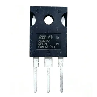
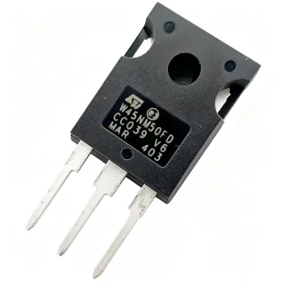
STW20N60M2 - 600V 20A N-Channel Power MOSFET | STMicroelectronics
部品番号: STW20N60M2 ✓ 生産中| 数量 | 単価 | 小計 |
|---|---|---|
| 1 | $3.25 | $3.25 |
| 10 | $2.92 | $29.20 |
| 100 | $2.6 | $260.00 |
| 500 | $2.34 | $1,170.00 |
| 1,000 | $2.08 | $2,080.00 |
STW20N60M2 概要
A Power MOSFET is a type of field-effect transistor optimized for switching and amplification of power. It operates by controlling the conductivity between the drain and source terminals through an insulated gate voltage. Power MOSFETs are essential components in power electronics, serving as switches in DC-DC converters, AC-DC power supplies, motor drives, and inverters. They are preferred for their fast switching speeds, high input impedance, and low drive power requirements compared to bipolar junction transistors.
Key features of the STW20N60M2 include a low gate charge (Qg) of 45 nC, which reduces switching losses and enables high-frequency operation. The device also offers a fast body diode with low reverse recovery charge, making it suitable for bridge topologies. The MDmesh M2 technology provides an excellent figure of merit (RDS(on) x Qg), balancing conduction and switching losses for optimal efficiency.
The STW20N60M2 utilizes a vertical DMOS structure with a striped layout, optimizing current distribution and thermal performance. The TO-247 package offers a low thermal resistance of 0.5°C/W (junction-to-case), allowing efficient heat dissipation. The device is avalanche-rated, with an avalanche energy of 1.2 J, ensuring robustness in inductive load switching.
Typical applications include switch-mode power supplies (SMPS), power factor correction (PFC) circuits, solar inverters, and motor drives. The high voltage rating and low on-resistance make it ideal for 400V bus systems and 3-phase rectification. In PFC boost converters, the low gate charge enables high switching frequencies, reducing magnetic component size.
When designing with this device, ensure proper gate drive voltage (typically 10V to 15V) to achieve low RDS(on). A gate resistor may be needed to control switching speed and reduce EMI. Adequate heatsinking is essential for continuous operation at high currents, as power dissipation can exceed 100W in worst-case conditions.
ドロップイン代替品: STW20N60M2 — 同一パッケージでピン互換。PCBの作り直しが必要な異なるパッケージの部品は除外されています。
クイック比較ツール — 並列比較する代替部品を選択:
STW20N60M2-EP
✅ ドロップイン ⚠️ 仕様未検証📋 参考代替品(カタログ未掲載)
STW20N60M2-1
✅ ドロップイン ⚠️ 仕様未検証📋 参考代替品(カタログ未掲載)
IPW60R099P7
✅ ドロップイン ⚠️ 仕様未検証📋 参考代替品(カタログ未掲載)
FCH20N60
✅ ドロップイン ⚠️ 仕様未検証📋 参考代替品(カタログ未掲載)
TK20A60W
✅ ドロップイン ⚠️ 仕様未検証📋 参考代替品(カタログ未掲載)
STW20N60M2 最大定格&電気的特性
| Technology | MDmesh M2 |
| Drain-Source Voltage (VDS) | 600 V |
| Continuous Drain Current (ID) | 20 A at 25°C |
| Pulsed Drain Current (IDM) | 60 A |
| On-Resistance (RDS(on)) | 0.19 ohm typical |
| Gate-Source Voltage (VGS) | ±25 V |
| Gate Charge (Qg) | 45 nC |
| Input Capacitance (Ciss) | 1900 pF |
| Output Capacitance (Coss) | 120 pF |
| Reverse Transfer Capacitance (Crss) | 10 pF |
| Avalanche Energy (EAS) | 1.2 J |
| 動作温度範囲 | -55°C to +150°C |
| パッケージ | TO-247 |
| 実装タイプ | Through Hole |
| RoHS ステータス | Compliant |
STW20N60M2 ピン構成
| ピン 1 | Gate — Gate drive input |
| ピン 2 | Drain — Drain connection |
| ピン 3 | Source — Source connection |
安全動作領域
主な用途
STW20N60M2 の用途: 6 件s: Switch-Mode Power Supplies (SMPS), Power Factor Correction (PFC), Solar Inverters, Motor Drives, Welding Equipment, Uninterruptible Power Supplies (UPS).
Switch-Mode Power Supplies (SMPS)
The STW20N60M2 is ideal for SMPS due to its 600V rating and low on-resistance. In a typical flyback or forward converter, the MOSFET switches at high frequency, and its low gate charge (45 nC) reduces switching losses. The low RDS(on) of 0.19 ohm minimizes conduction losses, improving overall efficiency. The TO-247 package allows efficient heat dissipation, enabling continuous operation at high power levels. Compared to lower-voltage MOSFETs, the 600V rating provides ample margin for voltage spikes in offline applications.
おすすめ
Power Factor Correction (PFC)
In boost PFC circuits, the STW20N60M2 operates at high switching frequencies to shape the input current waveform. Its low gate charge enables fast switching, reducing EMI and improving power factor. The device's avalanche ruggedness (1.2 J) ensures reliability during transient conditions. The 600V rating is suitable for universal input (85-265VAC) applications, where the boost output is typically 400V. The low on-resistance reduces conduction losses, which is critical for meeting efficiency standards like 80 PLUS.
おすすめ
Solar Inverters
The STW20N60M2 is used in solar inverter DC-DC boost stages and H-bridge inverters. Its high voltage rating (600V) handles the DC bus voltage from solar panels, which can reach 500V in series configurations. The low on-resistance minimizes losses, improving the overall efficiency of the inverter. The fast body diode reduces reverse recovery losses in bridge topologies. The TO-247 package allows for easy mounting on heatsinks, essential for outdoor installations where ambient temperatures can be high.
おすすめ
Motor Drives
In motor drive applications, the STW20N60M2 is used in the inverter stage to drive AC motors. Its 600V rating is suitable for 3-phase 400V systems. The low gate charge allows for high PWM frequencies, reducing motor noise and improving control accuracy. The avalanche energy rating ensures robustness during regenerative braking and inductive load switching. The device's low on-resistance reduces power dissipation, allowing for smaller heatsinks and more compact drive designs.
おすすめ
Welding Equipment
The STW20N60M2 is used in inverter-based welding machines, where it switches at high frequency to control the welding current. Its high voltage rating and low on-resistance enable efficient power transfer, reducing energy consumption. The device's ruggedness handles the harsh electrical environment of welding, including voltage spikes and high currents. The TO-247 package allows for effective cooling, ensuring reliable operation in continuous-duty welding applications.
おすすめ
Uninterruptible Power Supplies (UPS)
In UPS systems, the STW20N60M2 is used in the inverter and battery charger stages. Its 600V rating handles the DC bus voltage, and the low on-resistance ensures high efficiency, extending battery life. The fast switching capability reduces losses in high-frequency operation, allowing for smaller transformers and inductors. The device's reliability is critical for UPS applications, where downtime is unacceptable.
おすすめ
おすすめ製品の概要
エンジニアリング参考データ: STW20N60M2 — 比較、設計ガイダンス、コンプライアンス情報。
選定ガイド
代替品との比較
| パラメータ | この製品 | STW20N60M2-EP | IPW60R099P7 | FCH20N60 |
|---|---|---|---|---|
| Package | TO-247 | TO-247 | TO-247 | TO-247 |
| Brand | STMicroelectronics | STMicroelectronics | Infineon | onsemi |
| Drain-Source Voltage (VDS) | 600 V | 600 V | 600 V | 600 V |
| Continuous Drain Current (ID) | 20 A | 20 A | 20 A | 20 A |
| On-Resistance (RDS(on)) | 0.19 ohm | 0.19 ohm | 0.099 ohm | 0.19 ohm |
| Gate Charge (Qg) | 45 nC | 45 nC | 38 nC | 45 nC |
| Avalanche Energy (EAS) | 1.2 J | 1.5 J | 1.0 J | 1.0 J |
| Operating Temperature Range | -55°C to +150°C | -55°C to +150°C | -55°C to +150°C | -55°C to +150°C |
主な差別化要因
- Low on-resistance of 0.19 ohm (vs IPW60R099P7)
- High avalanche energy of 1.2 J (vs FCH20N60)
- MDmesh M2 technology (vs TK20A60W)
設計ノート
The STW20N60M2 can dissipate significant power in high-current applications. For example, at 20A and RDS(on) of 0.19 ohm, conduction losses are 76W. With a junction-to-case thermal resistance of 0.5°C/W, a heatsink with a thermal resistance of 0.5°C/W or better is required to keep the junction temperature below 150°C at 25°C ambient. Use thermal paste and proper mounting torque to ensure good thermal contact.
For TO-247 packages, ensure the leads are soldered with adequate copper area for heat sinking. The drain tab is electrically connected to the drain, so it may require isolation or connection to the appropriate node. Place gate drive components close to the gate pin to minimize parasitic inductance. Use a gate resistor (e.g., 10 ohm) to control switching speed and reduce EMI.
Do not exceed the maximum gate-source voltage of ±25V. Ensure the gate drive voltage is sufficient to fully enhance the MOSFET (typically 10V to 15V). Avoid operating in the linear region for extended periods, as this can cause excessive power dissipation. When paralleling devices, use separate gate resistors to prevent oscillations.
コンプライアンス情報
RoHS compliant per STMicroelectronics. Not AEC-Q100 qualified as it is not an automotive-grade part.