The C8051F061 is an 8-bit mixed-signal microcontroller from Silicon Labs that runs its 8051-compatible core at up to 25 MHz (25 MIPS peak), integrates 64 KB of in-system-programmable flash and 4.25K x 8 bits of RAM, and combines a 16-bit single-channel 1 Msps ADC, an eight-channel 10-bit ADC, a 12-bit two-channel DAC, and three analog comparators in a 64-TQFP (10 x 10 mm) surface-mount package. It operates from a 2.7 V to 3.6 V supply and provides SPI, SMBus, I2C, two UARTs, and CAN 2.0B. XAIPART lists 16,800 units in stock with MOQ 1 as of 2026-11-02; tiered pricing starts at $64.6875 for single units and drops to $37.7344 at 1,000 pieces as of 2026-11-02. The part carries an active lifecycle status. This guide consolidates verified specifications, design-in guidance, same-family alternatives, and sourcing data so you can evaluate the C8051F061 for industrial sensing, process control, data acquisition, and CAN-connected instrumentation in one place, and cross-check every number on the C8051F061 product page or in the broader component catalog.
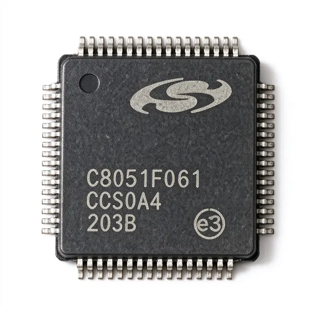
What Is the C8051F061 and Why Does Its Mixed-Signal Integration Matter?
A mixed-signal microcontroller integrates digital processing with analog conversion and comparison functions on one die. The C8051F061, a member of Silicon Labs' C8051F06x family, pairs an 8051-compatible core with on-chip ADC, DAC, comparator, timer, serial-interface, and CAN resources. The practical consequence: a board that measures analog signals, generates control voltages, and talks to a CAN or UART network can be built around one 64-pin device instead of a separate MCU, ADC, DAC, and comparator chain.
The verified specification set divides into three subsystems:
- Digital core: 25 MHz maximum clock, 25 MIPS peak throughput, 64 KB flash, 4.25K x 8 RAM, 24 digital I/O lines, five timers, a watchdog timer, and the Programmable Counter Array.
- Analog subsystem: a 16-bit, one-channel ADC sampling at 1 Msps; an eight-channel 10-bit ADC; a 12-bit, two-channel DAC; three analog comparators; and an on-chip temperature sensor.
- Communication: SPI, SMBus, I2C, two UARTs, and CAN 2.0B.
The 24-I/O allocation is a defining family characteristic. Within C8051F06x, devices split into a 59-I/O group (F060, F062, F064, F066) and a 24-I/O group (F061, F063, F065, F067). That is a 35-line difference, so it drives package selection, PCB routing, and firmware peripheral mapping before any other specification matters.
Takeaway: Shortlist the C8051F061 when your design needs high-resolution single-channel acquisition plus multichannel lower-resolution monitoring, at least two serial links, and CAN, without exceeding 24 digital I/O lines.
How Do You Design In the C8051F061 Correctly?
Treat the supply range as the first hard constraint. The verified operating window is 2.7 V to 3.6 V, so design around a regulated 3.3 V rail and confirm that no supply transient pushes the part above 3.6 V. The limit applies to both the digital core and the integrated analog resources, which share the supply. Place decoupling capacitors close to the device pins.
Analog layout is the second constraint. Because the ADC, DAC, and comparators share the die with a 25 MHz digital core, analog inputs, high-impedance nodes, and ground returns need deliberate routing. Keep analog traces away from switching nodes and digital return currents; preserve a clean analog ground structure; and decouple locally at the package. These steps directly protect the 16-bit ADC's usable resolution, since digital noise coupled into a high-resolution converter consumes effective bits faster than any specification margin can absorb.
On the firmware side, plan resource assignment before schematic freeze:
- Use the 16-bit, 1-channel ADC for the single most demanding measurement, and distribute slower channels across the eight-channel 10-bit ADC.
- Assign the two 12-bit DAC channels to actuator commands or calibration/excitation outputs.
- Use the three comparators for fast threshold detection that must not wait on software.
- Split communication roles across the two UARTs (for example, console plus peripheral), SPI for a higher-speed local bus, I2C/SMBus for sensors and configuration devices, and CAN 2.0B for the industrial network.
- Enable the watchdog timer and size communications queues within the 4.25K x 8 RAM budget.
Pin-level design must use the official family document. The complete numbered pin table and analog/alternate-function assignments for the 64-TQFP footprint are published in the Silicon Laboratories C8051F06x datasheet; this article does not reproduce pin-level tables, so download the datasheet and use the package-specific pin table for land-pattern and pin-multiplexing work. Verify peripheral multiplexing for the exact variant you order rather than assuming every C8051F06x member has identical resources.
Takeaway: Freeze a 3.3 V rail, ring the package with local decoupling, route analog away from digital returns, and pull your pin map from the official datasheet before starting layout.
What Design Decisions Follow From the Verified Specifications?
Consider a representative build: a compact process-control node that reads one precision process variable, monitors several auxiliary sensors, drives one actuator, and reports over CAN. The C8051F061 covers the whole chain in one package.
- Acquisition budget: the 16-bit ADC samples at 1 Msps, so a 10 kHz control loop can oversample heavily and average down noise while leaving CPU headroom on the 25 MIPS core.
- Auxiliary monitoring: the eight-channel 10-bit ADC handles slower auxiliary inputs; 10-bit resolution over the ADC's input range is adequate for supervision channels that do not need precision.
- Actuation: one of the two 12-bit DAC channels generates the actuator command. With 12 bits, the commanded output resolves to 1/4096 of full scale, sufficient for most analog actuator interfaces; reserve the second DAC channel for a calibration or reference signal.
- Protection: comparators provide hardware-level threshold detection independent of firmware latency, and the watchdog timer recovers the node from software faults.
- Memory sizing: 64 KB flash accommodates control logic plus a CAN and UART protocol stack; 4.25K x 8 RAM must hold communications buffers, so size CAN and UART FIFO depths against that budget before adding features.
The one judgment call the specifications cannot settle is thermal accuracy: the on-chip temperature sensor supports local thermal supervision, but on-chip readings are influenced by package dissipation and PCB thermal paths. Calibrate and run a representative thermal test before using the sensor for safety-critical decisions.
Takeaway: Map your highest-value analog channel to the 16-bit ADC, budget RAM for CAN/UART buffering explicitly, and validate the internal temperature sensor empirically before trusting it in safety paths.
Which Alternatives Can Replace the C8051F061?
The verified cross-reference data identifies the C8051F067 as a same-family candidate: it shares the 24-I/O C8051F06x grouping and the 64-TQFP footprint, with analog and communications resources varying by variant, producing an estimated 90% parameter match. No cross-manufacturer drop-in equivalent is established by the available data; a functional substitute from another vendor would require hardware and firmware changes and cannot honestly be classified as drop-in.
Other family groupings matter for I/O-count decisions. C8051F060 sits in the 59-I/O group, so it fits designs needing more direct digital connections, while C8051F062 is a different member from C8051F061 and should not be assumed interchangeable: the two groups differ by 35 digital I/O lines.
| Parameter | C8051F061 | C8051F067 |
|---|---|---|
| Family / I/O grouping | C8051F06x, 24-I/O group | C8051F06x, 24-I/O group |
| Package | 64-TQFP (10 x 10 mm) | 64-TQFP footprint |
| Core / clock | 8051-compatible, 25 MHz, 25 MIPS | Per-variant; see family datasheet |
| Flash / RAM | 64 KB flash, 4.25K x 8 RAM | Per-variant; see family datasheet |
| Analog resources | 16-bit 1-ch 1 Msps ADC; 8-ch 10-bit ADC; 12-bit 2-ch DAC; 3 comparators | Per-variant; analog resources vary |
| Serial interfaces | SPI, SMBus, I2C, 2 UARTs, CAN 2.0B | Per-variant; communications resources vary |
| Estimated parameter match | — | 90% (estimated) |
Before substituting, validate every candidate against the official pinout, clock requirements, memory map, and firmware dependencies in the C8051F06x datasheet. A 90% estimated match still leaves variant-specific differences in analog arrangement, peripheral multiplexing, and pin mapping that can break an otherwise footprint-compatible swap.
Takeaway: For footprint-oriented replacement, evaluate C8051F067 first; for more I/O, move to a 59-I/O family member such as C8051F060, and always re-verify pins and peripherals against the datasheet.
What Is the C8051F061's Market Position, Lifecycle Status, and Supply Situation?
The C8051F061 carries an active lifecycle status, so Silicon Labs continues to list it as a current product rather than one flagged for discontinuation. For long-lifetime industrial designs, active status is the primary sourcing signal, and it is the only lifecycle information the verified data provides; no end-of-life, last-time-buy, or replacement-program dates appear in the database.
Supply looks healthy on XAIPART: 16,800 units are in stock as of 2026-11-02 with a minimum order quantity of 1, which supports both prototype quantities and modest production runs without a factory lead-time wait. The verified database does not include a numerical manufacturer lead time or factory allocation data, so production planners should confirm current authorized-distributor quantity and the exact package suffix (the LCSC record references a C8051F061-GQ option) before committing a build.
Pricing data carries one conflict worth stating explicitly. XAIPART's verified tier table, as of 2026-11-02, lists $64.6875 at qty 1, $46.7188 at qty 10, $41.3281 at qty 100, $39.5313 at qty 500, and $37.7344 at qty 1000. Separately, a verified LCSC record for the C8051F061-GQ, as of 2026-10-30, shows a single-unit price of $49.2381 with the part in stock. These two sources disagree on single-unit pricing, and neither should be silently averaged with the other; request quotations for production quantities and confirm the exact package suffix, stock, and delivered price before ordering.
Takeaway: The part is active and well-stocked (16,800 units, MOQ 1 as of 2026-11-02), but the single-unit price conflict between sources means you should quote before you buy in volume.
What Should Buyers Watch Next for the C8051F061?
Anchor your watchlist to the verified specifications and sourcing facts rather than speculation:
- Stock depth: 16,800 units at MOQ 1 is comfortable today (as of 2026-11-02), but no factory lead-time number exists in the verified data. Re-check stock on the C8051F061 product page before each production release.
- Tier economics: the step from $64.6875 (qty 1) to $37.7344 (qty 1000) is a 41.7% unit-price reduction as of 2026-11-02, so consolidating orders into 500- or 1000-piece lots materially cuts cost.
- Variant drift: because analog and communications resources vary across the C8051F06x family and the I/O groups differ by 35 lines, any second-source or variant substitution requires re-verifying pin multiplexing and firmware assumptions against the family datasheet.
- New-design fit: if your roadmap needs higher core throughput or different memory tiers, review newer industrial MCU families before committing; for context on where high-end industrial MCUs are heading, see XAIPART's coverage of 600 MHz industrial MCUs with embedded MRAM, and for prototyping-workflow trends, the analysis of AI-assisted microcontroller prototyping. More engineering articles are available on the XAIPART blog.
- Lifecycle monitoring: active status is verified today, but no forward lifecycle commitments appear in the data; industrial programs with decade-long service lives should reconfirm lifecycle status annually.
Takeaway: Buy against the verified tier table, recheck stock and lifecycle before each build, and treat any C8051F06x variant change as a new design-in requiring datasheet-level re-verification.
댓글
첫 번째 댓글을 남겨 보십시오.
🔐 먼저 로그인 댓글을 게시하려면
계정이 없으십니까? 회원가입