증폭기 IC
제품 (563)

ADA4096-4ACPZ - 30V Quad Micropower RRIO Op-Amp | Analog Devices
The Analog Devices ADA4096-4ACPZ is a 30 V, micropower, quad operational amplifier with rail-to-rail input and output, integrated overvoltage protection, and no phase reversal, housed in a 16-lead LFCSP-WQ (3x3 mm) package with exposed pad. The four on-chip amplifiers each consume a typical 60 uA quiescent current while supporting a single-supply range of 3 V to 30 V (or ±1.5 V to ±15 V dual), and the input stage tolerates 32 V above and below the supply rails without damage or phase inversion. An operational amplifier (op-amp) is a high-gain DC-coupled differential amplifier that uses external feedback to set closed-loop gain, filter response, or mathematical function. Rail-to-rail input/output (RRIO) op-amps extend usable signal swing to both supply rails, which is critical in low-voltage single-supply systems where headroom is scarce. The ADA4096-4 belongs to the precision amplifier category within the broader amplifier IC family, which itself sits inside the power-management and signal-conditioning semiconductor hierarchy. Key features include a unity-gain bandwidth of approximately 500 kHz, a low offset voltage, integrated input overvoltage protection up to 32 V beyond either rail, no phase reversal when the input is driven past the rails, and shutdown behavior suited to battery-powered monitoring. The device operates over the -40 C to +125 C automotive/industrial temperature range and the LFCSP-WQ-16 (3x3) package provides a compact footprint with a thermal pad for improved dissipation in dense PCB layouts. The ADA4096-4 uses a bipolar-input CMOS- output architecture that achieves the 60 uA-per-amplifier quiescent budget while maintaining the overvoltage robustness traditionally associated with bipolar parts. This combination suits portable battery monitors, where the supply rail can swing widely during charge/discharge cycles and where sensor inputs can see transients from the battery pack or cabling. Typical applications include battery voltage and current monitoring in 12 V/24 V lead-acid and lithium packs, portable instrumentation, industrial process-control analog front-ends, transducer signal conditioning, and power-supply supervisory circuits. The micropower draw also makes it attractive for always-on IoT sensor nodes that must run for years from a primary cell. When designing with this part, add a small (1 nF to 10 nF) ceramic bypass capacitor on each supply pin placed as close to the IC as possible, and solder the exposed thermal pad to a copper pour to keep junction temperature within limits in high ambient environments. Designers should also leave adequate input series resistance when the source can produce transients beyond 32 V above the rail. This page synthesizes distributor pricing, drop-in alternatives sourced from the ADI family and competitor data, and practical design notes that go beyond the manufacturer datasheet.
ADA4096-4ACPZ-R7 - 30V Micropower Quad Op Amp | Analog Devices
The Analog Devices ADA4096-4ACPZ-R7 is a 30V, micropower, overvoltage-protected, rail-to-rail input/output quad operational amplifier supplied in a 16-lead LFCSP-WQ (3x3 mm) package and delivered on a 7-inch reel. It integrates four independent amplifiers in one IC, each drawing only 60 uA typical quiescent current while supporting a unity-gain bandwidth that enables general-purpose analog signal conditioning on a single supply from 3V to 30V (or split +/-15V). A quad operational amplifier (quad op-amp) is an integrated circuit that combines four independent, internally compensated op-amp channels on one die. Quad op-amps sit within the broader op-amp family (single, dual, quad) under the linear IC category and ultimately within analog signal-chain components. They are typically used to save board area, reduce BOM count, and provide matched channel-to-channel DC offset and bandwidth behavior in multi-channel designs such as sensor arrays, instrumentation front-ends, and active filters. Key features include overvoltage protection (OVP) on the inputs of 32 V beyond either supply rail with no phase reversal or latch-up, true rail-to-rail input and output swing, low power consumption of 60 uA per amplifier typical, and robust ESD rating suitable for industrial handling. The LFCSP-WQ-16 (3x3) package provides an exposed thermal pad that lowers thermal resistance and enables higher channel density PCB layouts. Architecturally, the ADA4096-4 uses a CMOS input stage with internal OVP clamp diodes that protect the device when sensor signals or fault conditions drive the input beyond the supply rails. The wide operating range and OVP make it ideal for industrial environments where transients, mis-wiring, or large common-mode excursions would damage conventional op-amps. The micropower quiescent current is achieved through a class-AB output stage biased for low Iq rather than high slew rate. Typical applications include battery monitoring and charger control in portable equipment, industrial process control signal conditioning, sensor interfaces (thermocouple, RTD, strain-gauge bridges), power-supply current-sense amplification, and analog filtering or summing networks. The OVP feature also makes the part suitable for use as a buffer at the input of data-acquisition systems that may be exposed to transients. When designing with this part, place a 0.1 uF decoupling capacitor near each supply pin and use guard traces around high-impedance input nodes to minimize leakage. Avoid driving capacitive loads greater than 500 pF without an isolation resistor, and ensure the input common-mode voltage stays within the OVP window under all transient conditions. This page synthesizes distributor pricing, drop-in alternatives, and practical design notes not found on the manufacturer datasheet to accelerate part selection and PCB implementation.

ADA4522-1ARZ - 55V Zero-Drift Op Amp | Analog Devices
The ADA4522-1ARZ is a single-channel, zero-drift operational amplifier from Analog Devices, designed for applications requiring high precision and stability over time and temperature. It operates from a wide supply voltage range of 4.5V to 55V (or ±2.25V to ±27.5V dual supply), making it suitable for industrial and automotive systems with high-voltage rails. The device features a maximum offset voltage of 5 µV and an extremely low offset voltage drift of 22 nV/°C, ensuring accurate measurements in demanding environments. It also offers low voltage noise density of 5.8 nV/√Hz typical and 117 nV p-p noise from 0.1 Hz to 10 Hz, making it ideal for precision sensor signal conditioning. A zero-drift amplifier is a type of operational amplifier that uses auto-zeroing or chopping techniques to continuously correct offset voltage and drift, achieving near-zero offset and drift over temperature and time. This category sits within the broader hierarchy of operational amplifiers, which are fundamental building blocks in analog signal processing, instrumentation, and control systems. Zero-drift amplifiers are essential in applications where DC accuracy is critical, such as precision current sensing, thermocouple amplification, and weigh scale interfaces. Key features of the ADA4522-1ARZ include rail-to-rail output, ground-sensing inputs (input common-mode range includes ground), and a unity-gain crossover frequency of 3 MHz typical. The low input bias current of 50 pA typical minimizes errors in high-impedance sensor circuits. The device is available in an 8-lead SOIC package (SOIC-8), which is widely used and easy to integrate into existing PCB designs. The operating temperature range is -40°C to +125°C, suitable for industrial and automotive environments. Technically, the ADA4522-1ARZ employs a chopper-stabilized architecture that continuously corrects offset and drift, achieving superior DC performance compared to conventional op amps. The wide supply voltage range and rail-to-rail output allow direct interfacing with ADCs and other mixed-signal circuits. The low noise and high PSRR (power supply rejection ratio) ensure clean signal amplification even in noisy power environments. Typical applications include precision current sensing in motor control, battery monitoring, and industrial process control. It is also used in medical instrumentation, such as patient monitoring and diagnostic equipment, where accuracy and reliability are paramount. The device's ability to operate from high supply voltages makes it suitable for automotive battery monitoring and power management systems. When designing with the ADA4522-1ARZ, ensure proper decoupling of the power supply pins with 0.1 µF ceramic capacitors placed close to the device. The input common-mode range includes ground, but for best performance, keep the input voltages within the specified range. The output can swing close to the rails, but avoid heavy capacitive loads that may cause instability; use a series resistor if necessary.

ADA4522-1ARZ-RL7 - 55V Zero Drift Op Amp | Analog Devices
The ADA4522-1ARZ-RL7 is a single-channel, zero-drift operational amplifier from Analog Devices, offering a wide supply voltage range of 4.5V to 55V, ultralow noise, and rail-to-rail output. Housed in an 8-lead SOIC package, this device is optimized for applications requiring high accuracy over time and temperature, such as precision instrumentation, sensor signal conditioning, and industrial control systems. Zero-drift amplifiers, also known as chopper-stabilized or auto-zero amplifiers, are a class of operational amplifiers that continuously correct their input offset voltage and drift, achieving near-zero offset and drift over temperature and time. This makes them ideal for amplifying very small DC or low-frequency signals where offset errors would otherwise dominate. The ADA4522-1 belongs to the precision amplifier family, which includes instrumentation amplifiers and precision op amps, and is part of the broader analog signal chain in electronic systems. Key features of the ADA4522-1ARZ-RL7 include a maximum offset voltage of 2.5 µV, a temperature drift of 0.012 µV/°C, and a voltage noise density of 5.8 nV/√Hz at 1 kHz. It also features EMI enhancement, which improves rejection of electromagnetic interference, and ground-sensing inputs that allow the input common-mode range to include the negative rail. The device operates over the full industrial temperature range of -40°C to +125°C. Technically, the ADA4522-1 uses a proprietary chopper-stabilized architecture that combines a main amplifier with a nulling amplifier, achieving high DC precision without the need for external trimming. The device also includes an internal charge pump that allows the input common-mode range to extend to the negative supply, enabling true ground-sensing operation. This architecture provides excellent long-term stability and low 1/f noise, making it suitable for precision measurement applications. Typical applications include precision weigh scales, thermocouple and RTD signal conditioning, medical instrumentation, and battery-powered systems where low power consumption is critical. The wide supply range also makes it suitable for industrial 24V systems and automotive battery monitoring. When designing with this device, ensure proper decoupling of the power supply pins with 0.1 µF ceramic capacitors placed close to the device. The EMI enhancement feature reduces the need for external filtering, but for harsh EMI environments, additional input filtering may be beneficial.
ADA4522-2ARZ - Dual 55V Zero-Drift Op Amp | Analog Devices
The ADA4522-2ARZ from Analog Devices is a dual-channel, zero-drift operational amplifier in an 8-lead SOIC package, delivering exceptional DC precision across a wide 4.5V to 55V supply range (±2.25V to ±27.5V dual supply). It combines rail-to-rail output, ground-sensing inputs, and EMI-enhanced on-chip filtering, making it one of the most accurate dual precision amplifiers available for industrial high-voltage rails. Zero-drift amplifiers are a class of operational amplifiers that use auto-zeroing or chopping techniques to continuously correct input offset voltage and its drift over time and temperature. They sit within the precision amplifier hierarchy: operational amplifier -> precision amplifier -> zero-drift/chopper amplifier -> analog signal chain component. This architecture makes them the default choice wherever microvolt-level accuracy must persist for years in the field. Key specifications include a maximum offset voltage of 5 uV with typical offset of 1.5 uV, maximum offset drift of 22 nV/C, ultra-low voltage noise of 5.8 nV/√Hz typical at 1 kHz, and only 117 nV p-p from 0.1 Hz to 10 Hz. Input bias current is a low 50 pA typical. A 2.7 MHz gain-bandwidth product and 1.2 V/us slew rate provide adequate dynamic performance for most precision signal conditioning loops. The proprietary auto-zero architecture pairs a main amplifier with a nulling amplifier, while integrated EMI filters suppress RF interference in electrically noisy factory environments. The device is fully specified from -40C to +125C, and the SOIC-8 footprint is compatible with standard dual op-amp layouts, enabling straightforward upgrades from legacy precision parts. Typical applications include precision data acquisition, weigh scales, thermocouple and RTD signal conditioning, battery monitoring, and industrial process control. Low 1.2 mA per amplifier supply current also suits line-powered and portable instruments. Design tip: place 0.1 uF bypass capacitors directly at the supply pins, and remember the chopping clock can intermodulate with input signals - filter inputs above 10 kHz where necessary.
ADA4522-2ARZ-RL7 - Dual 55V Zero-Drift Op Amp | Analog Devices
The ADA4522-2ARZ-RL7 is a dual-channel, zero-drift operational amplifier from Analog Devices, designed for precision applications requiring high accuracy over time and temperature. It operates from a wide supply range of 4.5V to 55V (or ±2.25V to ±27.5V) and features rail-to-rail output, ground-sensing inputs, and enhanced EMI immunity. The device is available in an 8-lead SOIC package and is specified over the extended industrial temperature range of -40°C to +125°C. Zero-drift amplifiers, also known as chopper-stabilized or auto-zero amplifiers, are a class of operational amplifiers that continuously correct their input offset voltage and drift, achieving near-zero offset and extremely low offset drift over temperature and time. This makes them ideal for precision signal conditioning, sensor interfaces, and instrumentation where accuracy is paramount. The ADA4522-2 belongs to the family of zero-drift op amps, which are a subset of precision operational amplifiers, which in turn fall under the broader category of linear integrated circuits. Key features of the ADA4522-2 include a maximum offset voltage of 5 µV, an extremely low offset voltage drift of 22 nV/°C, and a low voltage noise density of 5.8 nV/√Hz typical. The input bias current is only 50 pA typical, and the device provides 117 nV p-p typical noise from 0.1 Hz to 10 Hz. The amplifier also features on-chip EMI filtering, achieving high immunity to electromagnetic interference, and is fully specified over the extended industrial temperature range. The ADA4522-2 uses a proprietary zero-drift architecture that combines a precision CMOS input stage with a chopper stabilization technique. This results in excellent DC accuracy and low noise, making it suitable for high-resolution data acquisition systems, precision current sensing, and bridge amplifiers. The rail-to-rail output stage allows maximum dynamic range, and the ground-sensing inputs enable true single-supply operation. Typical applications include precision instrumentation, medical devices, industrial process control, and automotive sensor interfaces. The wide supply voltage range and low noise make it particularly well-suited for battery-powered and high-voltage systems. The device is also available in single (ADA4522-1) and quad (ADA4522-4) versions, providing design flexibility. When designing with the ADA4522-2, it is important to provide proper decoupling on the power supply pins and to consider the effects of input bias current on high-impedance sources. The device's low offset and drift eliminate the need for external trimming in most applications, simplifying the design and improving long-term reliability.

ADA4522-4ARUZ-RL7 - Quad 55V Zero-Drift Op Amp | Analog Devices
The ADA4522-4ARUZ-RL7 is a quad-channel, zero-drift operational amplifier from Analog Devices, designed for precision applications requiring high accuracy over time and temperature. It operates from a wide supply range of 4.5V to 55V (or ±2.25V to ±27.5V dual supply) and features rail-to-rail output, ground-sensing inputs, and EMI-enhanced performance. Housed in a 14-lead TSSOP package, this device is optimized for total accuracy in industrial, automotive, and instrumentation systems. Zero-drift amplifiers are a class of operational amplifiers that use auto-zeroing or chopping techniques to continuously correct input offset voltage and drift. This results in extremely low offset voltage (typically 5 µV) and near-zero drift over temperature, making them ideal for precision signal conditioning. The ADA4522-4 belongs to the precision amplifier family, which includes chopper-stabilized and auto-zero amplifiers, and is part of the broader analog signal chain used in data acquisition and sensor interfaces. Key features of the ADA4522-4ARUZ-RL7 include a typical input offset voltage of 5 µV, a gain bandwidth product of 2.5 MHz, and a low quiescent current of 1.5 mA per amplifier. It also offers a high common-mode rejection ratio (CMRR) of 140 dB and a power supply rejection ratio (PSRR) of 150 dB, ensuring excellent performance in noisy environments. The device is fully specified over the extended industrial temperature range of -40°C to +125°C. Technically, the ADA4522-4 uses a proprietary auto-zero architecture that achieves a typical offset voltage drift of 0.002 µV/°C. The input stage is designed to sense ground-level signals, allowing true single-supply operation. The output stage is rail-to-rail, providing maximum dynamic range. The device also includes EMI filtering on the inputs, reducing susceptibility to radio-frequency interference. Typical applications include precision weigh scales, thermocouple and RTD signal conditioning, medical instrumentation, and battery-powered systems. The wide supply range and low noise make it suitable for high-voltage industrial sensors and data acquisition systems. When designing with this amplifier, ensure proper decoupling of the power supply pins with 0.1 µF ceramic capacitors placed close to the device. The ground-sensing input allows direct connection to ground-referenced sensors, but care must be taken to avoid exceeding the input common-mode range.

ADA4523-1BCPZ - 36V Low Noise Zero Drift Op Amp | Analog Devices
The ADA4523-1BCPZ is a high voltage, low noise, zero drift operational amplifier from Analog Devices. It operates over a wide supply range of 4.5 V to 36 V, making it suitable for precision applications requiring high voltage and low noise. The device features a maximum offset voltage of ±4 µV and a 0.1 Hz to 10 Hz input noise voltage of 88 nV p-p typical. The self-calibrating circuitry suppresses offset voltage and 1/f noise, achieving low offset voltage drift with temperature (0.01 µV/°C maximum) and zero drift over time. Additionally, the ADA4523-1 uses on-chip filtering to achieve high immunity to electromagnetic interference (EMI). A zero drift amplifier is a type of operational amplifier that uses auto-zeroing or chopping techniques to continuously correct offset voltage and drift. This results in extremely low offset voltage and offset drift, making them ideal for precision DC measurements, sensor signal conditioning, and other applications where accuracy is critical. Zero drift amplifiers are part of the broader family of precision operational amplifiers, which are essential building blocks in analog signal processing chains. The ADA4523-1 is available in an 8-lead LFCSP (3x3 mm) package, offering a compact footprint for space-constrained designs. It is a single-channel, rail-to-rail output amplifier with a typical gain bandwidth product of 4 MHz. The device operates over the industrial temperature range of -40°C to +125°C, ensuring reliable performance in harsh environments. The ADA4523-1 is RoHS compliant and lead-free, meeting modern environmental standards. Key features include a wide supply range, ultra-low offset voltage, low noise, and high EMI immunity. The self-calibrating architecture ensures long-term stability, making it suitable for applications that require consistent performance over time. The rail-to-rail output allows maximum dynamic range, which is beneficial in single-supply applications. Typical applications include precision instrumentation, medical devices, industrial process control, and automotive sensor interfaces. The ADA4523-1 is also well-suited for thermocouple and RTD signal conditioning, where low offset and drift are critical for accurate temperature measurement. When designing with the ADA4523-1, ensure proper power supply decoupling with 0.1 µF ceramic capacitors close to the supply pins. The input common-mode range extends to the negative rail, but for best performance, keep inputs within the specified common-mode voltage range. The output can swing rail-to-rail, but consider the load impedance to avoid excessive output current.
ADA4523-1BCPZ-RL7 - 36V Zero-Drift Op Amp | Analog Devices
The ADA4523-1BCPZ-RL7 is a high voltage, low noise, zero drift operational amplifier from Analog Devices. It operates over a wide supply range of 4.5 V to 36 V and is offered in an 8-lead LFCSP (3x3 mm) package. This single-channel, rail-to-rail input/output amplifier delivers precision DC performance with a maximum offset voltage of ±4 µV and a 0.1 Hz to 10 Hz input noise voltage of 88 nV p-p typical. The self-calibrating architecture suppresses offset voltage and 1/f noise, achieving a maximum offset voltage drift of 0.01 µV/°C and zero drift over time. Additionally, on-chip filtering provides high immunity to electromagnetic interference (EMI), making it suitable for industrial and instrumentation applications. A zero-drift amplifier is a type of operational amplifier that uses auto-zero or chopper stabilization techniques to continuously correct offset voltage and low-frequency noise. This results in near-zero offset drift over temperature and time, which is critical for precision measurement systems. In the signal chain hierarchy, the ADA4523-1 functions as a precision amplifier, a subset of operational amplifiers, which are fundamental building blocks in analog signal processing. Its high voltage capability and low noise make it an ideal choice for applications requiring accurate amplification of small signals in the presence of large common-mode voltages. Key features include a wide supply range of 4.5 V to 36 V, rail-to-rail input and output, low offset voltage of ±4 µV maximum, and low input bias current of 125 pA typical. The device also offers a gain bandwidth product of 5 MHz and a slew rate of 2.5 V/µs, balancing speed with precision. The LFCSP package provides excellent thermal performance and a compact footprint for space-constrained designs. Technically, the ADA4523-1 employs a proprietary auto-zero architecture that continuously samples and corrects the input offset voltage, achieving a typical offset voltage drift of 0.01 µV/°C. The on-chip EMI filters reduce susceptibility to radio frequency interference, enhancing reliability in noisy environments. The output stage is rail-to-rail, allowing maximum dynamic range when operating from low supply voltages. Typical applications include precision instrumentation, weigh scales, thermocouple and RTD signal conditioning, and battery-powered systems where low power consumption and high accuracy are essential. The wide supply range also supports industrial 24 V bus systems and automotive battery monitoring. When designing with this device, ensure proper decoupling of the power supply pins with 0.1 µF ceramic capacitors placed close to the device. The input common-mode range extends to both rails, but for optimal performance, avoid operating near the rails with high source impedance.
ADA4528-1ARMZ - Zero-Drift RRIO Op Amp | Analog Devices
The ADA4528-1ARMZ from Analog Devices is a precision, ultralow noise, rail-to-rail input/output (RRIO) zero-drift operational amplifier. It operates from a single 2.2 V to 5.5 V supply or dual ±1.1 V to ±2.75 V supplies, making it ideal for battery-powered and low-voltage precision applications. The device features an offset voltage of 2.5 µV, offset voltage drift of 0.015 µV/°C, and typical noise of 97 nV p-p (0.1 Hz to 10 Hz), ensuring exceptional DC accuracy and stability over temperature. A zero-drift amplifier is a type of operational amplifier that uses auto-zero or chopper techniques to continuously correct input offset voltage and its drift. This architecture achieves microvolt-level offset and near-zero drift, which is critical for high-gain precision amplification of low-level signals. In the signal chain hierarchy, the ADA4528-1 is a precision op amp, a subclass of operational amplifiers, which are fundamental building blocks in analog signal processing, instrumentation, and sensor interface circuits. Key features include a wide supply range, high gain, excellent common-mode rejection ratio (CMRR) and power supply rejection ratio (PSRR), and rail-to-rail input and output swing. The device is specified over the extended industrial temperature range of -40°C to +125°C and is available in an 8-lead MSOP package. The ADA4528-1 is designed for applications requiring precision amplification of low-level signals, such as position and pressure sensors, strain gages, and medical instrumentation. Technically, the ADA4528-1 employs a chopper-stabilized architecture that reduces offset and noise, achieving a typical input bias current of 300 pA. The device provides a gain-bandwidth product of 4 MHz and a slew rate of 1.5 V/µs, balancing speed and precision. Its low noise and high PSRR make it suitable for precision data acquisition and sensor conditioning. Typical applications include precision sensor interfaces, medical instrumentation, weigh scales, and thermocouple amplifiers. The ADA4528-1's low offset and drift ensure accurate measurement over time and temperature, while its rail-to-rail output maximizes dynamic range in low-voltage systems. When designing with this device, ensure proper decoupling of the power supply pins with 0.1 µF ceramic capacitors placed close to the device. The input common-mode range includes both rails, but avoid exceeding the absolute maximum ratings to prevent damage.
ADA4528-1ARMZ-RL7 - Zero-Drift Op Amp | Analog Devices
The ADA4528-1ARMZ-RL7 is a precision, ultralow noise, rail-to-rail input/output (RRIO), zero-drift operational amplifier from Analog Devices. It operates from a single 2.2 V to 5.5 V supply or dual ±1.1 V to ±2.75 V supplies, making it ideal for battery-powered and low-voltage precision applications. The device is offered in an 8-lead MSOP package and is specified over the -40°C to +125°C temperature range. A zero-drift amplifier is an op amp that uses auto-zero or chopper techniques to continuously correct offset voltage and drift, achieving near-zero offset and drift over temperature and time. This makes it ideal for precision amplification of low-level signals where offset errors would otherwise dominate. The ADA4528-1 belongs to the family of precision operational amplifiers, which are essential building blocks in sensor signal conditioning, medical instrumentation, and industrial measurement systems. Key features include an ultralow offset voltage of 2.5 µV (max), a temperature drift of 0.015 µV/°C, and a low input bias current of 90 pA (typical). The amplifier provides a gain-bandwidth product of 4 MHz and a slew rate of 1.2 V/µs. It also features excellent CMRR and PSRR specifications, both exceeding 130 dB, which reject common-mode and power supply noise. The rail-to-rail input and output stages allow maximum dynamic range in low-voltage applications. The ADA4528-1 uses a proprietary auto-zero architecture that continuously samples and corrects the input offset, achieving a typical offset voltage of 0.3 µV and a drift of 0.002 µV/°C. This results in exceptional DC accuracy over the full temperature range. The device also includes a shutdown feature that reduces supply current to 0.5 µA, enabling power savings in battery-operated systems. Typical applications include precision sensor signal conditioning for position and pressure sensors, strain gages, medical instrumentation such as ECG and blood glucose monitors, and precision current sensing in industrial control systems. The low noise and high PSRR make it suitable for high-resolution ADC driver circuits. When designing with this device, ensure proper decoupling of the supply pins with 0.1 µF ceramic capacitors placed close to the device. The shutdown pin can be used for power sequencing, but must be driven to a valid logic level to avoid undefined states.
ADA4528-2ARMZ - Zero-Drift Dual Op Amp | Analog Devices
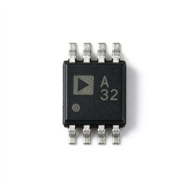
Analog Devices ADA4528-2ARMZ is a dual precision, ultralow-noise, rail-to-rail input/output (RRIO) zero-drift operational amplifier supplied in an 8-lead MSOP package. It operates from 2.2 V to 5.5 V, provides 3.4 MHz bandwidth and 0.5 V/µs slew rate, and is specified over the -40°C to +125°C industrial temperature range. The device uses a chopper-stabilized auto-zero architecture, achieving microvolt-level offset with near-zero drift over temperature and time. What is a zero-drift op amp? A zero-drift amplifier is a precision operational amplifier that continuously corrects its input offset voltage and offset drift using auto-zero or chopping techniques. Within the op amp hierarchy (operational amplifier -> precision amplifier -> zero-drift amplifier), these devices combine the low offset of a chopper with usable wideband performance. They are used where small DC signals must be amplified without adding drift or low-frequency noise. Key features include ultralow input voltage noise density of 5.6 nV/√Hz, maximum input offset voltage of 2.5 µV (family specification), excellent CMRR and PSRR, rail-to-rail input and output swing, and true zero-drift operation. The dual-channel ADA4528-2ARMZ saves board space in multi-channel precision chains and the MSOP-8 package fits compact sensor modules. The internal architecture combines a high-gain main amplifier with a continuously running nulling amplifier that corrects offset errors in the background. This provides 3.4 MHz gain-bandwidth product together with the low-frequency precision of a chopper. The result is an amplifier that can amplify microvolt-scale bridge outputs without auto-zero settling transients. Typical applications include position and pressure sensors, strain gages, medical instrumentation, load-cell/weigh-scale front ends, battery-powered portable instruments, and IoT sensor nodes. The 2.2 V minimum supply allows operation from single Li-ion cells or 3.3 V regulated rails, while the RRIO output maximizes ADC input full-scale range. Design consideration: add 0.1 µF and 10 µF decoupling capacitors close to the supply pins, and use a low-pass RC filter at the non-inverting input to minimize aliased noise when driving a sigma-delta ADC. Avoid placing the feedback network near high-impedance input traces to maintain the specified drift and noise performance.
ADA4528-2ARMZ-RL7 - Zero-Drift Dual Op Amp | Analog Devices
The ADA4528-2ARMZ-RL7 is a precision, ultralow noise, rail-to-rail input/output (RRIO) zero-drift operational amplifier from Analog Devices. It contains two independent op amps in an 8-lead MSOP package, operating from a single 2.2 V to 5.5 V supply or dual ±1.1 V to ±2.75 V supplies. This device is ideal for precision amplification of low-level signals in applications such as position and pressure sensors, strain gages, and medical instrumentation. Zero-drift amplifiers, also known as auto-zero or chopper amplifiers, are a class of operational amplifiers that continuously correct their input offset voltage and drift using a switching technique. This results in extremely low offset voltage (typically 2 µV) and near-zero drift over temperature, making them essential for high-precision DC measurement systems. The ADA4528-2 belongs to the precision op amp family, which is a subset of linear amplifiers used in signal conditioning chains. Key features include ultralow voltage noise density of 5.6 nV/√Hz, a gain-bandwidth product of 6.5 MHz, and a slew rate of 3.4 V/µs. The device also offers excellent CMRR and PSRR specifications, ensuring accurate amplification in noisy environments. The rail-to-rail input and output stages maximize dynamic range, particularly in low-voltage single-supply applications. The ADA4528-2 uses a proprietary auto-zero architecture that eliminates 1/f noise, providing a flat noise spectrum down to DC. This makes it superior to conventional amplifiers for DC precision applications. The device is specified over the extended industrial temperature range of -40°C to +125°C, ensuring reliable operation in harsh environments. Typical applications include precision sensor interfaces, thermocouple amplifiers, load cell signal conditioning, and battery-powered instrumentation. The low supply current of 1.5 mA per amplifier makes it suitable for portable devices. When designing with this device, ensure proper decoupling of the power supply pins with 0.1 µF ceramic capacitors placed close to the IC. The input common-mode range includes both rails, allowing direct interface with sensors without level shifting.
ADA4530-1ARMZ - Femtoampere Bias Current Op Amp | Analog Devices
The ADA4530-1ARMZ is a precision electrometer-grade operational amplifier from Analog Devices, designed for ultra-low input bias current applications. It features a maximum input bias current of 20 fA at 25°C, making it ideal for photodiode amplification, ion sensors, and other high-impedance measurement systems. The device operates from a single 4.5V to 16V supply or dual ±2.25V to ±8V supplies, and it is available in an 8-lead MSOP package (ARMZ suffix). An operational amplifier (op amp) is a high-gain voltage amplifier with differential inputs and a single-ended output. It is a fundamental building block in analog signal conditioning, used to amplify, filter, or buffer signals. The ADA4530-1 belongs to the class of electrometer amplifiers, which are specialized op amps with extremely low input bias current, enabling accurate measurement of currents in the femtoampere range. This makes it a critical component in scientific instrumentation and medical diagnostics. Key features of the ADA4530-1 include a low input bias current of 20 fA (max), a low offset voltage of 50 µV (max), and a low input voltage noise density of 12 nV/√Hz at 1 kHz. The device also offers a gain bandwidth product of 4 MHz and a slew rate of 2.2 V/µs, providing adequate speed for many precision applications. The rail-to-rail output stage allows maximum dynamic range, and the input common-mode range extends to the negative rail, facilitating single-supply operation. The ADA4530-1 uses low voltage MOS devices in its differential input stage, which provide better 1/f noise and bandwidth per unit current compared to high voltage devices. This architecture enables the ultra-low bias current while maintaining good noise performance. The device also includes an internal guard buffer that can be used to drive guard rings on the PCB, further reducing leakage currents. Typical applications include photodiode amplifiers, ion sensors, pH meters, and other high-impedance sensor interfaces. The device is also used in mass spectrometry, chromatography, and other analytical instruments where measuring tiny currents is essential. Its low bias current and low noise make it suitable for precision current-to-voltage conversion in these systems. When designing with the ADA4530-1, it is critical to implement proper guard ring layout and use high-quality insulating materials to minimize leakage currents. The PCB should be cleaned thoroughly to remove flux residues, and a guard ring driven by the internal guard buffer should surround the input pins. This ensures that the femtoampere bias current specification is achieved in practice.
ADA4530-1ARMZ-RL7 - Femtoampere Bias Current Op Amp | Analog Devices
The ADA4530-1ARMZ-RL7 is a precision operational amplifier from Analog Devices, specifically designed for applications requiring ultra-low input bias current. It features a femtoampere-level input bias current of 20 fA (typical) at 25°C, making it ideal for electrometer, photodiode, and other high-impedance sensor interfaces. The device operates from a single 4.5V to 16V supply or dual ±2.25V to ±8V supplies, and it provides rail-to-rail output swing. The amplifier is available in an 8-lead MSOP package (ARMZ suffix), which is optimized for guard ring routing to minimize leakage currents. An operational amplifier (op-amp) is a high-gain voltage amplifier with differential inputs and a single-ended output. It is a fundamental building block in analog electronics, used in signal conditioning, filtering, and instrumentation. The ADA4530-1 belongs to the class of electrometer-grade amplifiers, which are characterized by extremely low input bias current, enabling accurate measurement of currents in the picoampere range. This places it in the hierarchy: operational amplifier -> precision amplifier -> electrometer amplifier -> femtoampere input bias current amplifier. Key features of the ADA4530-1 include an input bias current of 20 fA (typical), a low offset voltage of 50 µV (maximum), and a low input voltage noise density of 12 nV/√Hz at 1 kHz. The device also offers a gain bandwidth product of 2 MHz and a slew rate of 1.4 V/µs. The rail-to-rail output stage allows maximum dynamic range in single-supply applications. The MSOP-8 package is compact and suitable for space-constrained designs. Technically, the ADA4530-1 uses low-voltage MOS devices in its differential input stage to achieve its exceptional bias current performance. This architecture provides better 1/f noise and bandwidth per unit current compared to high-voltage devices. The unique pinout of the MSOP-8 package is designed to prevent signal coupling between the sensitive input pins, power supplies, and output, while enabling easy routing of guard ring traces. This is critical for maintaining femtoampere-level accuracy in practical PCB layouts. Typical applications include photodiode amplifiers, ion sensors, pH meters, electrochemical sensors, and other high-impedance measurement systems. The device is also used in transimpedance amplifiers for low-level current detection, such as in mass spectrometry and particle detectors. Its low bias current and low noise make it suitable for precision instrumentation and medical devices. When designing with the ADA4530-1, it is essential to implement proper guard ring techniques and use high-quality insulating materials to minimize leakage currents. The PCB layout must be carefully planned to avoid contamination and moisture absorption, which can degrade the bias current performance. Additionally, the input pins should be protected from electrostatic discharge and overvoltage conditions.
ADA4610-1ARZ - Precision JFET Op Amp, Rail-to-Rail | Analog Devices
The ADA4610-1ARZ is a precision junction field effect transistor (JFET) operational amplifier from Analog Devices, offering a unique combination of low input noise voltage, low current noise, low offset voltage, low input bias current, and rail-to-rail output. Housed in an 8-lead SOIC package, this single amplifier operates over a wide supply range of ±4.5 V to ±15 V (or 9 V to 30 V single supply) and is specified over the extended industrial temperature range of -40°C to +125°C. An operational amplifier (op amp) is a high-gain voltage amplifier with differential inputs and a single-ended output, used in analog signal conditioning, filtering, and instrumentation. The JFET input stage provides very high input impedance and low bias current, making it ideal for interfacing with high-impedance sensors and precision measurement circuits. The ADA4610-1 belongs to the precision op amp family, which prioritizes low offset, low noise, and stability over speed. Key features include a low input voltage noise of 7.3 nV/√Hz at 1 kHz, a low input bias current of 2 pA typical, and a low offset voltage of 75 µV maximum. The rail-to-rail output stage allows maximum dynamic range in low-supply applications. The device also features a high open-loop gain of 120 dB and a unity-gain bandwidth of 16.3 MHz, balancing precision with adequate speed for many applications. Technically, the ADA4610-1 uses a precision JFET input stage combined with a rail-to-rail output stage, achieving a high slew rate of 61 V/µs. The input common-mode range extends to the negative rail, and the output swings within 20 mV of the rails. The device is fully specified at 5 V, ±5 V, and ±15 V supplies, ensuring predictable performance across common supply rails. Typical applications include precision instrumentation, active filters, data acquisition front-ends, and photodiode amplification. Its low noise and bias current make it suitable for high-impedance sensor interfaces, while the rail-to-rail output maximizes ADC input range. The ADA4610-1 is also used in medical instrumentation and industrial process control. When designing with this device, pay attention to input bias current compensation and layout to minimize leakage currents. The JFET input allows high source impedances, but PCB cleanliness is critical to avoid leakage-induced offset errors. Bypass the supply pins with 0.1 µF ceramic capacitors close to the device.
ADA4610-1ARZ-RL7 - Precision JFET Op Amp | Analog Devices
The ADA4610-1ARZ-RL7 is a precision JFET operational amplifier from Analog Devices, offering low input noise voltage, current noise, offset voltage, and input bias current, with rail-to-rail output. It operates from a single 9V to 30V supply or dual ±4.5V to ±15V supplies, making it versatile for various precision applications. The device is available in an 8-lead SOIC package and is specified over the extended industrial temperature range of -40°C to +125°C. A JFET-input operational amplifier is a type of op amp that uses junction field-effect transistors at its input stage, providing very high input impedance and low input bias current. This makes it ideal for interfacing with high-impedance sources such as sensors, photodiodes, and precision instrumentation. The ADA4610-1 belongs to the family of precision amplifiers, which are characterized by low offset voltage, low drift, and low noise, essential for accurate signal conditioning. Key features of the ADA4610-1ARZ-RL7 include a low input voltage noise of 7.3 nV/√Hz at 1 kHz, a low input bias current of 2 pA typical, and a low offset voltage of 75 µV maximum. The rail-to-rail output stage allows maximum dynamic range, and the device can drive loads up to 600 Ω. It also features a high open-loop gain of 120 dB and a common-mode rejection ratio of 110 dB, ensuring excellent accuracy. The ADA4610-1 uses a precision JFET architecture with laser-trimmed input offset voltage, achieving low drift over temperature. The device includes internal protection circuitry that allows input voltages up to 0.3 V beyond the supplies without damage. Its low noise and high input impedance make it suitable for high-impedance sensor interfaces, active filters, and precision data acquisition systems. Typical applications include precision instrumentation, medical equipment, industrial process control, and audio signal conditioning. The ADA4610-1ARZ-RL7 is particularly well-suited for photodiode amplifiers, where its low input bias current minimizes error, and for active filters requiring low noise and high accuracy. When designing with this device, ensure proper power supply decoupling with 0.1 µF ceramic capacitors close to the supply pins. The rail-to-rail output can swing within 20 mV of the rails, but for best linearity, avoid operating near the output limits. The input common-mode range extends to the negative rail, but for positive rail inputs, keep within the specified range to avoid phase reversal.

ADA4610-2ARZ - Dual Low Noise JFET Op Amp | Analog Devices
The ADA4610-2ARZ is a dual precision JFET operational amplifier from Analog Devices, offering low input noise voltage, current noise, offset voltage, and input bias current, with rail-to-rail output. It operates from a dual supply range of ±4.5V to ±15V or a single supply of 9V to 30V, and is available in an 8-lead SOIC package. This device is designed for high-precision applications requiring low noise and high accuracy. An operational amplifier (op amp) is a high-gain voltage amplifier with differential inputs and a single-ended output, used in signal conditioning, filtering, and mathematical operations. The ADA4610-2 is a JFET-input op amp, which provides very high input impedance and low input bias current, making it ideal for interfacing with high-impedance sensors and precision analog circuits. It belongs to the family of precision amplifiers, which are characterized by low offset voltage, low drift, and low noise, essential for accurate signal processing. Key features of the ADA4610-2ARZ include a low input voltage noise of 7.3 nV/√Hz at 1 kHz, a low input current noise of 0.6 fA/√Hz, a maximum offset voltage of 0.2 mV, and a typical input bias current of 5 pA. The device also offers a gain bandwidth product of 16.5 MHz, a slew rate of 61 V/µs, and a rail-to-rail output stage that swings within 50 mV of the supply rails. These specifications make it suitable for high-speed, high-precision signal conditioning. Technically, the ADA4610-2 uses a JFET input stage to achieve high input impedance and low bias current, combined with a precision bipolar output stage for low offset and noise. The device includes internal ESD protection and can withstand input voltages up to 0.3V beyond the supply rails without damage. The rail-to-rail output allows maximum dynamic range in single-supply applications, and the low noise performance is critical for applications such as medical instrumentation and audio processing. Typical applications include precision data acquisition systems, medical instrumentation, audio signal processing, active filters, and sensor signal conditioning. The low noise and low bias current make it ideal for photodiode amplifiers and high-impedance sensor interfaces. The wide supply range and rail-to-rail output also enable use in battery-powered and single-supply systems. When designing with the ADA4610-2ARZ, ensure proper power supply decoupling with 0.1µF capacitors close to the supply pins. For optimal noise performance, use low-value resistors in the feedback network and keep the input traces short. The device is specified for operation from -40°C to +125°C, making it suitable for industrial environments.
ADA4610-2ARZ-RL7 - Dual JFET Precision Op Amp | Analog Devices
The ADA4610-2ARZ-RL7 is a dual precision JFET operational amplifier from Analog Devices, offering low input noise voltage, low current noise, low offset voltage, and rail-to-rail output. It operates from a dual supply range of ±4.5 V to ±15 V or a single supply of 9 V to 30 V, and is available in an 8-lead SOIC package. This device is designed for high-precision applications requiring low noise and low input bias current. An operational amplifier (op amp) is a high-gain voltage amplifier with differential inputs and a single-ended output. It is a fundamental building block in analog signal processing, used in applications such as filtering, amplification, and signal conditioning. The ADA4610-2 is a JFET-input op amp, which provides very high input impedance and low input bias current, making it ideal for interfacing with high-impedance sensors and precision instrumentation. Key features of the ADA4610-2 include a low offset voltage of 0.4 mV maximum (B grade) and 1 mV maximum (A grade), low offset voltage drift of 4 µV/°C (B grade) and 8 µV/°C (A grade), and low input bias current. The device also features rail-to-rail output swing, which maximizes dynamic range in low-voltage applications. The input voltage noise is 7.3 nV/√Hz at 1 kHz, and the current noise is 0.8 fA/√Hz, making it suitable for low-noise signal chains. The ADA4610-2 uses a precision JFET input stage combined with a bipolar output stage, achieving a gain bandwidth product of 16.3 MHz and a slew rate of 61 V/µs. The device operates over the industrial temperature range of -40°C to +125°C and is available in an 8-lead SOIC package. The rail-to-rail output stage allows the output to swing within 50 mV of the supply rails, maximizing headroom in low-voltage designs. Typical applications include precision instrumentation, active filters, data acquisition systems, and audio signal processing. The low noise and low input bias current make it ideal for photodiode amplifiers, transimpedance amplifiers, and high-impedance sensor interfaces. The rail-to-rail output is particularly useful in single-supply systems where output swing is critical. When designing with the ADA4610-2, ensure proper power supply decoupling with 0.1 µF ceramic capacitors placed close to the supply pins. The input common-mode voltage range extends to the negative rail, but for best performance, keep the inputs within the specified common-mode range. The device is protected against input voltages up to 0.3 V beyond the supplies, but external protection may be needed for harsh environments.
ADA4610-4ARUZ - Quad Precision JFET Op Amp | Analog Devices
The ADA4610-4ARUZ is a quad-channel, precision JFET operational amplifier from Analog Devices, featuring low input noise voltage, low current noise, low offset voltage, low input bias current, and rail-to-rail output. It is available in a 14-lead TSSOP package (RU suffix) and operates over the extended industrial temperature range of -40°C to +125°C. The device is designed for high-impedance sensor amplification, precision current sensing, and other applications requiring low leakage and high accuracy. What is a JFET-input operational amplifier? An operational amplifier (op amp) is a high-gain voltage amplifier with differential inputs and a single-ended output, used in signal conditioning, filtering, and instrumentation. A JFET-input op amp uses junction field-effect transistors at its input stage, providing very high input impedance (typically >10^12 ohms) and extremely low input bias current, making it ideal for interfacing with high-impedance sources such as photodiodes, pH sensors, and piezoelectric sensors. The ADA4610-4 belongs to the precision op amp category, which emphasizes low offset voltage, low drift, and low noise for accurate signal processing. Key features of the ADA4610-4ARUZ include a low input voltage noise density of 7.3 nV/√Hz at 1 kHz, a low input current noise of 0.8 fA/√Hz, a maximum input offset voltage of 400 µV, and a typical input bias current of 1 pA. The rail-to-rail output stage allows the output to swing within 50 mV of the supply rails, maximizing dynamic range in low-voltage applications. The amplifier operates from a dual supply range of ±4.5 V to ±15 V or a single supply of 9 V to 30 V, providing flexibility in various power configurations. Technically, the ADA4610-4 uses a precision JFET architecture with internal protective circuitry that allows input voltages up to 0.3 V beyond the supply rails without damage. The device features a gain bandwidth product of 16.3 MHz and a slew rate of 61 V/µs, enabling it to handle fast signals while maintaining precision. The low input bias current is maintained even at elevated temperatures due to minimized die temperature, making it suitable for applications without active cooling. Typical applications include precision data acquisition systems, medical instrumentation, photodiode amplification, and active filters. The quad configuration in a compact TSSOP package saves board space and simplifies multi-channel designs. For example, in a multi-channel data acquisition system, the ADA4610-4 can buffer four sensor signals with minimal error. When designing with this device, ensure proper power supply decoupling with 0.1 µF ceramic capacitors close to the supply pins. The high input impedance makes the device sensitive to PCB leakage currents, so a guard ring around the input pins is recommended to maintain low bias current performance.
ADA4610-4ARUZ-RL7 - Quad JFET Op Amp, Low Noise | Analog Devices
The ADA4610-4ARUZ-RL7 is a precision quad JFET operational amplifier from Analog Devices, offering low input noise voltage, low current noise, low offset voltage, and low input bias current with rail-to-rail output. It operates over a wide supply range of ±5 V to ±15 V (or 10 V to 30 V single supply) and is specified over the extended industrial temperature range of -40°C to +125°C. The device is available in a 14-lead TSSOP package, making it suitable for space-constrained applications. A JFET-input operational amplifier is a type of op amp that uses junction field-effect transistors at its input stage, providing very high input impedance and low input bias current. This makes it ideal for applications requiring minimal loading of the signal source, such as sensor interfaces, photodiode amplifiers, and precision instrumentation. The ADA4610-4 belongs to the family of precision amplifiers, which are characterized by low offset voltage, low noise, and high DC accuracy, essential for high-resolution measurement systems. Key features of the ADA4610-4 include a low input voltage noise of 7.3 nV/√Hz at 1 kHz, a low input bias current of 2 pA (typical), and a low offset voltage of 90 µV (maximum). The rail-to-rail output stage allows maximum output swing, and the device can drive capacitive loads up to 500 pF without oscillation. The quad configuration integrates four independent amplifiers in a single package, saving board space and reducing cost per channel. The ADA4610-4 uses a precision JFET process that minimizes die temperature effects, ensuring low input bias currents even at elevated ambient temperatures. This makes it ideal for applications requiring low leakage specifications without active cooling. The internal protective circuitry allows input voltages up to 0.3 V beyond the supplies without damage, enhancing robustness in harsh environments. Typical applications include precision data acquisition systems, active filters, instrumentation amplifiers, and medical equipment. The low noise and low bias current make it particularly suited for photodiode amplification and high-impedance sensor interfaces. The rail-to-rail output enables full-scale signal swing in single-supply systems, simplifying power supply design. When designing with the ADA4610-4, ensure proper bypassing of the power supply pins with 0.1 µF ceramic capacitors placed close to the device. The input bias current is extremely low, so the use of guard rings around the input pins can help minimize leakage currents on the PCB. Also, consider the output drive capability when driving heavy loads, as the device is optimized for low power consumption.

ADA4622-1ARJZ - 30V 8MHz Low Bias JFET Op-Amp | Analog Devices
The Analog Devices ADA4622-1ARJZ is a single-channel, precision JFET-input operational amplifier housed in a 5-lead SOT-23 package (RJ-5). It operates from a single supply of 5 V to 30 V or dual supplies of ±5 V, ±15 V, and features 8 MHz gain-bandwidth product, 23 V/µs slew rate, and ultra-low input bias current of 2 pA typical. The output is rail-to-rail and the part is specified over the extended industrial temperature range of -40°C to +125°C. A precision op-amp (operational amplifier) is a high-gain DC-coupled analog building block used to amplify small differential signals while rejecting common-mode noise. JFET-input op-amps specifically use junction field-effect transistors at the input pair, which provide extremely high input impedance (typically >1 TΩ) and very low bias current, making them ideal for transimpedance amplifiers, photodiode front-ends, and high-impedance sensor signal conditioning. The ADA4622-1 belongs to the broader category of linear amplifiers -> op-amps -> precision amplifiers -> semiconductor ICs. Key differentiating features include a maximum offset voltage of just 200 µV, low offset voltage drift of 3 µV/°C, low input capacitance of 6 pF, low noise density of 11 nV/√Hz at 1 kHz, and integrated EMI filtering. The unity-gain stable topology and wide supply range allow operation from a single 5 V rail for portable instrumentation as well as ±15 V for industrial test equipment. Compared to legacy AD820-class JFET op-amps, the ADA4622-1 offers approximately 5x lower noise and 2x lower bias current. Typical applications include photodiode transimpedance amplifiers, precision current-to-voltage conversion, active filters, instrumentation front-ends, ATE (automatic test equipment) signal conditioning, and high-impedance sensor interfaces for medical and analytical instruments. The SOT-23-5 footprint makes it suitable for high-density PCB designs where PCB real estate is constrained. When designing with this part, observe the input common-mode range: at +5 V single supply the input range extends from 0 V to approximately +3 V, so for true rail-to-rail sensing above 3 V use the dual ±15 V supply configuration. Place a 100 nF decoupling capacitor directly at the supply pin, and keep input trace lengths short to minimize leakage and parasitic capacitance. This page synthesizes distributor pricing, drop-in alternative MPNs, and practical SOT-23-5 layout guidance that complements - but does not replace - the Analog Devices datasheet.
ADA4622-1ARJZ-R2 - 30V JFET Precision Op-Amp SOT-23-5 | ADI
The Analog Devices ADA4622-1ARJZ-R2 is a single-channel, 30 V, 8 MHz, low-bias-current, single-supply, rail-to-rail output (RRO) precision JFET operational amplifier in a 5-pin SOT-23 package supplied on a 7-inch reel of 250 units. It is the next-generation replacement for the legacy AD820/AD822 family, integrating JFET input stages with a precision bipolar output stage to deliver picoampere-level input bias current, low offset voltage, and rail-to-rail output swing while operating from a single 5 V to 30 V supply or dual ±5 V / ±15 V rails. According to the Analog Devices ADA4622-1/ADA4622-2/ADA4622-4 datasheet, the part is specified over the extended industrial temperature range of -40°C to +125°C and offers 8 MHz gain-bandwidth product with a typical slew rate that supports both DC precision and moderate-speed signal conditioning. A precision operational amplifier is a high-gain DC-coupled analog building block used to amplify small differential signals while rejecting common-mode noise and offset drift. JFET-input op-amps (JFET op-amp = junction field-effect transistor op-amp) extend the input impedance into the gigaohm-to-teraohm range and reduce input bias current into the picoampere range, which is essential when interfacing with high-impedance sensors, photodiodes, and transimpedance topologies. The ADA4622-1 belongs to the operational amplifier -> amplifier IC -> analog IC -> integrated circuit hierarchy, and is targeted at applications where AD820/AD822 footprints, low IB, and rail-to-rail output are simultaneously required. Key features include 8 MHz gain-bandwidth product, rail-to-rail output swing, picoampere-level input bias current, low input offset voltage, single-supply operation from 5 V to 30 V (and dual ±5 V / ±15 V), and an extended -40°C to +125°C industrial temperature range. The 5-lead SOT-23 (RJ) package is footprint-compatible with industry-standard single op-amp pinouts, easing migration from older AD820/AD822 designs. The part is specified at +5 V, ±5 V, and ±15 V supply rails, allowing a single BOM line to cover multiple system voltages. Architecturally, the ADA4622-1 combines a JFET input differential pair with a precision output stage, allowing the high-impedance input behavior of JFETs without sacrificing the output drive strength needed for rail-to-rail swing into low-impedance loads. Designers should still observe standard precision-op-amp layout practices: low-leakage PCB guard rings around high-impedance nodes, minimal stray capacitance on the inverting input, and a stable feedback network chosen to account for the 8 MHz GBW. Typical applications include photodiode transimpedance amplifiers (TIAs), precision instrumentation front-ends, high-impedance sensor signal conditioning, active filters, analog input stages for data acquisition boards, and pin-compatible upgrades of legacy AD820/AD822 designs. The combination of low IB, RRO, and wide supply range makes the part suitable for both single-supply battery-powered instrumentation and dual-supply industrial signal chains. When designing with this device, keep high-impedance traces short and consider a PTFE or low-absorption PCB material if leakage budget is critical. Input bias-current cancellation is not required for most uses, but board cleanliness (no flux residue, no moisture) is essential to preserve picoampere-level IB performance. This page synthesizes distributor pricing, verified cross-reference data from Analog Devices' SOT-23-5 footprint family, and practical PCB/layout guidance that complements (but does not duplicate) the manufacturer datasheet.
ADA4622-1ARJZ-R7 - 30V 8MHz JFET Precision Op Amp | Analog Devices
The Analog Devices ADA4622-1ARJZ-R7 is a single-channel, 30 V, 8 MHz, low-bias-current, single-supply, rail-to-rail output (RRO), precision operational amplifier supplied in a 5-lead SOT-23 (RJ) package on a 7-inch reel. It is the next-generation successor to the legacy AD820, integrating a JFET input stage with a high-voltage CMOS output stage to deliver precision DC accuracy combined with wide-bandwidth AC performance on a single supply rail as low as 5 V up to 30 V (±5 V, ±15 V typical operating points). A precision operational amplifier (op amp) is a high-gain differential voltage amplifier whose input offset voltage, input bias current, and noise are minimized so that the closed-loop behaviour of the circuit is dominated by the external feedback network rather than the device itself. Precision op amps sit at the top of the analog-IC hierarchy between general-purpose amplifiers and instrumentation amplifiers, and they form the foundational building block for signal conditioning in data-acquisition front ends, transducer bridges, photodiode transimpedance amplifiers, and active filters across industrial, instrumentation, medical, and audio systems. Key features of the ADA4622-1 include 8 MHz gain-bandwidth product, 6 pA typical input bias current (JFET input), 350 µV maximum input offset voltage (B-grade equivalent, verify on datasheet), 120 dB open-loop gain, 0.0007% THD at 1 kHz, rail-to-rail output swing, and -40 °C to +125 °C extended industrial temperature range. The part is unity-gain stable and is specified at +5 V, ±5 V, and ±15 V supply rails, simplifying mixed-voltage system design. Architecturally, the device pairs a JFET input differential pair for near-zero gate leakage with a high-voltage CMOS output stage capable of driving 2 kΩ loads to within millivolts of either rail. The combination avoids the trade-off between low bias current and high output swing that traditionally forced designers to choose either a JFET-input/bipolar-output or a CMOS-input/CMOS-output topology. Typical applications include precision current sensing with high-side or low-side shunt amplifiers, photodiode transimpedance amplifiers, active filter stages for anti-aliasing, 16-/18-bit SAR ADC drivers, instrumentation front ends, medical instrumentation signal paths, and industrial process-control analog I/O. The wide supply range also supports battery-stack monitoring and 24 V industrial-bus interfaces. When designing with the ADA4622-1 in the SOT-23-5 footprint, mind that the exposed lead frame (pin 5 / thermal tab) is internally connected to V− or to a no-connect depending on layout variant; consult the ADI datasheet before using pin 5 as a thermal pad. Decouple each supply pin with 100 nF OFL: X7R ceramic placed within 5 mm of the pin, and add a bulk 10 µF tantalum or aluminum-polymer cap to suppress load-step ringing. This page synthesizes distributor pricing, drop-in SOT-23-5 alternatives, parametric comparison, and practical design notes not found in the bare ADI datasheet, with full provenance to manufacturer documentation and cross-reference data.