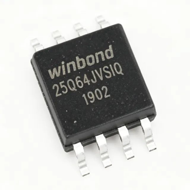
W25H02JVTBIM
W25H02JVTBIM - 2Gb QSPI NOR Flash, 24-TFBGA | Winbond
The Winbond W25H02JVTBIM is a 2 Gigabit (256M x 8) serial NOR Flash memory in a 24-pin TFBGA (8x6 mm) package, supporting standard SPI, Dual SPI, Quad SPI, QPI, and DTR (Double Transfer Rate) modes. Operating from a single 2.7V to 3.6V supply, it delivers up to 133 MHz clock rate with an equivalent throughput of 416 MHz (50 MB/s) in Quad-SPI/DTR mode. The device uses a standard SPI command set for read, program, and erase, with sector sizes of 4 KB and block sizes of 32 KB and 64 KB for flexible memory management.
Background: A NOR Flash memory is a non-volatile storage technology that retains data without power and supports random access (execute-in-place / XIP), making it ideal for code storage and boot media. The QSPI NOR category, to which the W25H family belongs, uses a 4-wire SPI interface that effectively quadruples throughput versus legacy SPI. Within the memory hierarchy, QSPI NOR sits between SRAM (volatile, fast) and NAND Flash (non-volatile, block-oriented, slower random access), serving as fast boot ROM and parameter storage in embedded systems.
Key features of the W25H02JVTBIM include uniform 4 KB sector erase, JEDEC standard manufacturer (0xEF) and device ID, hardware and software write protection, individual block and chip erase capability, and a continuous program/erase endurance of 100,000 cycles per sector. The device includes a 256-byte Security Register with OTP lockable bits for unique device identification and parameter storage, and supports single 2.7V-3.6V operation for direct connection to 3.3V MCUs.
Architecture: Built on Winbond's proprietary NOR cell technology, the W25H02JVTBIM pairs a 32-bit shift register with an integrated command controller to manage page program (up to 256 bytes per page), sector/block/chip erase, and status register polling. The DTR mode samples data on both clock edges, doubling effective throughput at the same SCK frequency. The package pinout exposes /CS, SCK, IO0-IO3, /WP, /HOLD, VCC, and GND, enabling direct connection to modern MCU QSPI controllers.
Typical applications: the W25H02JVTBIM is well suited to network router firmware storage, IoT gateway boot and data logging, set-top box / smart TV boot media, industrial HMI panel image storage, and automotive infotainment reference code where execute-in-place is required. Its 2 Gb density supports full firmware images plus room for OTA staging and asset storage.
Design consideration: For systems upgrading from legacy SPI flash, verify that the host MCU's QSPI controller supports DTR mode to realize the full 50 MB/s throughput; otherwise the part still works in single-bit SPI mode. Ensure decoupling caps are placed as close as possible to VCC and GND, and follow Winbond's recommended PCB pad pattern for the 24-ball TFBGA.
USD $2.38
재고 있음