제품 (39,000+)

EP4CE40F29I8LN - 39.6K LE Cyclone IV E FPGA, 780-FBGA | Intel
EP4CE40F29I8LN

EP4CE40F29I8LN - 39.6K LE Cyclone IV E FPGA, 780-FBGA | Intel

The Intel (formerly Altera) EP4CE40F29I8LN is a Cyclone IV E Field-Programmable Gate Array (FPGA) featuring 39,600 logic elements, 1,161,216 bits of embedded memory, and 532 maximum user I/O, packaged in a 780-ball FineLine BGA (FBGA) and fabricated on a low-power 60 nm process. It operates from a 1.2 V core supply with hot-socketing support and is rated for the industrial temperature range of -40 °C to 100 °C with speed grade 8. A Field-Programmable Gate Array (FPGA) is a semiconductor device built around an array of configurable logic blocks (CLBs), programmable interconnect, and dedicated hardware such as block RAM, DSP blocks, PLLs, and high-speed transceivers. FPGAs sit in the programmable-logic tier of the broader digital IC hierarchy between ASICs (higher NRE, higher performance) and microcontrollers (lower performance, software-driven), enabling hardware-level parallelism, deterministic latency, and field upgradability for applications where general-purpose processors cannot meet throughput or timing requirements. Key features of the EP4CE40F29I8LN include 4 input look-up tables (LUTs), 113 18x18 hardware multipliers, four general-purpose PLLs, 116 Kbits of distributed RAM, and 532 maximum user I/O pins routed through eight I/O banks supporting LVDS, LVCMOS, SSTL, and HSTL I/O standards. The device also integrates dedicated configuration logic supporting passive serial (PS), active serial (AS), and JTAG configuration modes. The Cyclone IV E architecture balances logic density, embedded memory, and DSP capability with low static and dynamic power, achieved through the 60 nm process and per-bank I/O voltage scaling. The 780-FBGA package exposes the maximum I/O count of the EP4CE40 device family, enabling high-bandwidth parallel interfaces to external memory and high-speed peripherals. Typical applications include industrial motor control and drive systems, factory automation controllers, video processing and display pipelines, telecommunications line cards, and military/aerospace avionics subsystems. The wide industrial temperature range and robust logic capacity make the EP4CE40F29I8LN well-suited to designs that require deterministic real-time performance with hardware parallelism. When designing with this device, plan I/O bank assignments carefully to avoid VCCIO bank supply conflicts, and follow the Quartus II / Quartus Prime power-up and configuration sequencing recommendations. Because the 780-FBGA package is large and BGA-routed, PCB stack-up, microvia design, and thermal management must be addressed in the early schematic/layout phase.

견적 요청 문의하기
EP4CE40F29I8N - 39.6KLE Cyclone IV E FPGA, 780-BGA | Altera
EP4CE40F29I8N

EP4CE40F29I8N - 39.6KLE Cyclone IV E FPGA, 780-BGA | Altera

The Altera (Intel) EP4CE40F29I8N is a Cyclone® IV E family FPGA housed in a 780-ball FineLine BGA (FBGA) package, delivering 39,600 logic elements, 1,161,216 bits of embedded RAM, and 532 user I/O pins in a low-power, low-cost programmable logic fabric. According to the Altera Cyclone IV E family documentation, the device integrates 4 PLLs, 116 embedded multipliers (18x18), and supports configuration via JTAG, Active Serial, and Active Parallel interfaces, making it suitable for high-volume cost-sensitive designs. A Field-Programmable Gate Array (FPGA) is a semiconductor integrated circuit that can be configured by the customer or designer after manufacturing to implement any digital logic function. FPGAs sit at the top of the programmable logic hierarchy (FPGA -> programmable logic -> digital IC -> semiconductor), offering parallel processing, high-speed I/O, and reconfigurable logic blocks that outperform fixed-function ASICs in prototyping and low-to-mid volume production. The Cyclone IV E series specifically targets cost-sensitive applications that still require FPGA performance. The EP4CE40F29I8N operates from a 1.0V to 1.2V core supply with separate 1.5V, 1.8V, 2.5V, 3.0V, and 3.3V I/O bank supplies, supporting LVTTL, LVCMOS, SSTL, HSTL, LVDS, LVPECL, and PCI/PCI-X I/O standards. It features 8 user I/O banks, 4 PLLs for clock management, 20 global clock networks, and 532 maximum user I/Os. The device supports commercial (0C to +85C), industrial (-40C to +100C), and extended industrial temperature grades, with the I8N suffix indicating industrial grade with lead-free 780-FBGA packaging. Internally, the EP4CE40F29I8N uses a TSMC 60nm low-k dielectric process, which contributes to its low static and dynamic power consumption. The logic array consists of Logic Array Blocks (LABs), each containing 16 Logic Elements (LEs) that combine a 4-input LUT, programmable register, carry chain, and register chain. Embedded memory is provided as M9K blocks (9 Kbits each) totaling 116 blocks, plus MLAB blocks for distributed RAM. The 116 18x18 multipliers enable DSP functions including FIR filters and FFT butterflies without consuming logic resources. Typical applications for the EP4CE40F29I8N include industrial motor control, video processing bridges, communication protocol bridges (UART, SPI, I2C to Ethernet or PCIe), test and measurement instrumentation, and LED video wall controllers. Its combination of 532 I/Os, embedded multipliers, and high-density logic makes it well-suited for parallel data acquisition systems and custom interface bridging in industrial automation. When designing with this FPGA, ensure proper decoupling: 1uF and 0.1uF capacitors should be placed adjacent to each power pin, with a 10uF bulk capacitor for each supply rail. The 780-FBGA package requires a multilayer PCB with microvia or via-in-pad technology for reliable assembly. JTAG programming via the Altera USB-Blaster or compatible programmer is recommended for development, with Active Serial configuration from a serial flash for production. This page synthesizes distributor pricing, same-package Cyclone IV E drop-in alternatives, and practical design considerations not consolidated on any single manufacturer or distributor page.

견적 요청 문의하기
EP4CE40U19A7N - Cyclone IV E FPGA 39.6K LE | Intel | 484-FBGA
EP4CE40U19A7N

EP4CE40U19A7N - Cyclone IV E FPGA 39.6K LE | Intel | 484-FBGA

The Intel (formerly Altera) EP4CE40U19A7N is a Cyclone IV E field-programmable gate array (FPGA) delivering 39,600 logic elements, 116,1216 bits of embedded memory, and 116 multipliers in a 484-ball FineLine BGA package with 328 user I/O pins. It is the U19 package variant of the EP4CE40 family, optimized for high-I/O-count, cost-sensitive applications. Built on a low-power 60 nm process, it balances density, performance, and power efficiency for high-volume designs. A Cyclone IV E FPGA is a reprogrammable logic device belonging to the FPGA > programmable logic > semiconductor device family. Cyclone IV E devices target low-cost, high-volume applications that require moderate logic density, embedded memory blocks, embedded multipliers for DSP operations, and a flexible I/O subsystem. They are widely used as glue logic, co-processors, and I/O expanders in industrial, automotive, communications, and consumer systems. Key features include up to 39,600 logic elements (LEs), 1,161,216 bits (113 Kbytes) of embedded SRAM, four general-purpose PLLs, 116 embedded 18x18 multipliers, and 328 maximum user I/Os. The device also integrates 66 M9K memory blocks, supports external memory interfaces including DDR/DDR2 SDRAM and QDRII SRAM, and provides configuration via standard schemes such as JTAG and Active Serial. The 484-FBGA U19 package supports industrial-grade operation from -40C to 125C junction temperature. Architecturally, the EP4CE40 uses a look-up-table (LUT) based logic fabric combined with dedicated multiplier blocks and a configurable I/O ring. The embedded transceivers and PLLs support clock management and high-speed serial interfaces, while the I/O ring supports multiple single-ended and differential I/O standards including LVDS, SSTL, and HSTL. Power consumption is typically below 1.5 W in mid-utilization designs, depending on clock and toggle rates. Typical applications include industrial motor control and factory automation, video processing and display controllers, automotive driver-assistance and infotainment subsystems, software-defined radio (SDR) baseband, and telecommunication line cards. The U19 package also suits designs requiring high pin count for parallel bus aggregation or external memory expansion. A critical design consideration is power-supply sequencing - the EP4CE40 requires VCCINT, VCCIO, and VCCA_PLL rails brought up in a specific order to prevent latch-up. Decoupling must include 100 nF high-frequency caps placed within 5 mm of each power pin and bulk capacitors to support inrush current during configuration. This page synthesizes distributor pricing, drop-in alternatives in the same 484-FBGA package, and practical design notes not found in the manufacturer datasheet.

견적 요청 문의하기
EP4CE40U19I7N - 39.6K LE Cyclone IV E FPGA, 484-FBGA | Altera
EP4CE40U19I7N

EP4CE40U19I7N - 39.6K LE Cyclone IV E FPGA, 484-FBGA | Altera

The Altera (Intel) EP4CE40U19I7N is a Cyclone IV E family Field-Programmable Gate Array (FPGA) housed in a 484-ball FineLine BGA package (U19, 19x19 mm). Built on a 60 nm low-k process, the device integrates 39,600 logic elements, 1,161,216 bits of embedded SRAM (approximately 144 Kbytes), and 328 user I/Os, making it one of the densest members of the Cyclone IV E family offered in the wire-bond-friendly U19 BGA. The OPN suffix '7' indicates a 7th-order speed grade and 'I' denotes the industrial temperature range, while 'N' indicates a lead-free / RoHS-compliant package finish. A Field-Programmable Gate Array (FPGA) is a type of programmable logic IC that combines an array of configurable logic blocks, programmable interconnect, and dedicated hardware such as block RAM, DSP blocks, and PLLs. Within the broader semiconductor taxonomy, FPGAs sit alongside ASICs, microcontrollers, and DSPs as the workhorse class for parallel, high-throughput digital signal processing. Cyclone IV E specifically targets cost-sensitive, volume-driven applications where designers need ASIC-like density and DSP performance with the flexibility and faster time-to-market of an FPGA. Key features of the EP4CE40U19I7N include 4 PLLs for clock management, 116 embedded 18x18 multipliers, configurable LVDS channels, 1.0 V/1.2 V core voltage, support for LVCMOS/LVTTL I/O standards at 1.2 V/2.5 V/3.0 V/3.3 V, and an industrial-grade -40 °C to +100 °C junction operating range. The device supports up to approximately 200 MHz internal operation on common logic paths and includes dedicated hardware for DDR/DDR2/QDRII memory interfaces that are essential for video buffering and high-bandwidth data acquisition. Architecturally, the EP4CE40U19I7N uses Altera's classic LAB (Logic Array Block) structure with 16 logic elements per LAB, an interconnect hierarchy of row/column routing, and a configuration scheme based on SRAM cells (volatile, requiring an external configuration flash such as EPCS16 or EPCS64). The combination of a fast speed grade with industrial temperature range preserves timing margin while still serving cost-sensitive designs. Typical applications include industrial motor control, factory automation controllers, video surveillance and image-processing pipelines, low-cost software-defined radio baseband, medical instrumentation front-ends, and telecom line-card glue logic. The Cyclone IV E series is widely used as a bridge between MCU/CPU hosts and high-speed analog front ends, particularly where parallel LVDS or DDR memory interfaces are required. When designing with this device, plan a 4-layer PCB with continuous ground and power planes beneath the U19 BGA, follow Altera's power distribution network guidance for the 1.0 V VCCINT rail (typically a switching regulator followed by LDO post-regulation), and route all LVDS pairs with 100 Ω differential impedance and matched skew. The U19 BGA uses 1.0 mm pitch, so via-in-pad with epoxy-filled planarization is recommended for clean signal return paths. This page consolidates distributor pricing, verified drop-in alternatives in the same 484-FBGA (U19) footprint, and practical design notes that go beyond the manufacturer datasheet alone.

견적 요청 문의하기
EP4CE55F23A7N - Cyclone IV E FPGA, 55K LE, 484-FBGA | Intel
EP4CE55F23A7N

EP4CE55F23A7N - Cyclone IV E FPGA, 55K LE, 484-FBGA | Intel

The Intel (formerly Altera) EP4CE55F23A7N is a member of the Cyclone IV E family of low-cost, low-power FPGAs built on a 60 nm process, delivering 55,856 logic elements, 2,396,160 bits of embedded memory, and 324 maximum user I/O pins in a 484-ball FineLine BGA (F23) package. It is offered in the -7 speed grade and the industrial/automotive (A7, -40C to +125C junction) temperature range with a 1.2 V core supply. An FPGA (Field-Programmable Gate Array) is a semiconductor device containing an array of configurable logic blocks (CLBs), programmable interconnect, and dedicated hard IP blocks such as block RAM, DSP blocks, and PLLs that can be reconfigured by the customer after manufacture. FPGAs occupy a unique tier in the digital logic hierarchy: above fixed-function ASICs/ASSPs in flexibility, below microprocessors in sequential performance, but uniquely capable of massive parallel datapath processing and custom high-speed I/O. Within Intel's portfolio, the Cyclone IV E family sits at the low-power, low-cost end - below Cyclone V / Cyclone 10 LP, and well below Stratix / Agilex families - targeting cost-sensitive volume applications where high transceiver counts are not required. Key feature highlights of the EP4CE55F23A7N include 55,856 logic elements arranged in 2,436 logic array blocks (LABs), 154 18x18 multipliers for hardware-accelerated DSP, 4 general-purpose PLLs and 16 global clock networks, 2.4 Mbits of embedded SRAM organized as M9K blocks, and 324 maximum user I/Os supporting LVDS, LVCMOS, SSTL, and other single-ended and differential I/O standards. The device supports configuration via JTAG, Active Serial (AS), Active Parallel (AP), and Passive Serial (PS) modes from external flash or a download cable. Typical applications for the EP4CE55F23A7N span industrial motor control, video bridging and image processing, automotive driver-assistance and infotainment pre-processing (AEC-Q100 grade), low-cost ASIC prototyping, and communications line-card glue logic. Designers choose this part when they need mid-range logic capacity (around 50K LEs), generous DSP throughput, and a wide I/O count in a proven, mature, low-power node. When designing with this device, pay attention to power-rail sequencing: VCCINT (1.2 V core) must ramp before or simultaneously with VCCA (2.5 V analog PLL supply), and VCCIO banks can be powered independently. Use the Quartus II / Quartus Prime design suite (Cyclone IV E device support) for synthesis, place-and-route, and timing closure - older Quartus II 13.0sp1 / 13.1 is the last officially supported version.

견적 요청 문의하기
EP4CE55F23C6 - Cyclone IV E FPGA, 55K LE, 484-FBGA | Intel
EP4CE55F23C6

EP4CE55F23C6 - Cyclone IV E FPGA, 55K LE, 484-FBGA | Intel

The Intel (Altera) EP4CE55F23C6 is a Cyclone IV E family field-programmable gate array (FPGA) with 55,856 logic elements, 2,396,160 bits of embedded memory, and 343 Embedded Multipliers (18x18), housed in a 484-ball FineLine BGA (FBGA) package. It is built on a low-power 60 nm process and is offered in the commercial speed grade 6 variant. An FPGA (Field-Programmable Gate Array) is a programmable logic device that lets engineers implement arbitrary digital logic, DSP blocks, memory, and high-speed I/O on a single chip, far exceeding the flexibility of fixed-function ASICs for low-to-medium volume designs. FPGAs sit at the hierarchy: programmable logic -> logic device -> semiconductor IC. The Cyclone IV E family is positioned as a low-cost, low-power family targeting cost-sensitive applications such as industrial control, video processing, and communication bridges. Key features of the EP4CE55F23C6 include 55,856 logic elements arranged in 3,491 LABs, 324 maximum user I/O pins, four general-purpose PLLs for clock management, and 8 transceiver clock inputs. It supports DDR/DDR2/QDRII+ external memory interfaces through soft memory controllers, allowing flexible high-throughput memory expansion. The 484-FBGA package provides a compact footprint with a thermal resistance suitable for forced-air or natural convection thermal designs. Architecturally, the Cyclone IV E combines an SRAM-based logic fabric with dedicated DSP multipliers and embedded M9K memory blocks. The fabric supports logic synthesis via Quartus II, including logic locking, incremental compilation, and hard PCI/PCIe IP cores. This combination gives designers sufficient density and DSP performance for moderate-throughput DSP pipelines while keeping power consumption substantially lower than the higher-tier Cyclone IV GX variants. Typical applications include industrial machine vision, motor control and drive interfaces, video format conversion and bridging, protocol conversion (e.g., UART/SPI to Ethernet or PCIe), test and measurement instruments, and low-cost ASIC prototyping. The 55K LE density is well-suited for designs that outgrow a CPLD but do not justify a high-end Cyclone IV GX or Cyclone V device. When designing with the EP4CE55F23C6, ensure the PCB accommodates the 484-ball FBGA BGA land pattern with proper via-in-pad or dog-bone fanout, and follow Intel's PCB layout guidelines for BGA break-out. The device requires multiple supply rails (core, I/O, PLL analog, and auxiliary) that must be brought up in the correct sequence; failure to do so can cause latch-up. This page synthesizes verified distributor pricing, FBGA drop-in alternatives within the Cyclone IV E family, and practical design notes that go beyond the manufacturer datasheet.

견적 요청 문의하기
EP4CE55F23C6N - Cyclone IV E FPGA, 55K LEs, 484-FBGA | Intel
EP4CE55F23C6N

EP4CE55F23C6N - Cyclone IV E FPGA, 55K LEs, 484-FBGA | Intel

The Intel (formerly Altera) EP4CE55F23C6N is a Cyclone IV E family Field-Programmable Gate Array (FPGA) with 55,856 logic elements, 2,396,160 bits of embedded memory, and 324 maximum user I/O pins, housed in a 484-ball FineLine BGA package (23 mm). It integrates 156 embedded 18x18 multipliers, 4 general-purpose PLLs, and supports core voltages down to 1.2 V with industrial temperature grade 0C to 85C. A Field-Programmable Gate Array (FPGA) is a semiconductor device built around a matrix of configurable logic blocks (CLBs) connected via programmable interconnect, allowing hardware designers to implement arbitrary digital circuits after manufacturing. FPGAs sit at the top of the programmable logic hierarchy, above CPLDs and PALs, and serve as a flexible alternative to ASICs for medium-volume designs. The Cyclone IV E family is specifically optimized for low-cost, low-power applications such as industrial control, video processing, and communications infrastructure. Key features of the EP4CE55F23C6N include 55,856 logic elements (LEs), 2,396,160 RAM bits (approximately 274 kb x 9 or 300 kb x 8 of block RAM), 156 embedded multipliers for DSP operations, 4 PLLs for clock management, and 20 global clock networks. The 484-pin FBGA package supports up to 324 user I/O pins operating across multiple I/O standards including LVDS, LVTTL, LVCMOS, SSTL, and PCI/PCI-X. The part ships in the commercial speed grade 6 and is lead-free / RoHS compliant. Architecturally, the Cyclone IV E FPGA uses a 60 nm process with a 1.2 V core supply, delivering a favorable logic-per-dollar ratio versus competing families. Configuration data can be loaded through JTAG, Active Serial (AS), Passive Serial (PS), or Fast Passive Parallel (FPP) modes using a compatible EPCS or EPCQ configuration device. The internal SRAM-based configuration allows unlimited reconfigurability, while on-chip PLLs provide precise clock synthesis for memory interfaces, high-speed transceivers (when paired with external PHYs), and general logic timing. Typical applications include industrial motor control, video surveillance and image processing, automotive infotainment prototypes, software-defined radio baseband, communications line cards, and embedded DSP coprocessors. The 55K LE capacity also makes it a popular choice for ASIC prototyping and university digital logic curricula. When designing with this FPGA, ensure your PCB layout follows Intel's 484-FBGA escape routing guidelines, use multiple GND/VCC pins for power delivery, and pair the device with an EPCS16 or EPCS64 configuration memory if standalone boot is required. Quartus Prime II (or the older Quartus II) software is required for synthesis, place-and-route, and bitstream generation. This page synthesizes distributor pricing, drop-in alternatives from the same Cyclone IV E family, and practical design notes not found in the standalone manufacturer datasheet.

견적 요청 문의하기
EP4CE55F23C7 - Cyclone IV E FPGA, 55K LE, FBGA-484 | Intel / Altera
EP4CE55F23C7

EP4CE55F23C7 - Cyclone IV E FPGA, 55K LE, FBGA-484 | Intel / Altera

The Intel / Altera EP4CE55F23C7 is a Cyclone IV E family FPGA delivering 55,856 logic elements, 3,491 logic array blocks (LABs), and 2,396,160 bits of embedded memory in a 484-ball FineLine BGA (FBGA-484) package. Built on a 60nm low-power process, it operates from a 1.2V core supply with LVCMOS/LVDS/LVPECL I/O support and 324 user I/O pins. A field-programmable gate array (FPGA) is a semiconductor device containing configurable logic blocks (CLBs), programmable interconnects, and I/O cells that engineers can re-program to implement arbitrary digital circuits. FPGAs sit between fixed-function ASICs (high NRE, low unit cost at volume) and microcontrollers (fixed ISA, sequential execution), offering hardware-level parallelism and nanosecond-level latency for DSP, glue logic, and high-speed interface bridging. Cyclone IV E is Altera's (now Intel FPGA) low-cost, low-power family targeting volume production in industrial, automotive, communications, and consumer designs. Key features of the EP4CE55F23C7 include up to 472.5 MHz internal operation, 4 transceivers (none on this E variant), 156 embedded 18x18 multipliers, and 4 PLLs for clock management. The 60nm process achieves low static and dynamic power versus prior Cyclone generations, while the FBGA-484 package provides 1.0 mm ball pitch for moderate-density PCB assembly. Configuration options include JTAG, passive serial, active serial, and fast passive parallel modes. The Cyclone IV E architecture integrates embedded memory blocks (M9K) and DSP blocks alongside general-purpose logic, enabling single-chip implementation of video pipelines, motor control, industrial protocols, and custom bus bridges. Hard intellectual property such as PCI Express soft cores and DDR/DDR2 SDRAM controllers is available via Altera / Intel Quartus IP libraries, simplifying system integration versus older glue-logic designs. Typical applications include industrial motor drives and PLCs, video surveillance image processing, factory automation controllers, software-defined radio baseband, medical imaging front-ends, and LED video walls. The wide logic capacity supports multi-protocol bridging (EtherCAT, PROFINET, CAN, RS-485) combined with on-chip DSP for sensor fusion. When designing with this FPGA, plan power sequencing for the 1.2V core, 2.5V/3.3V I/O banks, and PLL analog supplies separately, and verify signal-integrity on DDR/DDR2 interfaces with matched-length routing. Quartus Prime software (Lite/Standard/Pro editions) is required for synthesis, place-and-route, and bitstream generation. This page synthesizes distributor pricing, drop-in and same-footprint Cyclone IV E alternatives, and practical design notes not collected on a single manufacturer datasheet page.

견적 요청 문의하기
EP4CE55F23C7N - Cyclone IV E FPGA 55K LE 484-FBGA | Intel
EP4CE55F23C7N

EP4CE55F23C7N - Cyclone IV E FPGA 55K LE 484-FBGA | Intel

The Intel (formerly Altera) EP4CE55F23C7N is a Cyclone IV E family field-programmable gate array (FPGA) integrating 55,856 logic elements, 3,491 configurable logic blocks (CLBs), and 2,396,160 bits of embedded memory in a 484-ball FineLine BGA package (23 x 23 mm, 1.0 mm pitch). Built on a low-power 60 nm process, it operates from a 1.2 V core supply with hot-socketing and I/O voltages down to 1.2 V, and is rated for commercial temperature (0C to +85C). A Field Programmable Gate Array (FPGA) is a semiconductor device built around an array of configurable logic blocks (CLBs) connected by programmable interconnect, allowing the hardware function to be defined after manufacture using a hardware description language (HDL). Within the broader semiconductor taxonomy, an FPGA is a programmable logic device that sits between application-specific integrated circuits (ASICs) and general-purpose processors, combining parallel hardware performance with software-like design flexibility. Key features of the EP4CE55F23C7N include 324 maximum user I/O pins, 4 PLLs, 66 embedded 18x18 multipliers, 56 global clock networks, and up to 472.5 MHz internal clock performance in the C7 speed grade. The device supports high-speed external memory interfaces including DDR2 SDRAM and QDRII+ SRAM, and offers configuration via JTAG, Active Serial (AS), or Passive Serial (PS) modes. Compared with the higher-cost Cyclone V family, Cyclone IV E remains a preferred choice for cost-sensitive, high-volume, low-power designs. The Cyclone IV E architecture combines a low-leakage process with Cyclone series architectural advances such as multiplier blocks, M9K memory blocks, and a rich set of high-speed I/O standards (LVDS, SSTL, HSTL). This balance of logic density, memory bandwidth, and DSP capability makes the EP4CE55F23C7N suitable for protocol bridging, motor control, video processing, and industrial I/O expansion. Typical applications include industrial machine vision, motor and motion control, video format conversion, software-defined radio front-ends, LED video walls, and embedded PCIe-over-GPIO bridges. Designers frequently use the EP4CE55F23C7N as a glue-logic and DSP coprocessor alongside ARM Cortex-M or Cortex-A host processors. When designing with this device, allocate at least four PCB layers for power/ground integrity and route all VCCINT/VCCIO decoupling close to each ball. Confirm Quartus II version compatibility before board bring-up. This page synthesizes distributor pricing, drop-in alternatives, and practical design notes not found in the manufacturer datasheet.

견적 요청 문의하기
EP4CE55F23C8 - Cyclone IV E FPGA, 55K LE, 484-FBGA | Intel
EP4CE55F23C8

EP4CE55F23C8 - Cyclone IV E FPGA, 55K LE, 484-FBGA | Intel

The Intel (formerly Altera) EP4CE55F23C8 is a Cyclone IV E field-programmable gate array (FPGA) with 55,856 logic elements, 2,340 Kbits of embedded M9K SRAM, 154 embedded 18x18 multipliers, and 4 PLLs, fabricated on a 60 nm low-power process and housed in a 484-ball FineLine BGA package. It integrates 324 user I/O pins, supports a 1.2 V core supply, and is built for high-volume, cost-sensitive applications that need a balance of logic density, on-chip memory, and DSP capability. An FPGA (Field-Programmable Gate Array) is a semiconductor device built from a matrix of configurable logic blocks (CLBs) connected via programmable interconnect. FPGAs sit above microcontrollers and fixed-function ASICs in the design hierarchy: unlike an MCU they execute logic in dedicated hardware rather than software, and unlike an ASIC they are re-programmable after manufacture. The Cyclone IV E family specifically targets low-power, low-cost, transceiver-free applications that still require substantial parallel processing and DSP throughput. Key features include 55,856 logic elements, 2,340 Kbits of embedded memory arranged in M9K blocks, 154 dedicated 18x18 hardware multipliers for DSP, 4 phase-locked loops (PLLs) for clock management, and 324 maximum user I/O pins. The 1.2 V core voltage and 60 nm process enable low static power consumption, while the 484-ball FineLine BGA package exposes the full I/O count plus dedicated configuration, clock, and JTAG pins. Architecturally, EP4CE55F23C8 uses SRAM-based configuration cells organized into Logic Array Blocks (LABs), with each LAB containing 16 logic elements. Embedded M9K memory blocks can be configured as RAM, ROM, shift registers, or FIFO buffers, while the 18x18 multipliers can be paired to form 36x36 signed multipliers. The four PLLs support clock multiplication, division, phase shifting, and zero-delay buffering, enabling complex multi-clock domain designs. Typical applications include industrial motor control, video processing pipelines, automotive infotainment pre-production, prototyping for ASIC designs, test and measurement equipment, and embedded DSP subsystems. The combination of low unit cost, integrated memory, and hardware multipliers makes EP4CE55F23C8 well suited for parallel processing tasks that would otherwise require a DSP or microcontroller plus external logic. When designing with this part, ensure the JTAG chain is properly terminated and that configuration is sourced from a supported mode (AS, PS, JTAG, or fast passive parallel). The 484-FBGA package requires careful PCB layout with controlled-impedance traces for high-speed differential pairs, and thermal management must account for the device's worst-case power dissipation under sustained switching activity. This page synthesizes distributor pricing, drop-in equivalents within the Cyclone IV E family, and practical design notes not found in the manufacturer datasheet.

견적 요청 문의하기
EP4CE55F23C8L - Cyclone IV E FPGA, 55K LEs, 484-FBGA | Intel
EP4CE55F23C8L

EP4CE55F23C8L - Cyclone IV E FPGA, 55K LEs, 484-FBGA | Intel

The Intel EP4CE55F23C8L is a Cyclone IV E field-programmable gate array (FPGA) built on a low-power 60 nm process, integrating 55,856 logic elements, 2,396,160 bits of embedded memory, and 324 general-purpose I/Os into a 484-ball fine-pitch BGA (FBGA) package with 1.2 V core operation. The "L" suffix designates an industrial-grade temperature range, while the "C8" speed grade places it in the mid-speed tier of the Cyclone IV E family, balancing logic throughput against static and dynamic power consumption. A field-programmable gate array (FPGA) is a class of programmable logic device that lets designers implement arbitrary digital logic through a sea of configurable logic blocks (CLBs), routing switches, and dedicated hard IP such as multipliers and memory blocks. Within the broader taxonomy, FPGAs sit between application-specific integrated circuits (ASICs) (fixed function, high NRE) and microcontrollers (software-defined, lower throughput). The Cyclone IV E family specifically targets cost-sensitive, high-volume, low-power applications that need moderate logic density and on-chip memory. Key features of the EP4CE55F23C8L include 55,856 logic elements, 2,396,160 bits (approximately 2,340 Kb) of embedded SRAM, 156 hardware 18x18 multipliers for DSP functions, up to 4 PLLs for clock management, and support for external memory interfaces including DDR/DDR2 SDRAM and QDRII+ SRAM. The 484-FBGA package exposes 324 user I/Os, providing ample connectivity for parallel buses, LVDS links, and memory interfaces while keeping board area reasonable for industrial designs. Architecturally, the device uses Altera/Intel's classic 4-input look-up table (LUT-4) logic fabric paired with M9K memory blocks and 18x18 multiplier blocks, all stitched together by a hierarchical routing architecture. Configuration is loaded from a serial or parallel flash device through the standard passive-serial, active-serial, or JTAG paths, and Cyclone IV E devices support both volatile and non-volatile configuration schemes. The 60 nm process and 1.2 V core voltage translate into low static power relative to the prior Cyclone III generation. Typical applications include industrial motor control and machine vision, video processing and broadcast equipment, automotive infotainment prototypes, communications line cards, and embedded control systems. The 55K-LE density is well matched to mid-complexity designs such as multi-channel data acquisition, custom protocol bridging, and image processing pipelines. Because it supports Nios II soft-core processors, the device can also host Linux or bare-metal firmware for system-on-chip designs. When designing with this part, pay close attention to power sequencing on VCCINT (1.2 V) and VCCA (2.5 V) rails: VCCA must not lag VCCINT by more than a few milliseconds, and all I/O banks must be powered before signals are applied. Proper decoupling, a clean reference clock routed with controlled impedance, and adherence to the Quartus II pin connection guidelines are essential for first-pass board bring-up. This page synthesizes distributor pricing, drop-in pin-compatible variants, and practical design considerations not found in the standalone datasheet.

견적 요청 문의하기
EP4CE55F23C8LN - Cyclone IV E FPGA 55K LE 484-FBGA | Intel
EP4CE55F23C8LN

EP4CE55F23C8LN - Cyclone IV E FPGA 55K LE 484-FBGA | Intel

The Intel (formerly Altera) EP4CE55F23C8LN is a member of the Cyclone IV E family of low-power, low-cost FPGAs fabricated on a 60 nm process. It delivers 55,856 logic elements, 2,396,160 bits of embedded memory, and 324 maximum user I/Os in a 484-pin FineLine BGA (FBGA-484) package at 23 x 23 mm with 1.0 mm ball pitch. A Field Programmable Gate Array (FPGA) is a semiconductor device built around an array of configurable logic blocks (CLBs), programmable interconnects, and dedicated hard IP such as multipliers, memory blocks, and transceivers. FPGAs sit within the broader category of programmable logic devices (PLDs), which in turn belong to the digital logic integrated circuit family. Unlike fixed-function ASICs, FPGAs are reconfigured at design time to implement arbitrary digital signal processing, glue logic, control state machines, or even soft-processor subsystems. Key features of the EP4CE55F23C8LN include 156 embedded 18x18 multipliers supporting DSP-intensive designs, 4 PLLs for flexible clock synthesis, and 20 global clock networks. The device operates from a 1.2 V core supply with separate VCCPD and VCCIO banks for mixed-voltage I/O standards such as LVDS, SSTL, and LVCMOS up to 3.3 V. Its hard memory controller and PCIe interface (when available in the family) accelerate common system functions. The "N" suffix confirms lead-free / Pb-free termination consistent with RoHS. Architecturally, Cyclone IV E uses an SRAM-based look-up table (LUT) fabric with 4-input LUTs feeding adjacent registers, and dedicated carry chains for arithmetic. Logic elements are grouped into Logic Array Blocks (LABs); the EP4CE55F23C8LN contains 3,491 LABs. The 484-FBGA package exposes the maximum user-I/O count of the family for this die, ideal for high-pin-count designs. Typical applications include industrial motor control, video processing and display bridging, factory automation controllers, low-cost software-defined radio front-ends, test and measurement instrumentation, and protocol bridging between legacy and modern interfaces (UART/SPI/I2C to Ethernet/PCIe). The combination of DSP blocks and PLLs also suits motor drive encoder interpolation and multi-axis servo control loops. Design consideration: the FBGA-484 package requires careful PCB layout with microvia stack-ups and controlled-impedance traces; ensure reference schematics from the Cyclone IV E handbook are followed for decoupling and bank-power sequencing. This page synthesizes distributor pricing, drop-in Cyclone IV E variants, and practical design notes not found on any single manufacturer or distributor product page.

견적 요청 문의하기
EP4CE55F23C8N - Cyclone IV E 55K LE FPGA, 484-FBGA | Intel
EP4CE55F23C8N

EP4CE55F23C8N - Cyclone IV E 55K LE FPGA, 484-FBGA | Intel

The Intel (Altera) EP4CE55F23C8N is a Cyclone IV E field-programmable gate array (FPGA) with 55,856 logic elements, 2,340 Kbits of embedded memory, and 156 multipliers, housed in a 484-ball FineLine BGA (FBGA) package. Built on a low-power 60 nm process, it integrates 324 maximum user I/O pins and supports core voltages of 1.2 V with commercial-grade 0 to 85 C junction temperature operation. The F23 package designation indicates the 484-ball 1.0 mm pitch FineLine BGA, while C8 denotes the commercial speed grade 8 and N a lead-free (Pb-free) finish. A Field-Programmable Gate Array (FPGA) is a semiconductor device built around a matrix of configurable logic blocks (CLBs), embedded memory blocks, multipliers, and programmable I/O cells interconnected by a programmable routing fabric. FPGAs belong to the broader class of programmable logic devices (PLDs) and occupy the high-performance tier above CPLDs, enabling hardware-level parallelism for digital signal processing, custom interfaces, and glue-logic consolidation. Cyclone IV E is a low-power, cost-optimized family within Intel's Cyclone IV portfolio, positioned for high-volume, cost-sensitive applications. Key differentiating features include the dedicated 18x18 multipliers supporting DSP applications at up to 200 MHz, embedded memory blocks (M9K) totaling 2,340 Kbits for FIFO and buffer designs, up to four general-purpose PLLs per device for clock synthesis, and support for external memory interfaces including DDR/DDR2 SDRAM and QDRII SRAM. The 324 user I/O pins support LVDS, SSTL, and LVCMOS I/O standards for direct interface to modern memory and high-speed peripherals. The Cyclone IV E architecture combines the 60 nm process with a low-leakage SRAM cell to deliver low static and dynamic power consumption, typically 30 percent lower than the prior Cyclone III generation. This makes the EP4CE55F23C8N well suited for thermally constrained or fanless industrial enclosures where the 31x31 mm FBGA package offers efficient board area utilization with full signal-integrity performance. Typical applications span industrial motor control and factory automation (PLL-driven encoder feedback), video processing and image-pipeline preprocessing, communication protocol bridging (PCI Express endpoint, Ethernet MAC, UART/SPI bridges), test and measurement instrumentation (custom trigger logic, high-speed data acquisition), and display controllers for industrial HMI panels. The 55K LE capacity also supports DSP co-processing for audio codecs and software-defined radio front-ends. When designing with this device, plan FPGA I/O bank voltage assignment carefully; the EP4CE55F23C8N supports up to eight I/O banks each requiring independent VCCIO rails. For DDR2 interfaces, observe the 1.8 V VCCIO constraint and place decoupling capacitors per the Cyclone IV Device Handbook recommendations. Quartus Prime design software is the primary development toolchain. This page synthesizes distributor pricing, drop-in alternatives, and practical design notes not found in the manufacturer datasheet, giving engineers a one-stop reference for the EP4CE55F23C8N in 484-FBGA.

견적 요청 문의하기
EP4CE55F23C8N - Cyclone IV E FPGA, 55K LEs, 484-BGA | Intel
EP4CE55F23C8N

EP4CE55F23C8N - Cyclone IV E FPGA, 55K LEs, 484-BGA | Intel

The Intel (formerly Altera) Cyclone IV EP4CE55F23C8N is a low-cost, low-power FPGA built on a 60 nm process, integrating 55,856 logic elements (LEs) and 2,396,160 bits of embedded memory into a 484-ball FineLine BGA package. The device operates from a 1.2 V core supply and offers enhanced 8B/10B-capable transceivers up to 3.125 Gbps in some Cyclone IV GX variants; the EP4CE55F23C8N is the non-transceiver Cyclone IV E member with 343 user I/O and 4 PLLs. Speed grade C8 indicates a commercial temperature range (0 °C to 85 °C) and the F23 package is a 484-pin FineLine BGA (23 mm × 23 mm body, 1.0 mm pitch). A Field Programmable Gate Array (FPGA) is a semiconductor device built around an array of configurable logic blocks (CLBs) connected via programmable interconnect, allowing designers to implement arbitrary digital logic, signal-processing pipelines, and soft processor cores after PCB fabrication. FPGAs sit in the broader category of programmable logic devices (PLDs), between fixed-function ASICs and software-defined microcontrollers; their value lies in rapid prototyping, low NRE cost, and parallel hardware acceleration. Key features of the EP4CE55F23C8N include 55,856 LEs, 2,396,160 bits of RAM (312 Kbytes M9K blocks), 156 embedded 18 × 18 multipliers, four general-purpose PLLs, 343 maximum user I/O pins, and support for external memory interfaces including DDR/DDR2/DDR3, QDR II, and RLDRAM II. The device also offers 1.2 V LVCMOS/LVTTL/LVDS I/O standards with on-chip termination (OCT). Architecturally, the Cyclone IV E family delivers up to 50% lower static power than the previous Cyclone III generation through a low-k dielectric process and selectable logic-array speed versus power trade-offs, while maintaining the same Quartus II design-flow compatibility. The ALM (Adaptive Logic Module) at 8 inputs allows efficient mapping of arithmetic, multiplexer, and register-rich designs, and the variable-precision DSP blocks accelerate finite-impulse-response (FIR) and FFT kernels. Typical applications for the EP4CE55F23C8N include industrial motor-control and machine-vision front-ends, video-bridge and display controllers (HDMI/VGA/LVDS bridging), communications line cards using soft SERDES and protocol bridging, and educational/hobbyist designs where cost, low static power, and Quartus tool maturity matter more than transceiver count. Designers should note that the EP4CE55F23C8N requires 1.2 V core, 2.5 V analog PLL, and bank-specific I/O supplies; the 1.0 mm-pitch BGA demands 4- or 6-layer PCBs with microvia-in-pad stackups for escape routing. Decoupling must follow the Quartus II power-supply decoupling guidelines with 0.1 µF, 0.01 µF, and bulk capacitors distributed across each supply rail. This page synthesizes distributor pricing tiers, drop-in FPGA alternatives from the same Cyclone IV E family, and practical Quartus design-flow guidance not consolidated in the manufacturer datasheet. The EP4CE55F23C8N remains an active, in-production low-power FPGA for cost-sensitive industrial, video, and embedded designs.

견적 요청 문의하기
EP4CE55F23C9L - Cyclone IV E FPGA, 55K LE, 484-FBGA | Intel
EP4CE55F23C9L

EP4CE55F23C9L - Cyclone IV E FPGA, 55K LE, 484-FBGA | Intel

The Intel (formerly Altera) EP4CE55F23C9L is a low-power, low-cost Cyclone IV E FPGA delivering 55,856 logic elements, 2,396,160 bits of embedded memory, and 324 user I/Os in a 484-ball FineLine BGA (FBGA) package with -40C to +85C industrial temperature grade. The 'C9' speed grade is the fastest Cyclone IV E commercial/industrial grade, while the 'L' suffix denotes the lower-leakage variant. A Field Programmable Gate Array (FPGA) is a programmable semiconductor whose logic fabric, routing, and I/O cells can be configured by the customer after manufacture. FPGAs sit at the top of the digital-logic hierarchy between standard microcontrollers (fixed-function, software-driven) and application-specific integrated circuits (ASICs, fixed-function, hardware-only). Cyclone IV E FPGAs in particular are SRAM-based devices that must be configured from an external flash on every power-up, which makes them ideal for design iteration, prototyping, and low-to-medium-volume production runs. Key features include 55,856 logic elements, 156 embedded 18x18 multipliers (for DSP), 4 PLLs, 2.5 Mb of embedded SRAM, and 324 general-purpose I/Os that support LVDS, SSTL, LVCMOS, and PCI/PCI-X interfaces. The device supports up to 200 MHz of system performance and integrates a hard memory controller for DDR/DDR2/DDR3 SDRAM, QDR II SRAM, and RLDRAM II. Hard PCIe hard IP blocks are not present on Cyclone IV E (those are Cyclone IV GX), but soft PCIe cores can be implemented in the fabric. Typical applications include industrial motor control, video processing pipelines, telecom bridging, low-cost ASIC prototyping, and embedded vision. The combination of embedded multipliers, large memory, and abundant I/O makes EP4CE55F23C9L a strong fit for parallel DSP workloads such as FIR filtering, FFT engines, and image preprocessing where a microcontroller's sequential execution model becomes a bottleneck. Design consideration: the 'L' (low-leakage) variant reduces static current versus the standard core but at the cost of slightly slower timing closure. Ensure your Quartus Prime timing analysis reflects the chosen speed grade, and budget sufficient decoupling capacitance near the BGA power balls to meet the device's dynamic current demand. This page synthesizes distributor pricing from Mouser/DigiKey/Heisener, lists drop-in same-package variants from the Cyclone IV E family, and provides drop-in decision guidance not found in the manufacturer datasheet alone.

견적 요청 문의하기
EP4CE55F23C9LN - Cyclone IV E FPGA 55K LE | Altera
EP4CE55F23C9LN

EP4CE55F23C9LN - Cyclone IV E FPGA 55K LE | Altera

The Altera EP4CE55F23C9LN is a Cyclone IV E field-programmable gate array (FPGA) with 55,856 logic elements, 2,396,160 RAM bits, and 324 user I/O, supplied in a 484-ball FBGA (F23) package. The device runs from a 1.2 V core, is built on a 60 nm process, and uses a lead-free (N) terminal finish according to Intel/Altera ordering data. A field-programmable gate array (FPGA) is a semiconductor device containing reprogrammable logic fabric and programmable routing. Designers configure the logic elements with HDL to implement parallel custom hardware rather than a fixed instruction-set processor. In the broader taxonomy, an FPGA belongs to programmable logic -> FPGA/CPLD -> integrated circuit, and Cyclone IV is a low-cost, low-power FPGA family optimized for high-volume applications. Key features include 55,856 logic elements, organized as 3,491 LAB/CLB blocks; 2,396,160 embedded RAM bits; and 324 general-purpose user I/O. The 60 nm low-power process and 1.2 V core reduce static and dynamic power versus earlier Cyclone families. The speed-grade designator and commercial temperature rating make this part a middle-cost configuration suitable for controlled-environment equipment. The EP4CE55F23 is part of the Cyclone IV E device table that shares the same 484-ball FBGA footprint across EP4CE55 package variants. The fabric uses logic array blocks, each containing sixteen logic elements, and third-party specification data lists 3,491 CLBs. It includes block RAM for data buffering, external memory interfaces, LVDS I/O support, and clock networks. The absence of hard transceivers means high-speed serial links need external PHY/transceiver devices or a different FPGA family with hardened SerDes. Typical applications include industrial motor control, software-defined radio digital front-ends, video and image processing, medical imaging front-ends, test and measurement instrumentation, and IoT edge gateways. With 324 I/O, this FPGA can connect to many ADCs, DACs, memory devices, and system buses while keeping parallel processing in hardware. When designing the 1.2 V power delivery, provide separate low-impedance rails for core and I/O and place decoupling capacitors close to the BGA balls. Because FBGA-484 uses 1 mm pitch, a four-layer PCB with via fanout under the package is recommended; use simulation or a reference design for pin assignments. Ensure configuration device and clock termination are planned before layout. This page synthesizes verified distributor inventory, pricing as of 2026-09-10, package-compatible Cyclone IV alternatives, and design guidance not found in typical distributor listings.

견적 요청 문의하기
EP4CE55F23I7 - 55,856-Cell FPGA | Intel | Industrial Control
EP4CE55F23I7

EP4CE55F23I7 - 55,856-Cell FPGA | Intel | Industrial Control

Intel EP4CE55F23I7 is a Cyclone IV E field-programmable gate array with 55,856 logic cells, 324 programmable I/O pins, and a 472.5 MHz stated frequency, housed in a 484-ball BGA package measuring 23 mm by 23 mm. The verified source data identifies the package as 484-BGA and also describes a 1 mm ball pitch. It is an FPGA IC intended for configurable digital logic, interface bridging, control processing, and high-density embedded applications. A field-programmable gate array is a semiconductor device containing programmable logic blocks, routing resources, and configurable I/O. Engineers configure the FPGA after board assembly to implement digital functions without manufacturing a custom ASIC. Within the semiconductor hierarchy, an FPGA belongs to programmable logic and is used where parallel processing, fast development, field updates, or interface flexibility justify its configuration complexity. The headline density is 55,856 cells, with 3,491 configurable logic blocks and 324 I/O pins. The product listings also identify 2,396,160 embedded memory bits and a 472.5 MHz frequency. These figures place the device in a useful middle-density class for control planes, communication interfaces, test equipment, image processing, and custom accelerators. The high pin count supports multiple parallel external interfaces within one package. The part is associated with a 60 nm Cyclone IV E architecture according to the provided comparison result for another Cyclone IV E device. The I7 ordering suffix in the verified MPN denotes the identified industrial-grade ordering variant, but exact electrical limits should be confirmed from the manufacturer ordering information. The 484-BGA package is a surface-mount package family with a dense area-array interconnect and a 1 mm pitch. Typical applications include industrial automation, motor-control coordination, communication infrastructure, test and measurement, video and imaging, and embedded control. In these systems, the FPGA can consolidate deterministic control logic, timing, protocol handling, and data processing. The 324 I/O count is especially useful when the design must connect several sensors, converters, memory devices, or communications ports. Designers should allocate power, decoupling, clock distribution, configuration storage, and signal-integrity resources before routing. BGA assembly requires controlled fabrication, and every high-speed interface must be evaluated for impedance, crosstalk, and return-path continuity. Designers should also verify the exact supported transceiver, memory-interface, voltage, temperature, and speed-grade limits in the manufacturer documentation rather than infer them from family-level descriptions. This page combines the exact distributor and manufacturer values supplied for EP4CE55F23I7 with structured package mapping, practical integration guidance, and comparison data. Where the supplied sources do not establish a specification, the result is explicitly marked rather than estimated.

견적 요청 문의하기
EP4CE55F23I7N - 55K LE Cyclone IV E FPGA 484-BGA | Intel
EP4CE55F23I7N

EP4CE55F23I7N - 55K LE Cyclone IV E FPGA 484-BGA | Intel

The Intel (formerly Altera) EP4CE55F23I7N is a low-cost, low-power Cyclone IV E Field-Programmable Gate Array with 55,856 logic elements, 2,396,160 bits of embedded memory, and 324 maximum user I/O pins, packaged in a 484-ball FineLine BGA (FBGA-484) at 23x23 mm with 1.0 mm pitch. The "I7" speed/temperature grade suffix denotes the industrial temperature range and 7th-fastest speed bin per the Altera/Intel Cyclone IV ordering convention. A Field-Programmable Gate Array (FPGA) is a reconfigurable semiconductor device whose logic, memory, and I/O blocks can be programmed by the end user to implement arbitrary digital functions. FPGAs sit in the programmable-logic layer of the digital design hierarchy - above fixed-function ASICs and microcontrollers in flexibility, below them in per-unit cost at very high volumes. The Cyclone IV E family is positioned for high-volume, cost-sensitive applications such as industrial control, video processing, and communications infrastructure, balancing logic density, DSP capability, and static power. Key features of the EP4CE55F23I7N include 3,491 configurable logic blocks (CLBs) arranged as logic array blocks (LABs), 56 embedded 18x18 multipliers for moderate DSP throughput, 4 phase-locked loops (PLLs) for flexible clock management, and an industrial operating junction temperature range of -40C to +100C. The device supports a broad mix of I/O standards including LVDS, LVCMOS, SSTL, and HSTL, and offers dedicated DDR/DDR2/QDRII memory interfaces with hard PHY blocks to reduce soft-logic overhead. Architecturally, the Cyclone IV E family uses a TSMC 60 nm low-power process with 1.2 V core operation, separately powered programmable I/O banks that each support single-ended and differential standards, and an on-chip configuration controller that supports JTAG, AS, PS, and FPP configuration modes. Hard IP blocks such as memory controllers and PLLs reduce soft-logic utilization and improve timing closure, while the 324 user I/Os are partitioned across 8 I/O banks for board-level signal-routing flexibility. Typical applications include industrial machine vision, video surveillance and broadcast infrastructure, motor and motion control, automotive infotainment prototypes, wireline/wireless bridge and aggregation equipment, and medical imaging front-ends. The combination of high logic density and a generous user-I/O count makes the EP4CE55F23I7N particularly suitable for mid-range digital signal aggregation designs. When designing with this part, plan thermal dissipation carefully - the 1.0 mm pitch FBGA requires a multi-layer PCB with via-in-pad and a solid ground/power plane stack-up. Quartus II (or Quartus Prime Lite) is required for synthesis, place-and-route, and timing analysis. Configuration memory size must be sized appropriately for the chosen bitstream compression setting. This page synthesizes distributor pricing, drop-in alternatives, and practical design notes not found in the manufacturer datasheet.

견적 요청 문의하기
EP4CE55F23I8L - Cyclone IV E 55K LEs FPGA | Intel | 484-FBGA
EP4CE55F23I8L

EP4CE55F23I8L - Cyclone IV E 55K LEs FPGA | Intel | 484-FBGA

The Intel (Altera) EP4CE55F23I8L is a low-power, high-volume Cyclone IV E Field Programmable Gate Array (FPGA) IC integrating 55,856 logic elements, 2,396,160 bits of embedded memory, and 324 user I/O pins in a 484-ball FineLine BGA (FBGA) package. Built on a 60 nm process with a 1.2 V core supply, the device belongs to the Cyclone IV E family targeting cost-sensitive, high-volume applications across industrial, automotive, communications, and consumer markets. A Field Programmable Gate Array (FPGA) is a type of programmable logic device that combines the architecture of gate arrays with the configurability of software. FPGAs occupy a unique position in the semiconductor hierarchy, sitting between fixed-function Application-Specific Integrated Circuits (ASICs) and general-purpose microcontrollers. Within that hierarchy, the Cyclone IV E family is positioned as a low-cost, low-power FPGA branch of Intel's programmable logic portfolio, optimized for high logic density per dollar and per watt, and it remains a popular choice for legacy designs and long-lifecycle industrial platforms. Key features of the EP4CE55F23I8L include 55,856 logic elements, 2,396,160 bits of embedded RAM (approximately 234 KByte), 156 embedded 18x18 multipliers, four general-purpose PLLs, and 324 maximum user I/O pins. The device supports a wide range of I/O standards including LVDS, LVTTL, LVCMOS, SSTL, and HSTL. Configuration is supported via active serial (AS), passive serial (PS), and JTAG modes, with optional on-chip encryption for design security. The Cyclone IV E architecture separates logic into logic array blocks (LABs) of 16 logic elements each, with embedded memory blocks (M9K) of 9 Kbit each arranged in columns. The I/O structure consists of banks supporting independent voltage standards, and the four PLLs provide flexible clock management with multiply, divide, phase shift, and duty cycle control. The 484-FBGA package provides ample signal escape for high I/O-count designs while fitting in a 23 x 23 mm body. Typical applications include industrial motor control and factory automation, video processing and surveillance, telecommunications line cards and protocol bridging, automotive infotainment and driver assistance subsystems, and test and measurement instrumentation. The combination of mid-range logic capacity, generous embedded memory, and wide I/O count also suits programmable I/O expansion and legacy ASIC prototyping. When designing with this device, pay close attention to bank voltage assignments and reference voltage pins - mismatched VREF can permanently damage I/O banks. The Quartus II / Quartus Prime design suite from Intel is required for synthesis, place-and-route, and bitstream generation; timing closure is typically the most challenging aspect for designs exceeding 70% logic utilization. Industrial temperature grade parts are ideal for harsh environment designs. This page synthesizes distributor pricing, same-family drop-in alternatives, and practical Quartus design notes not always present in the manufacturer's datasheet, offering engineers a one-stop decision reference for sourcing and selection.

견적 요청 문의하기
EP4CE55F23I8LN - 55K FPGA, 484-BGA | Altera | Embedded Logic
EP4CE55F23I8LN

EP4CE55F23I8LN - 55K FPGA, 484-BGA | Altera | Embedded Logic

Altera EP4CE55F23I8LN is a Cyclone IV E field-programmable gate array with 55,856 logic elements, 2,396,160 bits of embedded memory, and 324 maximum user I/O pins. The device is fabricated using a 60 nm process and is supplied in a 484-ball plastic/epoxy BGA package identified as F23/484-BGA. The verified ordering-code details identify an industrial temperature-grade device, while exact supported I/O standards, logic-element count nomenclature, and configuration features should be confirmed in the current manufacturer ordering information. A field-programmable gate array is a semiconductor device containing programmable logic blocks, programmable interconnects, and configurable I/O cells. Unlike a fixed-function application-specific integrated circuit, an FPGA can be configured after manufacturing to implement combinational logic, sequential state machines, interfaces, digital signal processing, and bus controllers. Within the semiconductor hierarchy, it belongs to programmable logic, then digital logic, then integrated circuits. Cyclone IV E devices are positioned as low-cost, low-power FPGAs for high-volume and cost-sensitive systems. The headline capacity of EP4CE55F23I8LN includes 55,856 logic elements, 2,396,160 bits of embedded memory, and 324 maximum user I/O pins. The 60 nm process and 1.2 V supply value are reported in the supplied specification data. The 484-BGA package provides a high-density surface-mount interface for complex designs, but its fine-pitch ball array requires controlled PCB fabrication, assembly, inspection, and power-delivery design. The MPN suffix I8 indicates the industrial ordering variant, although complete electrical and environmental limits are not included in the provided snippets. Cyclone IV E architecture is suitable for designs requiring flexible logic, embedded memory blocks, configurable I/O, and hardware parallelism. The device can implement custom bridges, control logic, test fixtures, and low-to-moderate throughput signal processing without requiring a mask revision. The supplied data does not expose operating frequency, transceiver count, block RAM organization, phase-locked-loop count, or exact I/O bank assignments; those values are marked as needed elsewhere rather than inferred from the family name. Typical applications include industrial control and automation, communications infrastructure, video or image-interface bridging, test and measurement equipment, and custom embedded controllers. Its 55,856 logic elements provide capacity for parallel datapaths and multiple peripheral controllers, while 324 maximum user I/O pins support wide external interfaces. Designers must partition logic carefully, verify memory and timing resources, and confirm that the selected package, ball map, configuration interface, and I/O voltage requirements match the PCB. A primary design trade-off is density versus verification effort. Increasing FPGA utilization can improve integration, but reduces timing margin, routing freedom, power headroom, and design headroom. Review the manufacturer documentation, Intel/Altera device-support resources, configuration schematic, and PCB escape routing before release to fabrication. The exact package drawing and full pinout should be taken from the manufacturer data because the provided web data confirms 484 balls but does not provide a reliable per-ball table. This page combines verified MPN capacity, package, process, memory, I/O, stock, and datasheet information with application guidance, selection constraints, and a drop-in-alternative review. It distinguishes the 484-BGA EP4CE55F23I8LN from parts with different packages, densities, temperature grades, or speed grades that cannot safely be treated as direct replacements.

견적 요청 문의하기
EP4CE55F29C6 - Cyclone IV E FPGA, 55K LEs, 780-BGA | Intel
EP4CE55F29C6

EP4CE55F29C6 - Cyclone IV E FPGA, 55K LEs, 780-BGA | Intel

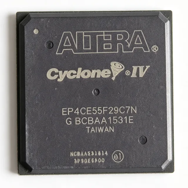
The Intel (formerly Altera) EP4CE55F29C6 is a member of the Cyclone IV E family of low-cost, low-power FPGAs fabricated on a 60 nm process. It integrates 55,856 logic elements, 239,6160 bits of embedded memory (234 Kb), and 374 user I/O pins into a 780-ball FineLine BGA package. Core logic operates from a 1.2 V supply with PLL and I/O banks fed from separate rails, supporting commercial temperature grade operation. A Field-Programmable Gate Array (FPGA) is a semiconductor device containing configurable logic blocks (CLBs), routing interconnects, and I/O cells that designers program after manufacture to implement custom digital circuits. FPGAs occupy a unique position in the silicon hierarchy - more flexible than an ASIC or microcontroller, more deterministic than a software-defined CPU. The Cyclone IV E family sits between low-density CPLDs and high-end Stratix FPGAs, targeting cost-sensitive applications such as industrial control, video bridging, motor control, and I/O expansion. Key features of the EP4CE55F29C6 include 4 phase-locked loops (PLLs) for clock synthesis, 156 embedded 18x18 multipliers for DSP and signal processing, support for external memory interfaces including DDR/DDR2 SDRAM and QDR II SRAM, and dedicated LVDS pairs on every I/O bank. Configuration is supported through JTAG, Active Serial (AS), Active Parallel (AP), and Passive Serial (PS) modes, with optional AES-128 bitstream encryption on security-sensitive builds. The Cyclone IV E architecture combines an FPGA fabric with hard IP blocks such as memory controllers, multipliers, and PLLs. Compared with the previous Cyclone III generation, Cyclone IV E offers higher logic density, lower static power, and up to 150 MHz performance on internal logic with up to 200 MHz on external memory interfaces. The fabric uses 8-input adaptive logic modules (ALMs) and supports M9K memory blocks with true dual-port capability. Typical applications include industrial machine vision and factory automation controllers, motor drive and encoder interfaces, video format conversion (HDMI/VGA/DisplayPort bridging), telecommunications line cards, USB/Ethernet interface bridges, embedded soft-core processors (NIOS II / RISC-V), and educational/development platforms. The 780-ball FBGA package supports high pin counts required by parallel external memory buses, multiple LVDS channels, and GPIO-heavy designs. When designing with this device, careful attention must be paid to power sequencing, decoupling, and thermal dissipation. The 780-FBGA package has a junction-to-ambient thermal resistance in the range of typical high-density BGA packages, so sufficient PCB copper and airflow are required for high-utilization designs. Quartus II / Quartus Prime development tools are required for synthesis, place-and-route, and timing closure. This page synthesizes distributor pricing, same-family drop-in alternatives, and practical board-level design notes not consolidated on any single manufacturer or distributor page.

견적 요청 문의하기
EP4CE55F29C6N - 55K LE Cyclone IV E FPGA | Intel | 780-BGA
EP4CE55F29C6N

EP4CE55F29C6N - 55K LE Cyclone IV E FPGA | Intel | 780-BGA

The Intel (formerly Altera) EP4CE55F29C6N is a Cyclone IV E family field-programmable gate array (FPGA) featuring 55,856 logic elements, 239,6160 memory bits, and 374 18x18 multipliers, housed in a 780-ball fine-pitch BGA (FBGA-780) package with 1.0 mm pitch and 29 x 29 mm body. What is an FPGA? An FPGA (field-programmable gate array) is a reprogrammable digital IC that combines configurable logic, embedded memory blocks, and DSP slices on a single die. FPGAs sit alongside microcontrollers and ASICs in the digital IC hierarchy, and within the Intel/Altera portfolio the Cyclone IV E series targets cost-sensitive, high-volume, low-power applications with a 60 nm process and logic densities from about 6K to 114K logic elements. Cyclone IV E specifically excludes transceivers, distinguishing it from the Cyclone IV GX family. Key features of the EP4CE55F29C6N include up to 472.5 MHz maximum operating frequency, support for LVDS, LVCMOS, SSTL, and HSTL I/O standards, up to 4 PLLs, and configuration via JTAG, passive serial, or Altera EPCS configuration devices. The device supports both 1.2 V core and 2.5 V/3.3 V I/O banks, with embedded 9 Kbit memory blocks (M9K) configurable as RAM, ROM, or FIFO. Architecturally, the EP4CE55F29C6N is built on a TSMC 60 nm low-power process, with 4 input look-up tables (LUTs) per logic element, dedicated carry chains, and embedded multiplier blocks optimized for DSP workloads. The device includes 4 PLLs and 20 global clock networks, enabling complex clock-domain designs. The 780-BGA package provides ample I/O for high-pin-count applications while maintaining a moderate footprint for the logic density offered. Typical applications include industrial motor control, video processing and image pipelines, communications infrastructure (bridges and protocol converters), test and measurement instrumentation, and embedded computing where parallel processing outperforms microcontrollers. The combination of DSP blocks and embedded RAM also suits software-defined radio (SDR) front-end processing. When designing with the EP4CE55F29C6N, pay close attention to power sequencing - core voltage (1.2 V) must ramp before I/O voltages, and proper decoupling per Altera's Cyclone IV handbook is critical for signal integrity. JTAG chain ordering matters when multiple devices share a configuration bus.

견적 요청 문의하기
EP4CE55F29C7 - Cyclone IV E FPGA, 55K LE, 780-FBGA | Intel
EP4CE55F29C7

EP4CE55F29C7 - Cyclone IV E FPGA, 55K LE, 780-FBGA | Intel

The Intel (formerly Altera) Cyclone IV EP4CE55F29C7 is a low-cost, low-power field-programmable gate array (FPGA) fabricated on a 60 nm process, offering 55,856 logic elements, 2,396,160 bits of embedded memory, and 374 maximum user I/O pins in a 780-ball fine-pitch BGA (FBGA-780) package measuring 29 x 29 mm with 1 mm pitch. The device integrates 3,491 configurable logic blocks (CLBs), 156 embedded 18x18 multipliers, and 4 phase-locked loops (PLLs), supporting up to 472.5 MHz maximum operating frequency. Core logic operates at 1.2 V with multi-voltage I/O banks supporting 1.2 V to 3.3 V interfacing. A Cyclone IV E FPGA is a programmable logic device that sits in the broader hierarchy of programmable logic -> FPGA -> SRAM-based FPGA -> low-power FPGA family. Cyclone IV E targets cost-sensitive, power-conscious applications by replacing discrete logic, microcontrollers, and ASSPs with a single reprogrammable silicon platform that can implement custom parallel processing pipelines, DSP blocks, and custom peripheral bridges. The 'E' variant emphasizes logic density and DSP capability while keeping static power low for volume production. Key features include 55,856 logic elements, 2,396,160 embedded memory bits (arranged in M9K blocks), 156 embedded multipliers, 4 PLLs, and 20 global clock networks. The device supports up to 374 user I/O pins across multi-voltage I/O banks, with LVDS, LVTTL, LVCMOS, SSTL, and HSTL I/O standards supported. Peripherals include JTAG boundary-scan, configuration via serial/parallel flash, and a dedicated Active Serial (AS) configuration interface. The Cyclone IV E architecture uses a 60 nm process node and a logic-array-block (LAB) structure, with each LAB containing 16 logic elements. Embedded multiplier blocks support DSP applications including FIR filters, FFT engines, and video processing without consuming general-purpose logic. Configuration is stored in SRAM, requiring an external configuration device such as the EPCS or EPCQ series flash. Typical applications include industrial motor control, video processing and image aggregation, software-defined radio (SDR) baseband, test and measurement equipment, automotive driver assistance and infotainment subsystems, and PCI Express endpoint bridges. The combination of high logic density, DSP multipliers, and PLLs makes Cyclone IV E particularly suited to parallel data-path designs where microcontrollers cannot meet throughput requirements. When designing with the EP4CE55F29C7, ensure adequate decoupling on every power rail (VCCINT, VCCA, VCCIO banks) and follow Intel's recommended configuration scheme for the selected configuration device. The 780-FBGA package requires fine-pitch PCB layout with 1 mm ball pitch - a 4-6 layer stack-up with dedicated ground and power planes is recommended to maintain signal integrity at LVDS rates. This page synthesizes distributor pricing across nine channels, lists drop-in same-family variants, and provides PCB layout and configuration guidance not consolidated on the manufacturer datasheet front page.

견적 요청 문의하기
EP4CE55F29C7N - 55K LE Cyclone IV E FPGA, 780-FBGA | Intel
EP4CE55F29C7N

EP4CE55F29C7N - 55K LE Cyclone IV E FPGA, 780-FBGA | Intel

The Intel (formerly Altera) EP4CE55F29C7N is a Cyclone IV E family Field-Programmable Gate Array (FPGA) delivering 55,856 logic elements, 2,396,160 RAM bits, and 374 user I/Os in a 780-ball FineLine BGA (FBGA) package with 1.0 mm ball pitch. It targets cost-sensitive applications that need more logic density than Cyclone IV E entry-level devices, with 3,491 configurable logic blocks (CLBs) and embedded 18x18 multipliers suitable for DSP and signal-processing pipelines. An FPGA (Field-Programmable Gate Array) is a programmable logic device composed of an array of configurable logic blocks (CLBs), programmable interconnect, and I/O cells, all of which the designer configures after manufacture using an HDL (Hardware Description Language) such as Verilog or VHDL. FPGAs sit at the same level of the programmable-logic hierarchy as CPLDs (Complex Programmable Logic Devices) but offer vastly greater logic capacity and embedded memory, and they belong to the broader semiconductor family of programmable logic ICs. The Cyclone IV E sub-family is Intel's low-power, low-cost line of SRAM-based FPGAs optimized for volume production in industrial, consumer, and automotive markets. Key features include 2,396,160 bits of embedded SRAM organized as M9K blocks, up to 374 user I/O pins supporting multiple I/O standards (LVDS, LVTTL, LVCMOS, SSTL, HSTL), and up to 4 PLLs (Phase-Locked Loops) for clock management. The device supports Nios II embedded processor soft cores, allowing designers to integrate a 32-bit RISC microcontroller directly into the FPGA fabric. Configuration is via JTAG, Active Serial, or Passive Parallel modes, with built-in decompression and encryption engines protecting design IP. Typical applications include industrial motor control and robotics, video processing and image pipelines, automotive driver-assistance subsystems, communications infrastructure, and consumer electronics that require custom logic, DSP, or high-speed parallel interfaces. The -7 speed grade (C7) places it in the mid-performance tier of the Cyclone IV E family, balancing timing margin against cost for mainstream designs. When designing with this device, ensure PCB layout accommodates the 1.0 mm-pitch FBGA with appropriate microvia stack-up and decoupling strategy. Power estimation with the Intel Quartus Prime Early Power Estimator is strongly recommended before final pin assignment, since core and I/O supply currents vary significantly with logic utilization and toggle rates.

USD $138.00 문의하기