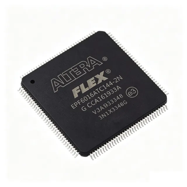
EPF6016AT1144-3N
EPF6016AT1144-3N - FLEX 6000 FPGA 16K Gates | Altera TQFP-144
The Altera (Intel) EPF6016AT1144-3N is a member of the FLEX 6000 family of SRAM-based programmable logic devices (PLDs), delivering approximately 16,000 typical gates in a 144-pin TQFP (T144) thin quad flat pack package. Built on a 0.42 µm CMOS SRAM process, the device integrates 1,320 logic elements (LEs), 16,000 typical gates, and a maximum of 132 user I/O pins operating at 3.3 V I/O with a 5.0 V tolerant input option. The "A" suffix designates the higher-performance -3 speed grade (commercial), optimized for medium-density glue logic, bus interfacing, and state-machine consolidation in cost-sensitive industrial, communications, and consumer designs.
A field-programmable gate array (FPGA) is a semiconductor integrated circuit that engineers can configure after manufacturing to implement custom digital logic functions. FPGAs sit within the programmable logic hierarchy alongside CPLDs, PALs, and GALs, but offer higher logic density, distributed register-rich architectures, and on-chip SRAM configuration memory. The FLEX 6000 family specifically targets low-to-mid density glue-logic replacement of discrete 74-series TTL and 4000-series CMOS parts, while providing non-volatile in-system reconfigurability through external configuration memory (EPC2, EPC1441).
Key features of the EPF6016AT1144-3N include 16,000 typical gates (24,000 maximum), 1,320 logic elements arranged in logic array blocks (LABs), 16,704 RAM bits distributed across embedded array blocks (EABs), and 132 user I/O pins. The device supports in-system programmability (ISP) via the ByteBlasterMV or BitBlaster download cable, multi-voltage I/O (MVIO) operation, and IEEE 1149.1 boundary-scan test (JTAG). The 144-pin TQFP package provides a robust plastic surface-mount footprint for industrial-temperature operation and automated assembly.
The FLEX 6000 architecture employs a four-input look-up table (LUT) per logic element, fast carry chains for arithmetic operations, and dedicated cascade chains for wide fan-in functions. Each LE contains a programmable register that can be configured as D, T, JK, or SR flip-flop with independent clock, clock-enable, and clear/preset controls. Embedded array blocks (EABs) deliver up to 2,048 bits of dual-port RAM per block, supporting FIFO buffers, ROM look-ups, and arithmetic coefficient storage. The continuous FastTrack interconnect routes signals across all LABs and EABs with predictable, deterministic timing.
Typical applications include industrial control and factory automation glue logic, telecommunications line-card bus interfaces, consumer electronics display controllers, networking peripheral bridges, and embedded system I/O expansion. The EPF6016AT1144-3N is also widely used in legacy PCI bus interfaces, microcontroller peripheral expansion, and as a configuration-memory controller in multi-FPGA systems. Its moderate density and low non-recurring engineering (NRE) cost make it an excellent choice for low-volume production or prototyping where ASIC conversion is not economically justified.
When designing with this device, ensure the supply rails (VCCINT 3.3 V and VCCIO 3.3 V or 2.5 V) are decoupled with 0.1 µF ceramic capacitors placed within 6 mm of every VCC pin, and that the JTAG TCK signal is properly terminated to avoid configuration errors. Designers migrating from MAX 7000 or MAX 3000 CPLDs to FLEX 6000 should be aware that FLEX 6000 is SRAM-based and loses configuration on power-down, requiring an external configuration PROM such as the EPC2 or EPC1441.
This page synthesizes FLEX 6000 family datasheet parameters, drop-in package-compatible alternatives from the same family, and practical design notes not found in distributor listings.
견적 요청
문의하기