제품 (39,000+)

MK2308S-2 - 133.3MHz Zero-Delay PLL Buffer | Renesas
MK2308S-2

MK2308S-2 - 133.3MHz Zero-Delay PLL Buffer | Renesas

The Renesas Electronics MK2308S-2 is a zero-delay PLL clock buffer operating up to 133.3 MHz, with one clock circuit and PLL bypass support in a 16-SOIC package measuring 0.154 inch, or 3.90 mm, wide. The device is intended for clock distribution and phase-alignment uses where outputs must support PLL operation or direct input-clock bypass. A zero-delay buffer is a clock and timing IC that uses a phase-locked loop to compensate propagation delay between an input clock and its outputs. In the broader hierarchy, this device belongs to clock generators, PLL-based frequency synthesizers, clock buffers, and timing ICs. Its CMOS output and bypass mode make it useful where clock distribution, testing, or phase alignment is required. The verified listing identifies the device as a zero-delay buffer with a maximum frequency of 133.3 MHz, one circuit, a 16-SOIC package, PLL operation with bypass, and clock input. The package is a surface-mount SOIC format with a stated width of 3.90 mm. These details identify the MK2308S-2 as a timing-integrity component rather than a general-purpose logic gate or power-management device. Because the supplied source material does not include a complete manufacturer electrical table, details such as supply voltage, output count, skew, jitter, propagation delay, temperature range, and exact pin names remain marked as data needed. Designers should consult the manufacturer datasheet and verify the pinout, voltage requirements, and timing limits before layout or production use. Typical uses include processor and FPGA clock distribution, communication-system clock conditioning, test-and-measurement clock networks, and general digital systems requiring low-skew clock fan-out. The supplied cross-reference data identifies MK2308S-2LF as a pin-compatible replacement candidate, while a comparison result also names CY2308SC-2T for evaluation. Both require package, timing, and application-specific verification rather than automatic substitution. For implementation, preserve short, controlled-impedance clock traces, provide the required bypass and decoupling capacitors, and keep the PLL input and outputs away from noisy high-current switching paths. Confirm whether bypass mode is required during startup or test before finalizing the system clock architecture. This page consolidates the verified distributor and datasheet-index information, replacement candidates, and practical design guidance to support component selection and PCB planning for the Renesas Electronics MK2308S-2.

견적 요청 문의하기
MK2308S-2I - 133.3MHz Zero-Delay Buffer | Renesas
MK2308S-2I

MK2308S-2I - 133.3MHz Zero-Delay Buffer | Renesas

The Renesas Electronics MK2308S-2I is a 133.3 MHz PLL-based zero-delay buffer with one clock input, eight CMOS outputs, and a 16-SOIC surface-mount package. It operates from 3 V to 5.5 V and provides four divided outputs at one-half the input frequency, according to the available product and datasheet records. A zero-delay buffer is a clock and timing semiconductor that uses a phase-locked loop to reproduce a clock while compensating for propagation delay introduced by the buffer. In the broader hierarchy, it belongs to clock and timing ICs, frequency-control ICs, and PLL-based clock circuits. Its purpose is to supply multiple closely related clock outputs to high-speed digital systems. The available records identify the MK2308-2 family as a low-jitter, low-skew, PLL-based device intended for high-speed applications. The family description states that its eight outputs operate at speeds up to 133.3 MHz at 3.3 V. Four outputs are specified at one-half the input frequency, while the remaining outputs support zero-delay operation or direct clock bypass. The package is identified as a 16-SOIC measuring 3.90 mm wide. Because the target suffix denotes a specific ordering configuration, engineers should verify temperature grade, tube packaging, and production lifecycle status against current Renesas documentation before committing a new design. The verified web results establish the core function and several headline specifications, but they do not provide a complete parameter table, guaranteed timing limits, or an official manufacturer URL for this exact suffix. Typical uses include processor clock distribution, communications equipment, storage controllers, test systems, and other circuits requiring several outputs derived from one clock source. The divided bank can support lower-frequency peripherals while the undivided outputs serve the main digital domain. Independent output control may support testing and bus management, subject to the functions and limits stated in the datasheet. The principal design task is to verify clock-edge integrity at the intended voltage and frequency. Board traces should be short and return-current paths continuous, while PLL input and bypass connections must follow the manufacturer layout guidance. Probe or capacitance added by test equipment can alter edge rate and skew, so timing validation should include realistic loading. This page consolidates distributor availability, the Renesas MK2308-2 family description, package information, and replacement research. It also separates verified facts from missing production data so procurement and design teams can assess the MK2308S-2I without mistaking search snippets for a complete datasheet specification.

견적 요청 문의하기
MK2308S-2ILF - 3.3V Zero-Delay Clock Buffer | Renesas
MK2308S-2ILF

MK2308S-2ILF - 3.3V Zero-Delay Clock Buffer | Renesas

Renesas Electronics MK2308S-2ILF is a 3.3 V zero-delay, low-skew clock buffer integrated circuit packaged in a 16-pin SOIC. The device is intended for clock distribution applications where multiple sequential logic circuits require closely related clock signals. Its defining functions are zero-delay buffering and low-skew output generation, which help preserve clock-edge alignment across distributed digital systems. A zero-delay buffer is a timing integrated circuit that accepts an incoming clock and reproduces it at its outputs with very low nominal propagation delay. It belongs to the clock and timing IC hierarchy, alongside clock generators, phase-locked loops, frequency synthesizers, clock dividers, and clock-tree components. Such buffers are commonly positioned after an oscillator or clock controller to fan out a high-quality reference clock without relying on a remote source to drive several loads directly. The MK2308S-2ILF family is identified as a 3.3 V, low-skew clock-buffer solution. A related 16-SOIC listing for the MK2308S-2I identifies the device as a zero-delay buffer operating to 133.3 MHz. These descriptions place the part in applications requiring orderly clock propagation through processors, programmable logic, communications equipment, and other synchronous digital systems. The SOIC-16 package supports conventional surface-mount PCB assembly while exposing the complete buffer interface. Clock buffers can reduce loading problems that arise when a source clock is connected to multiple destinations. By placing the buffer near the receiving circuitry, designers can isolate the source from board capacitance, interconnect loading, and receiver input thresholds. Low-skew operation is valuable when several destinations must act within a defined timing window. The buffer does not generate a new reference frequency; instead, it preserves and redistributes the input clock with controlled edge relationships. Typical application areas include processor and microcontroller clock trees, FPGA or CPLL input distribution, communications-interface clock fanout, data-acquisition systems, and compact industrial control electronics. The device is especially relevant where multiple downstream circuits share one oscillator output but require local buffering for predictable timing and signal integrity. When laying out a design, place the buffer close to the clock receivers, keep clock traces short and impedance-controlled, and minimize stub lengths. Confirm input and output logic levels, operating frequency, load capacitance, and enable or power-control requirements against the manufacturer datasheet before releasing the PCB. Adequate grounding and a clean supply reference are important because clock-edge timing quality can be affected by return-path discontinuities and supply noise. This product page combines the manufacturer-device identity, exact MPN, package information, clock-buffer function, application context, replacement considerations, and PCB-oriented design guidance. It is intended to help engineers identify the correct Renesas clock-buffer ordering code and evaluate board-level integration without obscuring the distinction between confirmed device facts and parameters that still require datasheet confirmation.

견적 요청 문의하기
MK2308S-2LF - 133.3MHz Zero-Delay Buffer | Renesas
MK2308S-2LF

MK2308S-2LF - 133.3MHz Zero-Delay Buffer | Renesas

Renesas Electronics MK2308S-2LF is a PLL-based zero-delay buffer clock driver operating up to 133.3 MHz with eight low-skew outputs and a 3 V to 3.6 V CMOS supply range. The device is supplied in a 16-pin SOIC package measuring approximately 3.90 mm wide, making it suitable for compact systems requiring multiple low-skew clock copies. A zero-delay buffer is a clock and timing integrated circuit that regenerates a clock through a phase-locked loop while seeking near-zero propagation delay. Within the clock and timing IC hierarchy, the MK2308S-2LF combines a PLL-based timing engine, low-skew output distribution, and CMOS interfacing. It is used where several receiving circuits need a common clock reference with tightly controlled output-to-output timing. Key features include a maximum operating frequency of 133.3 MHz, eight outputs, a 3 V to 3.6 V supply voltage range, and 200 ps skew as identified in the indexed datasheet information. The architecture also includes four half-frequency outputs, allowing clock generation or division within the same package. A CMOS bus interface supports integration with contemporary digital logic operating at 3.3 V. Technically, the device uses proprietary low-jitter PLL techniques to distribute the input clock. In zero-delay mode, the rising input edge is mapped to output edges with near-zero delay, while the half-rate output bank provides divided clock signals. The 16-SOIC arrangement exposes the input, power, ground, and clock outputs, but exact individual pin names and the complete pin numbering map are not included in the provided source excerpts. Typical uses include processor and FPGA clock distribution, memory clock fanout, communications equipment, industrial control systems, and general-purpose digital logic. Eight outputs reduce the need for multiple clock-buffer packages when a design requires several synchronized destinations, while the low-skew specification supports deterministic data transfer between clocked circuits. Designers should verify output loading, trace length matching, supply decoupling, and the complete pin configuration against the manufacturer datasheet before layout. Because this part uses a PLL-based architecture, power-supply quality and clock-input stability can affect output jitter even when the advertised skew is low. This product record combines the verified distributor specifications, manufacturer-linked datasheet references, ordering information, and same-footprint alternatives. It also adds application guidance, comparison parameters, and practical integration notes that are not consolidated in the individual distributor listings.

견적 요청 문의하기
MK2308S-2LFTR - 133.3MHz Zero-Delay Buffer | Renesas (Tape & Reel)
MK2308S-2LFTR

MK2308S-2LFTR - 133.3MHz Zero-Delay Buffer | Renesas (Tape & Reel)

Renesas Electronics MK2308S-2LFTR is a PLL-based zero-delay buffer clock driver operating up to 133.3 MHz with eight low-skew outputs and a 3 V to 3.6 V CMOS supply range. The device is supplied in a 16-pin SOIC package measuring approximately 3.90 mm wide, making it suitable for compact systems requiring multiple low-skew clock copies. A zero-delay buffer is a clock and timing integrated circuit that regenerates a clock through a phase-locked loop while seeking near-zero propagation delay. Within the clock and timing IC hierarchy, the MK2308S-2LFTR combines a PLL-based timing engine, low-skew output distribution, and CMOS interfacing. It is used where several receiving circuits need a common clock reference with tightly controlled output-to-output timing. Key features include a maximum operating frequency of 133.3 MHz, eight outputs, a 3 V to 3.6 V supply voltage range, and 200 ps skew as identified in the indexed datasheet information. The architecture also includes four half-frequency outputs, allowing clock generation or division within the same package. A CMOS bus interface supports integration with contemporary digital logic operating at 3.3 V. Technically, the device uses proprietary low-jitter PLL techniques to distribute the input clock. In zero-delay mode, the rising input edge is mapped to output edges with near-zero delay, while the half-rate output bank provides divided clock signals. The 16-SOIC arrangement exposes the input, power, ground, and clock outputs, but exact individual pin names and the complete pin numbering map are not included in the provided source excerpts. Typical uses include processor and FPGA clock distribution, memory clock fanout, communications equipment, industrial control systems, and general-purpose digital logic. Eight outputs reduce the need for multiple clock-buffer packages when a design requires several synchronized destinations, while the low-skew specification supports deterministic data transfer between clocked circuits. Designers should verify output loading, trace length matching, supply decoupling, and the complete pin configuration against the manufacturer datasheet before layout. Because this part uses a PLL-based architecture, power-supply quality and clock-input stability can affect output jitter even when the advertised skew is low. This product record combines the verified distributor specifications, manufacturer-linked datasheet references, ordering information, and same-footprint alternatives. It also adds application guidance, comparison parameters, and practical integration notes that are not consolidated in the individual distributor listings.

견적 요청 문의하기
MK2308S-2TR - 133.3MHz Zero-Delay PLL Buffer | Renesas (Tape & Reel)
MK2308S-2TR

MK2308S-2TR - 133.3MHz Zero-Delay PLL Buffer | Renesas (Tape & Reel)

The Renesas Electronics MK2308S-2TR is a zero-delay PLL clock buffer operating up to 133.3 MHz, with one clock circuit and PLL bypass support in a 16-SOIC package measuring 0.154 inch, or 3.90 mm, wide. The device is intended for clock distribution and phase-alignment uses where outputs must support PLL operation or direct input-clock bypass. A zero-delay buffer is a clock and timing IC that uses a phase-locked loop to compensate propagation delay between an input clock and its outputs. In the broader hierarchy, this device belongs to clock generators, PLL-based frequency synthesizers, clock buffers, and timing ICs. Its CMOS output and bypass mode make it useful where clock distribution, testing, or phase alignment is required. The verified listing identifies the device as a zero-delay buffer with a maximum frequency of 133.3 MHz, one circuit, a 16-SOIC package, PLL operation with bypass, and clock input. The package is a surface-mount SOIC format with a stated width of 3.90 mm. These details identify the MK2308S-2TR as a timing-integrity component rather than a general-purpose logic gate or power-management device. Because the supplied source material does not include a complete manufacturer electrical table, details such as supply voltage, output count, skew, jitter, propagation delay, temperature range, and exact pin names remain marked as data needed. Designers should consult the manufacturer datasheet and verify the pinout, voltage requirements, and timing limits before layout or production use. Typical uses include processor and FPGA clock distribution, communication-system clock conditioning, test-and-measurement clock networks, and general digital systems requiring low-skew clock fan-out. The supplied cross-reference data identifies MK2308S-2TRLF as a pin-compatible replacement candidate, while a comparison result also names CY2308SC-2T for evaluation. Both require package, timing, and application-specific verification rather than automatic substitution. For implementation, preserve short, controlled-impedance clock traces, provide the required bypass and decoupling capacitors, and keep the PLL input and outputs away from noisy high-current switching paths. Confirm whether bypass mode is required during startup or test before finalizing the system clock architecture. This page consolidates the verified distributor and datasheet-index information, replacement candidates, and practical design guidance to support component selection and PCB planning for the Renesas Electronics MK2308S-2TR.

견적 요청 문의하기
MK24FN1M0VDC12 - 120MHz Cortex-M4 K24 MCU, 1MB Flash | NXP
MK24FN1M0VDC12

MK24FN1M0VDC12 - 120MHz Cortex-M4 K24 MCU, 1MB Flash | NXP

The NXP Semiconductors MK24FN1M0VDC12 is a Kinetis K24 32-bit ARM Cortex-M4 microcontroller running at up to 120 MHz, integrating 1 MB of flash and 256 KB of SRAM in a 121-ball XFBGA (8 mm x 8 mm) package. It targets low-power, cost-sensitive embedded designs that demand high-performance processing and large on-chip memory densities, with Full-Speed USB and a rich mix of analog and communication interfaces for industrial, medical, and consumer applications. A microcontroller (MCU) is a single-chip computer that integrates a CPU core, program memory (flash), working memory (SRAM), and peripheral interfaces (UART, SPI, I2C, ADC, timers, GPIO). The K24 belongs to the Kinetis K-series Cortex-M4F microcontrollers -> ARM Cortex-M family -> 32-bit MCU -> embedded processor -> semiconductor device hierarchy. The Cortex-M4F core adds a single-precision IEEE-754 floating-point unit, a Memory Protection Unit, and DSP extensions, enabling efficient fixed-point and floating-point signal processing for sensor fusion and motor control. The XFBGA-121 package with 8 mm x 8 mm body and 0.5 mm pitch supports compact board layouts typical of wearables, IoT gateways, and space-constrained industrial controllers. Key features include 1 MB flash with 256 KB SRAM, a 16-bit ADC with selectable single-ended or differential inputs, 12-bit DAC, FlexTimer/PWM modules, low-power run/wait/stop operating modes, full-speed USB 2.0 on-chip transceiver, multiple serial communication blocks (UART, SPI, I2C), and an operating temperature range suitable for industrial environments. The integrated low-power segment LCD driver is a differentiator versus general-purpose Cortex-M4 MCUs that lack display support. The architecture pairs a Cortex-M4F core with NXP's low-leakage wake-up unit and a multi-power-rail design. It supports up to 120 MHz core clock with a flexible clock tree: fast internal reference, slow internal reference, RTC oscillator, and system PLL. The rich peripheral set enables direct connection to mixed-signal sensors, motor-driver stages, and USB hosts or devices. Typical applications include industrial sensor hubs, USB-based data loggers, building automation controllers, low-power medical monitoring devices, and human-machine interface (HMI) terminals with segment-LCD displays. The combination of large flash and on-chip USB is particularly valuable for firmware-over-USB product-update workflows and for compact point-of-care instruments. When designing with this device, allocate at least one decoupling capacitor pair (100 nF plus 4.7 uF) per power pin and route the XFBGA-121 inner balls to inner layers with via-in-pad or dog-bone fan-out to keep the breakout routable on a 4-layer PCB. Confirm pin muxing through the KSDK/PinTool configuration; mismatched peripheral assignments are the most common first-prototype failure on Kinetis designs. This page synthesizes distributor pricing, drop-in same-package K24 alternatives, and practical design notes not found in the manufacturer datasheet, giving procurement and design engineers a single reference for component selection.

견적 요청 문의하기
MK24FN1M0VLL12 - 120MHz Cortex-M4F 1MB Flash MCU | NXP
MK24FN1M0VLL12

MK24FN1M0VLL12 - 120MHz Cortex-M4F 1MB Flash MCU | NXP

The NXP MK24FN1M0VLL12 is a Kinetis K24F microcontroller featuring an ARM Cortex-M4F core with FPU running at up to 120 MHz, integrating 1 MB of flash and 256 KB of SRAM in a 100-pin LQFP package. The device targets high-performance, low-power industrial and medical applications requiring large memory densities and flexible peripherals. A microcontroller (MCU) is a single-chip computer that integrates a CPU core, memory (flash/RAM), and programmable peripherals (UART, SPI, I2C, ADC, timers, GPIO) into one IC. Kinetis K24F parts belong to the NXP Kinetis family of ARM Cortex-M4 microcontrollers, which sit between 32-bit Cortex-M0+ low-power parts and Cortex-M7 high-performance parts in NXP's MCU portfolio. Key features include a full-speed USB 2.0 OTG controller with device/host/on-the-go modes, dual CAN (FlexCAN) interfaces for industrial networking, a 16-bit SAR ADC, multiple timers (FTM, PIT, RTC, LPTMR), and a low-power ARM Cortex-M4F core with DSP instructions and a single-precision floating-point unit. The 100-pin LQFP package offers 80 GPIO pins for mixed-signal designs. Technically, the MK24FN1M0VLL12 combines a Cortex-M4F core with DSP extensions, an integrated FPU, and a flexible low-power architecture with power and clock gating for peripheral activity. Stop currents are below 340 nA, run currents are 250 uA/MHz, and wake-up from Stop mode is 4.5 us. Full memory and analog operation down to 1.71 V extends battery life across a 1.71-3.6 V supply range. Typical applications include industrial control and HMI, medical patient monitoring, USB peripherals and instrumentation, building automation gateways, and CAN-based networked sensors. The large 1 MB flash makes it suitable for applications requiring over-the-air firmware updates and complex protocol stacks. When designing with this part, ensure the 100-pin LQFP land pattern matches the package and provide adequate bulk decoupling (4.7 uF + 100 nF) near each VDD/VSS pair. Configure the optional low-leakage wake-up unit to wake from specific pins while keeping the core in Stop mode for battery-powered designs.

견적 요청 문의하기
MK24FN1M0VLL12R - 120MHz Cortex-M4 K24 MCU, 1MB Flash, USB | NXP
MK24FN1M0VLL12R

MK24FN1M0VLL12R - 120MHz Cortex-M4 K24 MCU, 1MB Flash, USB | NXP

The NXP MK24FN1M0VLL12R is a 32-bit ARM Cortex-M4F Kinetis K24 microcontroller running at 120 MHz with 1 MB of flash and 256 KB of SRAM, housed in a 100-pin LQFP (14x14 mm) package. It integrates a full-speed USB 2.0 OTG controller, dual CAN interfaces, and a rich analog and communication peripheral set aimed at high-performance industrial and medical applications. What is a Kinetis K24 microcontroller? The Kinetis K24 is a sub-family of NXP's ARM Cortex-M4F portfolio that targets low-power, cost-sensitive applications requiring high-performance processing efficiency and large memory densities. It sits within the broader Kinetis K-series hierarchy (K20/K22/K24/K64), combining the M4F core with floating-point unit, DMA, flexible low-power modes, and a wide range of serial interfaces. The K24 is designed for connected devices where USB, CAN, and Ethernet (via external PHY) are common requirements. Key features of the MK24FN1M0VLL12R include 1 MB program flash, 256 KB SRAM, full-speed USB 2.0 OTG with on-chip transceiver, dual CAN 2.0B controllers, three SPI modules, three I2C modules, four UART modules, 16-bit SAR ADC, 12-bit DAC, programmable delay block, low-power touch-sensing interface, and run currents as low as 250 uA/MHz. Stop-mode currents below 340 nA and 4.5 us wake-up times support battery-powered designs. The device uses a Cortex-M4F core with single-precision FPU, MPU, and DSP extensions. Its flexible clocking topology supports PLL, FLL, and external references, and an integrated 4-channel DMA engine offloads peripheral transfers. The 1.71-3.6 V wide supply range enables direct operation from Li-Ion, 2xAA, or regulated 3.3 V rails, simplifying system power architecture. Typical applications include industrial motor control and HMI, USB-CAN bridges, factory automation nodes, portable medical monitoring, low-power wireless sensor hubs, building automation, and connected consumer products. The K24 family balances compute throughput, memory headroom, and USB/CAN connectivity in one part. When designing with the MK24FN1M0VLL12R, plan decoupling with 100 nF plus 4.7 uF bulk capacitors near each supply pin. Use the KSDK/Kinetis SDK and Processor Expert/Pins tool for peripheral initialization; the device's low-leakage wake-up unit supports up to eight internal modules triggered from low-power modes. PCB layout should give the 100-LQFP thermal pad a copper pour of at least 25 mm^2 to keep junction temperature within range during peak CPU loads. This page synthesizes distributor pricing, drop-in K24-family alternatives, and PCB design guidance not found in the standalone datasheet, giving engineers a faster path from selection to prototype.

견적 요청 문의하기
MK26FN2M0VMI18 - 180MHz Cortex-M4F 2MB MCU | NXP
MK26FN2M0VMI18

MK26FN2M0VMI18 - 180MHz Cortex-M4F 2MB MCU | NXP

The NXP Semiconductors MK26FN2M0VMI18 is a high-performance 32-bit Arm Cortex-M4F microcontroller operating up to 180 MHz, with 2 MB of program flash memory, 256 KB of SRAM, dual USB connectivity, and a 169-MAPBGA package measuring 9 x 9 mm. It is designed for industrial applications requiring substantial embedded storage, high processing performance, security, and low-power operation. A microcontroller is a programmable semiconductor system containing a processor core, memory, and integrated peripherals. Arm Cortex-M4F devices add DSP instructions and single-precision floating-point hardware to the Cortex-M architecture. The MK26 family therefore belongs to the hierarchy microcontroller, embedded processor, processor IC, and integrated circuit, serving as the central control element for connected industrial equipment. Verified device information highlights up to 180 MHz core operation, 2 MB of nonvolatile flash, and 256 KB of SRAM. The part integrates high-speed and full-speed USB physical layers, smart peripherals that retain operation in Stop modes, and enhanced security intended for industrial use. These features support complex control loops, local data processing, human-interface connectivity, and firmware-intensive applications. The 169-MAPBGA package offers high I/O density but requires careful PCB layout, escape routing, assembly capability, and thermal validation. Because the verified sources do not provide the complete pin mapping, electrical limits, or detailed USB transceiver characteristics, those values are not inferred here. Designers should use the official NXP documentation for pin assignments, decoupling, clocking, and PCB land-pattern requirements. Typical applications include industrial human-machine interfaces, USB-connected data loggers, factory equipment controllers, connected sensors, and embedded gateways. Its processing headroom and memory capacity make it suitable where concurrent control, communications, data buffering, and secure firmware handling are required. The dual USB architecture can support high-speed device communication alongside full-speed connectivity, subject to the device-specific implementation. A critical design consideration is package-level routing: the 169-MAPBGA requires advanced assembly and multilayer PCB capability, so pin escape, power integrity, and USB signal routing should be reviewed before layout begins. Verify the exact NXP pinout and reference design because the supplied web results do not expose a complete ball assignment. This page consolidates verified NXP and distributor information, practical package guidance, and clearly marked data gaps. It intentionally avoids invented pin names, electrical limits, lifecycle claims, or substitute specifications that cannot be established from the supplied evidence.

견적 요청 문의하기
MK2703BSILF - 27MHz PLL Audio Clock Synthesizer IC | Renesas
MK2703BSILF

MK2703BSILF - 27MHz PLL Audio Clock Synthesizer IC | Renesas

The Renesas Electronics MK2703BSILF is a PLL audio clock synthesizer integrated circuit that delivers a CMOS clock output up to 27 MHz from a crystal or external clock reference, in an 8-pin SOIC (PDSO8, 0.154 in / 3.90 mm wide) surface-mount package. The device contains an internal phase-locked loop with no bypass path and no divider or multiplier stage, and it ships in tube packaging as a RoHS-compliant, surface-mount clock and timing IC. A PLL clock synthesizer is a clock and timing integrated circuit that locks an internal voltage-controlled oscillator to a stable external reference, normally a crystal resonator, and multiplies that reference into a higher, jitter-cleaned frequency. In the device hierarchy it sits above a plain crystal oscillator and above a divider-only clock buffer, but below a general-purpose fractional-N PLL clock generator with programmable multipliers and dividers. That middle position is exactly why the MK2703BSILF suits audio subsystems: it delivers a multiplied, low-jitter clock without the programming overhead of a fractional-N device. Key specifications of the MK2703BSILF include a 27 MHz maximum output frequency, CMOS output type, an input that accepts either a crystal or a clock, an internal PLL, and a package body of only 8 pins. Because the loop offers no bypass option and no user-selectable divider or multiplier, the design is fixed-function, which reduces external component count and removes firmware or register configuration from the clocking path. The part is RoHS compliant and supplied in tube packing for prototype and low-volume assembly. Architecturally, the MK2703BSILF belongs to the legacy IDT/Renesas PLL audio clock synthesizer family documented under the MK2703B datasheet. The PLL multiplies a high-stability reference, and the multiplied clock is presented on CMOS-compatible output drivers intended for driving audio codec and DAC clock inputs directly. Because the loop uses a fixed multiplication ratio, phase noise and jitter are characterised for a single operating point rather than a programmable set, so supply decoupling and reference layout quality dominate achievable jitter in a finished design. Typical uses include audio codec master-clock generation, digital-to-analog converter clocking in CD and DVD receivers, consumer audio hubs, and multimedia processor subsystems that need a multiplied CMOS clock from a single crystal source. The 8-pin SOIC footprint is also convenient for legacy audio board revisions where a small, low-cost, fixed-function clock generator is preferred over a configurable jitter cleaner with serial programming. When designing around this part, plan the reference network carefully: keep the crystal or oscillator close to the input pins, provide solid ground-plane return for output return paths, and bypass the supply pins locally with ceramic capacitance. Because this is an obsolete, fixed-function device, verify pin compatibility and supply sequencing against any replacement before committing to a new design revision. This page consolidates manufacturer datasheet details, distributor availability, drop-in replacement candidates and practical design guidance for the MK2703BSILF in one place, saving the cross-checking normally spread across datasheet, lifecycle and cross-reference lookups.

견적 요청 문의하기
MK2703BSLF - 27MHz PLL Clock Synthesizer | Renesas
MK2703BSLF

MK2703BSLF - 27MHz PLL Clock Synthesizer | Renesas

Renesas MK2703BSLF is a low-cost, low-jitter PLL clock synthesizer IC with a 27 MHz crystal or clock input, a CMOS bus interface, a 3.13 V to 5.5 V supply range, and an 8-pin SOIC package. It is designed to produce a buffered reference clock and a selectable audio clock for set-top box and multimedia systems. A PLL clock synthesizer is a clock and timing integrated circuit that uses phase-locked-loop technology to generate one or more stable timing signals from an external crystal or clock source. Within the semiconductor hierarchy, it belongs to the PLL and frequency-synthesizer family, combining an oscillator reference with feedback and control circuitry. The MK2703BSLF can therefore consolidate oscillator and PLL functions that might otherwise be implemented separately. The device offers a 27 MHz reference input, selectable audio-clock generation, buffered clock outputs, CMOS compatibility, and a surface-mount SOIC-8 package. Its low-cost positioning and low-jitter PLL architecture are significant for consumer multimedia equipment, where a stable reference can be distributed to audio-processing, decoding, control, and communications blocks without implementing a complete timing subsystem on the motherboard. According to the Renesas MK2703B datasheet, the device uses patented analog PLL techniques with a 27 MHz crystal or clock input. The resulting buffered reference clock and selectable audio clock are intended to simplify clock distribution in set-top boxes and multimedia systems. The manufacturer identifies MK2703BSLF as a RoHS-compliant SOIC-8 device, although detailed operating-temperature, output-jitter, output-frequency, and load-capacitance limits are not included in the supplied search data. Typical uses include set-top box main boards, multimedia appliance clock trees, audio codec clocking, digital media decoders, and compact consumer equipment requiring a dedicated reference and audio-clock source. Its SOIC-8 surface-mount package supports conventional reflow assembly and makes the device suitable for cost-sensitive mixed-signal and digital boards where a larger BGA or QFN clock generator would be unnecessary. Designers should verify the exact output frequencies, crystal load capacitance, startup time, jitter limits, decoupling requirements, and output-drive configuration against the current Renesas datasheet before release. PCB layout should keep the oscillator loop compact, provide a clean supply and ground connection, and avoid routing clock outputs through long, parallel-coupled traces where unnecessary. This product page consolidates manufacturer information, distributor pricing, verified compliance details, replacement evidence, and practical engineering guidance. It distinguishes verified facts from parameters still requiring confirmation, helping engineers source MK2703BSLF and evaluate drop-in alternatives without relying on unsupported assumptions.

견적 요청 문의하기
MK2703BSLFTR - 27MHz PLL Clock Synthesizer | Renesas (Tape & Reel)
MK2703BSLFTR

MK2703BSLFTR - 27MHz PLL Clock Synthesizer | Renesas (Tape & Reel)

Renesas MK2703BSLFTR is a low-cost, low-jitter PLL clock synthesizer IC with a 27 MHz crystal or clock input, a CMOS bus interface, a 3.13 V to 5.5 V supply range, and an 8-pin SOIC package. It is designed to produce a buffered reference clock and a selectable audio clock for set-top box and multimedia systems. A PLL clock synthesizer is a clock and timing integrated circuit that uses phase-locked-loop technology to generate one or more stable timing signals from an external crystal or clock source. Within the semiconductor hierarchy, it belongs to the PLL and frequency-synthesizer family, combining an oscillator reference with feedback and control circuitry. The MK2703BSLFTR can therefore consolidate oscillator and PLL functions that might otherwise be implemented separately. The device offers a 27 MHz reference input, selectable audio-clock generation, buffered clock outputs, CMOS compatibility, and a surface-mount SOIC-8 package. Its low-cost positioning and low-jitter PLL architecture are significant for consumer multimedia equipment, where a stable reference can be distributed to audio-processing, decoding, control, and communications blocks without implementing a complete timing subsystem on the motherboard. According to the Renesas MK2703B datasheet, the device uses patented analog PLL techniques with a 27 MHz crystal or clock input. The resulting buffered reference clock and selectable audio clock are intended to simplify clock distribution in set-top boxes and multimedia systems. The manufacturer identifies MK2703BSLFTR as a RoHS-compliant SOIC-8 device, although detailed operating-temperature, output-jitter, output-frequency, and load-capacitance limits are not included in the supplied search data. Typical uses include set-top box main boards, multimedia appliance clock trees, audio codec clocking, digital media decoders, and compact consumer equipment requiring a dedicated reference and audio-clock source. Its SOIC-8 surface-mount package supports conventional reflow assembly and makes the device suitable for cost-sensitive mixed-signal and digital boards where a larger BGA or QFN clock generator would be unnecessary. Designers should verify the exact output frequencies, crystal load capacitance, startup time, jitter limits, decoupling requirements, and output-drive configuration against the current Renesas datasheet before release. PCB layout should keep the oscillator loop compact, provide a clean supply and ground connection, and avoid routing clock outputs through long, parallel-coupled traces where unnecessary. This product page consolidates manufacturer information, distributor pricing, verified compliance details, replacement evidence, and practical engineering guidance. It distinguishes verified facts from parameters still requiring confirmation, helping engineers source MK2703BSLFTR and evaluate drop-in alternatives without relying on unsupported assumptions.

견적 요청 문의하기
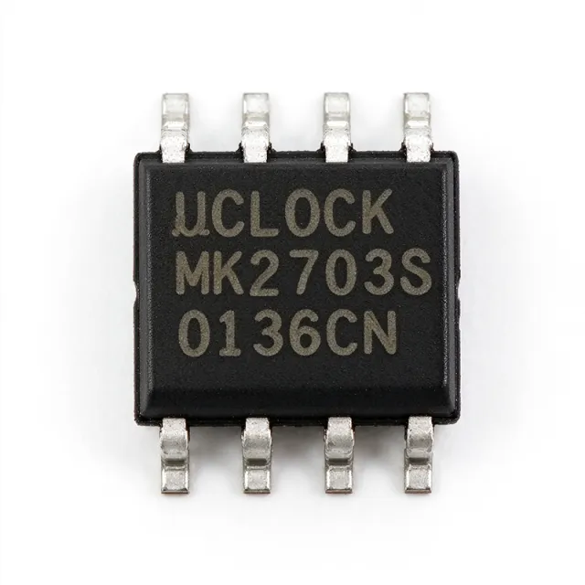
MK2703S - 27MHz PLL Clock Synthesizer | Renesas
MK2703S

MK2703S - 27MHz PLL Clock Synthesizer | Renesas

The Renesas Electronics MK2703S is a 27MHz PLL clock synthesizer IC designed for low-cost, low-jitter clock generation in set-top box and multimedia systems, supplied in an 8-pin SOIC surface-mount package. It operates from 3.13V to 5.5V and is identified by distributor listings as a PLL clock synthesizer with one clock output. A PLL clock synthesizer is a timing IC that uses a phase-locked loop to generate or distribute a stable reference clock for digital and multimedia systems. In the broader electronics hierarchy, the MK2703S belongs to clock and timing integrated circuits, alongside clock generators, frequency dividers, PLL multipliers, and clock buffers. Its purpose is to replace discrete oscillator and PLL circuitry with a compact integrated solution. The verified product data identifies the MK2703S as a low-cost, low-jitter, high-performance PLL clock synthesizer for set-top boxes and multimedia equipment. Its specified 27MHz operating frequency provides a centralized timing reference for system logic, while the 3.13V to 5.5V supply range accommodates common embedded and consumer electronics rails. The 8-SOIC package supports conventional surface-mount assembly and reduces board area compared with discrete oscillator networks. The part is offered in tube packaging according to the verified distributor listing, and distributor records also identify it as a PLL clock synthesizer IC with a 1-output configuration. Exact jitter, phase noise, lock-time, output-drive, and reference-input details were not included in the supplied web excerpts and therefore require confirmation from the manufacturer datasheet before production release. Those unspecified values are important when evaluating a replacement or a new board design. Typical uses include set-top box timing, multimedia processor clocks, digital media modules, and compact consumer systems requiring a single synthesized clock. The MK2703S can replace a discrete oscillator and PLL implementation, but the reference clock source, loop-filter network, output load, and decoupling requirements must follow the manufacturer application guidance. The verified source describes the device as intended to replace oscillators and PLL circuits, while the operating conditions and package details define the core procurement and integration constraints. For a new design, begin with the official Renesas MK27033 datasheet and verify the complete pinout, recommended reference configuration, and electrical limits before layout. Distributor search data confirms the 27MHz device, SOIC-8 package, and supply range, but it does not provide enough detail to reconstruct the full application circuit. Pricing, stock, and lifecycle status should also be checked against current distributor records at the time of purchase. This product summary combines verified distributor attributes with the manufacturer datasheet resource, while clearly separating known electrical facts from parameters requiring datasheet confirmation. It is useful for initial sourcing, clock-tree architecture review, and identifying whether the MK2703S belongs in a candidate design, but it is not a substitute for the complete manufacturer datasheet.

견적 요청 문의하기
MK2703SI - Low-Jitter PLL Audio Clock Synthesizer | Renesas
MK2703SI

MK2703SI - Low-Jitter PLL Audio Clock Synthesizer | Renesas

The Renesas Electronics MK2703SI is a low-cost, low-jitter PLL audio clock synthesizer designed to replace discrete oscillator and PLL circuits in set-top box and multimedia systems. The verified source material identifies it as an 8-SOIC device with a 0.154 inch, 3.90 mm package width. The available data does not provide a verified output-frequency list, input-frequency range, supply voltage, current consumption, pin mapping, or exact operating-temperature values, so those parameters remain design-review items. A PLL audio clock synthesizer is a clock-and-timing IC that uses a phase-locked loop to generate or distribute one or more timing signals with controlled frequency relationships. In the broader electronics hierarchy, it belongs to clock generation, frequency synthesis, PLL, timing IC, and digital signal-support categories. This makes the MK2703SI relevant where audio, multimedia, or embedded systems need a stable reference or derived clock instead of a collection of separate oscillators and divider logic. The manufacturer search results identify the MK2703 family as a PLL audio clock synthesizer and specifically describe the device as a low-cost, low-jitter, high-performance alternative to oscillator and PLL circuits. The SI ordering suffix is associated with an 8-SOIC package in the verified distributor result. Because the supplied web data does not expose the complete electrical specification table, designers should verify frequency generation modes, reference requirements, output drive, supply limits, decoupling, and signal integrity against the official Renesas MK2703 datasheet before layout release. The MK2703SI can be considered for set-top box clocking, multimedia-system timing, audio-clock generation, decoder reference clocks, and embedded multimedia platforms. In a typical implementation, the device would receive a reference signal and produce one or more derived clocks required by downstream processors, converters, or audio circuitry. The main design trade-offs are package footprint, supported output frequencies, jitter, reference quality, supply noise, and whether the required clock architecture matches the device's verified control interface. Use the official MK2703 datasheet as the controlling source for pin names, timing diagrams, electrical limits, recommended crystals or oscillators, and application examples. Do not infer a pinout from the 8-SOIC package alone. In particular, verify every unused or no-connect pin, the exposed thermal requirements, the required supply bypass capacitors, and the maximum operating frequency before substituting the part into an existing design. This page consolidates the verified distributor identity, package information, family description, datasheet links, sourcing context, and engineering caveats for MK2703SI. It also distinguishes confirmed facts from parameters that still require datasheet verification, helping engineers identify the correct next step without presenting unverified clock or electrical values as specifications.

견적 요청 문의하기
MK2703SILF - 27MHz PLL Audio Clock Synthesizer | Renesas
MK2703SILF

MK2703SILF - 27MHz PLL Audio Clock Synthesizer | Renesas

The Renesas Electronics MK2703SILF is a PLL audio clock synthesizer operating from a 27 MHz crystal or clock input, with a supply range of 3.13 V to 5.5 V, in an 8-pin SOIC package measuring 3.90 mm wide. Designed to replace discrete oscillators and PLL circuits, it generates a buffered reference clock and a selectable audio clock for set-top box and multimedia systems. A PLL clock synthesizer is a clock-and-timing IC that multiplies or divides a stable input reference to produce one or more synchronized output frequencies. In the broader semiconductor hierarchy, the MK2703 belongs to the PLL multiplier/divider family, the clock generator and synthesizer class, and ultimately the clock-and-timing integrated-circuit category. Its low-cost integration reduces component count and simplifies clock-tree construction compared with separate crystal oscillators, dividers, and phase-locked-loop circuitry. The verified product information identifies the MK2703SILF as a 27 MHz single PLL clock synthesizer with an 8-pin SOIC surface-mount package. It accepts a 3.13 V to 5.5 V operating supply and provides a buffered reference output together with a selectable audio clock. These functions are useful when downstream converters, codecs, interface circuits, or digital signal processors require a derived clock that remains phase-related to the system reference. Technically, the device uses analog phase-locked-loop techniques to lock an internally controlled output to the external 27 MHz reference. Locking the synthesized clock to the same reference used by the rest of the system can improve timing consistency, while the selectable output division allows a practical audio-clock rate to be produced without a separate programmable synthesizer. Because the supplied web data does not enumerate every programmable frequency, jitter value, output format, or loop filter setting, those details must be confirmed in the manufacturer datasheet before final clock-tree validation. Typical uses include set-top box clock trees, multimedia receivers, DVD and digital-audio equipment, network equipment requiring stable derived clocks, and embedded audio systems where a single reference must feed several clock domains. The device is also appropriate for industrial control equipment when its specified operating range, electrical limits, and environmental qualifications match the system requirements. When laying out an MK2703SILF design, place the device and its associated crystal or clock-source components close to the circuit being clocked, keep output routes short, and provide return paths that do not share high-current switching paths. Confirm crystal load capacitance, output series termination, supply bypassing, and all supported output frequencies from the manufacturer datasheet before production release. This product record combines verified distributor and manufacturer information, traceable source links, honest specification gaps, and engineering-oriented application guidance. It distinguishes documented facts from parameters that still require verification, helping engineers evaluate the MK2703SILF without treating incomplete distributor summaries as a complete electrical datasheet.

견적 요청 문의하기
MK2703SILFTR - 27MHz PLL Audio Clock Synthesizer | Renesas (Tape & Reel)
MK2703SILFTR

MK2703SILFTR - 27MHz PLL Audio Clock Synthesizer | Renesas (Tape & Reel)

The Renesas Electronics MK2703SILFTR is a PLL audio clock synthesizer operating from a 27 MHz crystal or clock input, with a supply range of 3.13 V to 5.5 V, in an 8-pin SOIC package measuring 3.90 mm wide. Designed to replace discrete oscillators and PLL circuits, it generates a buffered reference clock and a selectable audio clock for set-top box and multimedia systems. A PLL clock synthesizer is a clock-and-timing IC that multiplies or divides a stable input reference to produce one or more synchronized output frequencies. In the broader semiconductor hierarchy, the MK2703 belongs to the PLL multiplier/divider family, the clock generator and synthesizer class, and ultimately the clock-and-timing integrated-circuit category. Its low-cost integration reduces component count and simplifies clock-tree construction compared with separate crystal oscillators, dividers, and phase-locked-loop circuitry. The verified product information identifies the MK2703SILFTR as a 27 MHz single PLL clock synthesizer with an 8-pin SOIC surface-mount package. It accepts a 3.13 V to 5.5 V operating supply and provides a buffered reference output together with a selectable audio clock. These functions are useful when downstream converters, codecs, interface circuits, or digital signal processors require a derived clock that remains phase-related to the system reference. Technically, the device uses analog phase-locked-loop techniques to lock an internally controlled output to the external 27 MHz reference. Locking the synthesized clock to the same reference used by the rest of the system can improve timing consistency, while the selectable output division allows a practical audio-clock rate to be produced without a separate programmable synthesizer. Because the supplied web data does not enumerate every programmable frequency, jitter value, output format, or loop filter setting, those details must be confirmed in the manufacturer datasheet before final clock-tree validation. Typical uses include set-top box clock trees, multimedia receivers, DVD and digital-audio equipment, network equipment requiring stable derived clocks, and embedded audio systems where a single reference must feed several clock domains. The device is also appropriate for industrial control equipment when its specified operating range, electrical limits, and environmental qualifications match the system requirements. When laying out an MK2703SILFTR design, place the device and its associated crystal or clock-source components close to the circuit being clocked, keep output routes short, and provide return paths that do not share high-current switching paths. Confirm crystal load capacitance, output series termination, supply bypassing, and all supported output frequencies from the manufacturer datasheet before production release. This product record combines verified distributor and manufacturer information, traceable source links, honest specification gaps, and engineering-oriented application guidance. It distinguishes documented facts from parameters that still require verification, helping engineers evaluate the MK2703SILFTR without treating incomplete distributor summaries as a complete electrical datasheet.

견적 요청 문의하기
MK2703SITR - Low-Jitter PLL Audio Clock Synthesizer | Renesas (Tape & Reel)
MK2703SITR

MK2703SITR - Low-Jitter PLL Audio Clock Synthesizer | Renesas (Tape & Reel)

The Renesas Electronics MK2703SITR is a low-cost, low-jitter PLL audio clock synthesizer designed to replace discrete oscillator and PLL circuits in set-top box and multimedia systems. The verified source material identifies it as an 8-SOIC device with a 0.154 inch, 3.90 mm package width. The available data does not provide a verified output-frequency list, input-frequency range, supply voltage, current consumption, pin mapping, or exact operating-temperature values, so those parameters remain design-review items. A PLL audio clock synthesizer is a clock-and-timing IC that uses a phase-locked loop to generate or distribute one or more timing signals with controlled frequency relationships. In the broader electronics hierarchy, it belongs to clock generation, frequency synthesis, PLL, timing IC, and digital signal-support categories. This makes the MK2703SITR relevant where audio, multimedia, or embedded systems need a stable reference or derived clock instead of a collection of separate oscillators and divider logic. The manufacturer search results identify the MK2703 family as a PLL audio clock synthesizer and specifically describe the device as a low-cost, low-jitter, high-performance alternative to oscillator and PLL circuits. The SI ordering suffix is associated with an 8-SOIC package in the verified distributor result. Because the supplied web data does not expose the complete electrical specification table, designers should verify frequency generation modes, reference requirements, output drive, supply limits, decoupling, and signal integrity against the official Renesas MK2703 datasheet before layout release. The MK2703SITR can be considered for set-top box clocking, multimedia-system timing, audio-clock generation, decoder reference clocks, and embedded multimedia platforms. In a typical implementation, the device would receive a reference signal and produce one or more derived clocks required by downstream processors, converters, or audio circuitry. The main design trade-offs are package footprint, supported output frequencies, jitter, reference quality, supply noise, and whether the required clock architecture matches the device's verified control interface. Use the official MK2703 datasheet as the controlling source for pin names, timing diagrams, electrical limits, recommended crystals or oscillators, and application examples. Do not infer a pinout from the 8-SOIC package alone. In particular, verify every unused or no-connect pin, the exposed thermal requirements, the required supply bypass capacitors, and the maximum operating frequency before substituting the part into an existing design. This page consolidates the verified distributor identity, package information, family description, datasheet links, sourcing context, and engineering caveats for MK2703SITR. It also distinguishes confirmed facts from parameters that still require datasheet verification, helping engineers identify the correct next step without presenting unverified clock or electrical values as specifications.

견적 요청 문의하기

MK2703SLF - 27MHz Low-Jitter PLL Clock Synthesizer | Renesas
MK2703SLF

MK2703SLF - 27MHz Low-Jitter PLL Clock Synthesizer | Renesas

The Renesas Electronics MK2703SLF is a low-cost, low-jitter PLL audio clock synthesizer built around a 27 MHz crystal or clock reference and supplied in an 8-pin SOIC package. It provides a buffered reference clock and a selectable audio clock for set-top boxes, multimedia systems, and other digital audio equipment. The verified distributor listing identifies the device as a PLL clock synthesizer IC with one 27 MHz clock input and an 8-SOIC package measuring 0.154 inches wide by 3.90 mm. A PLL clock synthesizer is a clock-and-timing integrated circuit that uses phase-locked-loop technology to derive stable digital clock outputs from a reference oscillator. In the broader hierarchy, it belongs to clock generation, frequency synthesis, timing ICs, and integrated circuits rather than a general-purpose oscillator or analog signal source. Its role is to distribute and transform timing signals so that audio, communication, and multimedia subsystems can operate from a controlled reference. The MK2703 family uses a low-cost analog PLL approach and is intended to replace discrete oscillator and PLL circuitry. According to the available manufacturer and distributor descriptions, the device accepts a 27 MHz crystal or clock input, produces a buffered reference clock, and offers a selectable audio clock. The verified material does not provide the complete output-frequency table, phase-noise figures, supply-voltage range, or pin-level timing values, so those specifications remain marked for data acquisition rather than being inferred. Typical applications include set-top boxes, DVD and multimedia systems, audio-clock generation, digital entertainment equipment, and embedded consumer electronics. The selectable audio output is useful when a downstream audio converter or digital interface requires a controlled clock. The buffered reference output can provide a cleaner system timing source than leaving the crystal oscillator unloaded, subject to the device's specified load and output-drive requirements. The principal design consideration is verifying the exact crystal frequency, supported divider or feedback settings, output jitter, supply requirements, and pinout against the complete MK2703 datasheet before layout. In a new design, preserve the manufacturer's recommended decoupling and crystal-load network and confirm that the selected SOIC footprint matches the board. This device is best suited to designs that specifically need its documented clock architecture rather than a general high-performance frequency synthesizer.

견적 요청 문의하기
MK2703SLFTR - 27MHz Low-Jitter PLL Clock Synthesizer | Renesas (Tape & Reel)
MK2703SLFTR

MK2703SLFTR - 27MHz Low-Jitter PLL Clock Synthesizer | Renesas (Tape & Reel)

The Renesas Electronics MK2703SLFTR is a low-cost, low-jitter PLL audio clock synthesizer built around a 27 MHz crystal or clock reference and supplied in an 8-pin SOIC package. It provides a buffered reference clock and a selectable audio clock for set-top boxes, multimedia systems, and other digital audio equipment. The verified distributor listing identifies the device as a PLL clock synthesizer IC with one 27 MHz clock input and an 8-SOIC package measuring 0.154 inches wide by 3.90 mm. A PLL clock synthesizer is a clock-and-timing integrated circuit that uses phase-locked-loop technology to derive stable digital clock outputs from a reference oscillator. In the broader hierarchy, it belongs to clock generation, frequency synthesis, timing ICs, and integrated circuits rather than a general-purpose oscillator or analog signal source. Its role is to distribute and transform timing signals so that audio, communication, and multimedia subsystems can operate from a controlled reference. The MK2703 family uses a low-cost analog PLL approach and is intended to replace discrete oscillator and PLL circuitry. According to the available manufacturer and distributor descriptions, the device accepts a 27 MHz crystal or clock input, produces a buffered reference clock, and offers a selectable audio clock. The verified material does not provide the complete output-frequency table, phase-noise figures, supply-voltage range, or pin-level timing values, so those specifications remain marked for data acquisition rather than being inferred. Typical applications include set-top boxes, DVD and multimedia systems, audio-clock generation, digital entertainment equipment, and embedded consumer electronics. The selectable audio output is useful when a downstream audio converter or digital interface requires a controlled clock. The buffered reference output can provide a cleaner system timing source than leaving the crystal oscillator unloaded, subject to the device's specified load and output-drive requirements. The principal design consideration is verifying the exact crystal frequency, supported divider or feedback settings, output jitter, supply requirements, and pinout against the complete MK2703 datasheet before layout. In a new design, preserve the manufacturer's recommended decoupling and crystal-load network and confirm that the selected SOIC footprint matches the board. This device is best suited to designs that specifically need its documented clock architecture rather than a general high-performance frequency synthesizer.

견적 요청 문의하기
MK2703STR - 27MHz PLL Audio Clock Synthesizer | Renesas
MK2703STR

MK2703STR - 27MHz PLL Audio Clock Synthesizer | Renesas

The Renesas Electronics MK2703STR is a 27MHz PLL audio clock synthesizer IC designed to provide stable low-jitter clocking for audio and multimedia equipment. It operates as a PLL clock synthesizer with bypass capability and accepts a clock or crystal input while providing a CMOS output. The device is supplied in an 8-SOIC package measuring 0.154 inches, or 3.90mm, in width. A PLL clock synthesizer is a clock-generation and timing component that compares an input reference with an internal feedback signal, locks a phase-locked loop, and produces one or more stable output frequencies. In the broader electronics hierarchy, the MK2703STR belongs to the clock and timing IC category and supports systems where predictable audio-frequency generation is required. Its bypass function is useful when the system needs a direct clock path during specific operating conditions. The verified listing identifies the MK2703STR as a low-cost, low-jitter, high-performance PLL clock synthesizer intended to replace discrete oscillator and PLL circuits in set-top box and multimedia systems. The specified maximum frequency is 27MHz, and the listed input/output ratio is 2:2. The CMOS output supports integration with digital audio, consumer multimedia, and related embedded systems where a standardized clock source is advantageous. The 8-SOIC package is suitable for conventional surface-mount PCB assembly and provides a compact implementation for consumer equipment. Because the supplied verified data does not state the complete electrical limits, pin names, supply voltage, jitter value, or crystal-load details, those parameters should be confirmed in the Renesas MK2703 datasheet before schematic capture or production release. Typical uses include digital audio clocking, set-top box clock generation, multimedia system timing, and other consumer electronics requiring a low-jitter PLL-based reference. In these applications, the device can simplify clock distribution by consolidating oscillator and feedback functions into one timing IC, although the final bill of materials still depends on the required frequency, output format, and system clock tree. Designers should place the IC and its decoupling connections according to the manufacturer layout guidance, preserve the recommended crystal or reference network, and verify output jitter and lock behavior over the intended supply and temperature range. This page summarizes verified distributor and manufacturer references while clearly separating unavailable parameters from confirmed facts.

USD $1.97 문의하기
MK2704S - 36.864MHz PLL Audio Clock Synthesizer | Renesas
MK2704S

MK2704S - 36.864MHz PLL Audio Clock Synthesizer | Renesas

The Renesas Electronics MK2704S is a low-cost, low-jitter PLL audio clock synthesizer with a maximum frequency of 36.864MHz, selectable clock or crystal input, CMOS output, and PLL bypass capability, housed in an 8-pin SOIC package. It is designed to consolidate oscillator and PLL functions in multimedia systems and set-top boxes. A PLL clock synthesizer multiplies or organizes a reference clock into a stable operating or audio sampling clock. In the signal path, it belongs to clock and timing ICs, where its role is to generate predictable digital timing from a crystal or external reference. The available ratio of 1:2 indicates that this device family is intended for a defined clock-generation relationship rather than general-purpose fractional-N synthesis. Key verified features include PLL operation with bypass, clock or crystal input, one clock circuit, and a CMOS output. The bypass path is useful during startup, test, or mode transitions, while the PLL path supports synthesized clock generation. The 36.864MHz maximum frequency makes the device applicable to multimedia timing systems operating around common digital audio-related clock domains, subject to the complete manufacturer datasheet limits. The MK2704S uses a single 8-pin SOIC package according to the available distributor records. The package supports conventional surface-mount assembly and can simplify board replacement compared with discrete oscillator-plus-divider assemblies. Its architecture is intended to replace separate oscillator and PLL circuits in set-top box and multimedia equipment, reducing board count while centralizing clock generation. Typical uses include set-top box clock generation, multimedia system timing, digital audio interfaces, and other embedded systems requiring a CMOS clock with bypass control. When designing around the device, verify crystal start-up requirements, output loading, supply voltage, and all operating conditions against the manufacturer datasheet. Because the supplied evidence is distributor-oriented and does not include a complete official parametric table, unverified values are not inferred. This product page combines verified source snippets, application guidance, source links, and engineering caveats rather than inventing electrical ratings. It distinguishes known specifications from fields that require confirmation in the manufacturer datasheet, helping engineers identify the MK2704S quickly while avoiding unsupported claims.

견적 요청 문의하기
MK2704SLF PLL Audio Clock Synthesizer | Renesas
MK2704SLF

MK2704SLF PLL Audio Clock Synthesizer | Renesas

Renesas MK2704SLF is a PLL audio clock synthesizer integrated circuit in an 8-pin SOIC package. Verified source data identifies the device as a single PLL clock synthesizer for audio or other clock-generation applications, with a commercial temperature grade, gull-wing leads, and eight terminals. The available evidence confirms the component family, package class, and clock-generation function, while detailed frequency, supply-voltage, output, jitter, and pin-level data require the manufacturer datasheet. A PLL clock synthesizer is a clock-generation and timing IC that uses a phase-locked loop to derive, divide, multiply, or distribute a stable clock relationship from a reference source. In audio systems, such devices can support sampling-clock generation, clock conversion, and distribution where a stable reference is needed across multiple signal paths. The Renesas MK2704SLF belongs to the clock generator, PLL, and frequency-synthesizer category. The verified listing describes the MK2704SLF as a PLL audio clock synthesizer and identifies an 8-SOIC package measuring approximately 3.90 mm wide. The package uses a gull-wing terminal form and is listed as commercial grade. Because the supplied source excerpts do not include the complete manufacturer specification table, no operating-frequency range, supply-voltage limits, output configuration, phase-noise value, or jitter figure is inferred here. Typical design use includes audio-clock generation, digital-audio equipment, interface clocking, and other embedded systems requiring a PLL-based clock source. In these systems, the clock quality affects synchronization between converters, processors, serializers, and digital signal processors. A designer should compare the complete datasheet limits against the system reference frequency, required output frequency, load, supply voltage, temperature range, and downstream timing budget before production release. The most important implementation consideration is to follow the exact pinout, recommended decoupling, input/output termination, and grounding arrangement in the manufacturer datasheet. Do not substitute an electrically similar clock IC solely by package count; PLL architecture, reference frequency, output format, and enable behavior must be verified. This page combines verified distributor metadata, package information, sourcing links, and design guidance without filling unverified parameters with assumptions. This product page is useful for engineers identifying an MK2704SLF, locating its datasheet, checking its SOIC-8 format, and beginning a controlled replacement or sourcing review. Exact electrical and timing specifications should be confirmed against the current Renesas documentation before schematic release.

견적 요청 문의하기
MK2704SLFTR PLL Audio Clock Synthesizer | Renesas (Tape & Reel)
MK2704SLFTR

MK2704SLFTR PLL Audio Clock Synthesizer | Renesas (Tape & Reel)

Renesas MK2704SLFTR is a PLL audio clock synthesizer integrated circuit in an 8-pin SOIC package. Verified source data identifies the device as a single PLL clock synthesizer for audio or other clock-generation applications, with a commercial temperature grade, gull-wing leads, and eight terminals. The available evidence confirms the component family, package class, and clock-generation function, while detailed frequency, supply-voltage, output, jitter, and pin-level data require the manufacturer datasheet. A PLL clock synthesizer is a clock-generation and timing IC that uses a phase-locked loop to derive, divide, multiply, or distribute a stable clock relationship from a reference source. In audio systems, such devices can support sampling-clock generation, clock conversion, and distribution where a stable reference is needed across multiple signal paths. The Renesas MK2704SLFTR belongs to the clock generator, PLL, and frequency-synthesizer category. The verified listing describes the MK2704SLFTR as a PLL audio clock synthesizer and identifies an 8-SOIC package measuring approximately 3.90 mm wide. The package uses a gull-wing terminal form and is listed as commercial grade. Because the supplied source excerpts do not include the complete manufacturer specification table, no operating-frequency range, supply-voltage limits, output configuration, phase-noise value, or jitter figure is inferred here. Typical design use includes audio-clock generation, digital-audio equipment, interface clocking, and other embedded systems requiring a PLL-based clock source. In these systems, the clock quality affects synchronization between converters, processors, serializers, and digital signal processors. A designer should compare the complete datasheet limits against the system reference frequency, required output frequency, load, supply voltage, temperature range, and downstream timing budget before production release. The most important implementation consideration is to follow the exact pinout, recommended decoupling, input/output termination, and grounding arrangement in the manufacturer datasheet. Do not substitute an electrically similar clock IC solely by package count; PLL architecture, reference frequency, output format, and enable behavior must be verified. This page combines verified distributor metadata, package information, sourcing links, and design guidance without filling unverified parameters with assumptions. This product page is useful for engineers identifying an MK2704SLFTR, locating its datasheet, checking its SOIC-8 format, and beginning a controlled replacement or sourcing review. Exact electrical and timing specifications should be confirmed against the current Renesas documentation before schematic release.

견적 요청 문의하기