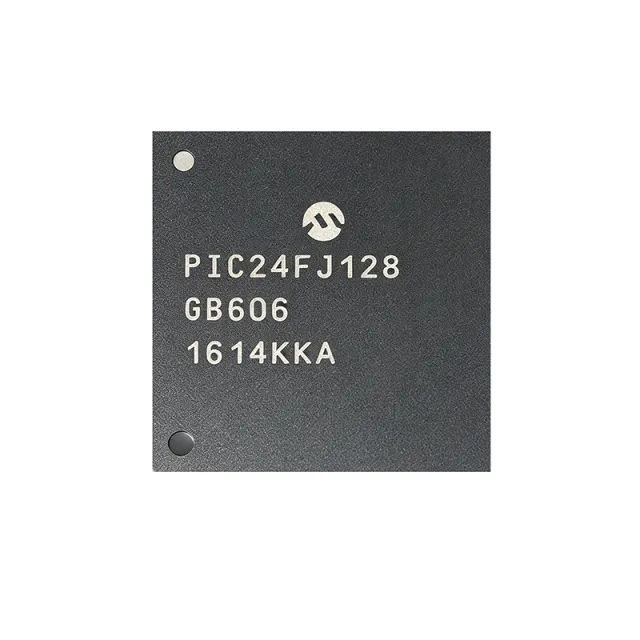
PIC24FJ128GB606-I/MR
PIC24FJ128GB606-I/MR - 16-bit 32MHz 128KB Flash USB MCU | Microchip
The Microchip Technology PIC24FJ128GB606-I/MR is a 16-bit PIC24F microcontroller running up to 32 MHz (16 MIPS), integrating 128 KB dual Flash program memory plus 32 KB RAM, full-speed USB On-The-Go (OTG), and a 53-I/O footprint, all housed in a 64-pin 9x9 mm QFN package. Targeted at low-power USB-embedded designs, it carries on-chip peripherals including 10/12-bit ADC, charge-time measurement unit (CTMU), configurable logic cells (CLC), and live-update Flash partitioning for safe firmware field upgrades.
A microcontroller (MCU) is an integrated circuit that combines a CPU core, program memory (Flash), working memory (RAM), and a configurable set of peripherals such as timers, ADC, communication controllers, and I/O pins, all on a single die. Within the broader semiconductor taxonomy, a PIC24F MCU belongs to the family of 16-bit microcontrollers, which sit above 8-bit MCUs in compute and memory capability but below 32-bit Cortex-M and high-end application processors. PIC24F parts in particular target low-power, USB- or graphics-friendly embedded designs, balancing deterministic 16-MIPS throughput with eXtreme Low Power (XLP) sleep modes.
Key differentiating features of the PIC24FJ128GB606 include dual-bank Flash with Live Update (enabling firmware swap without device reset), 128 KB program Flash (43K x 24 words), 32 KB RAM, full-speed USB 2.0 OTG with on-chip transceiver, 53 general-purpose I/O, peripheral-pinning remapping, multiple serial interfaces (UART, SPI, I2C), a real-time clock calendar (RTCC) with on-chip 32 kHz oscillator, and XLP technology for sub-uA sleep current.
Architecturally, the PIC24FJ128GB606 uses Microchip's 16-bit modified-Harvard core with a 24-bit instruction word, delivering up to 16 MIPS at 32 MHz while operating from a single 2.0 V to 3.6 V supply. The dual-panel Flash memory plus a small boot Flash row supports field firmware updates via Live Update: code can be written to the inactive panel while the active panel continues to run, then a controlled swap is performed - useful for industrial and IoT devices that cannot tolerate shutdown during firmware upgrades. On-chip peripherals are mapped through Peripheral Pin Select (PPS), giving the designer flexibility to assign digital peripherals to a wide range of I/O pins without hardware rework.
Typical applications include USB peripherals (HID, CDC, mass storage, audio class), industrial sensor hubs, portable data loggers, USB-connected human-interface devices, and low-power wireless sensor nodes bridging to external radios. The integrated CTMU makes the device a strong fit for capacitive-touch keypads, time-of-flight measurements, and precision analog front ends using the on-chip 10/12-bit ADC. The 53-I/O count also suits mixed-signal control boards that previously required a 64/80/100-pin PIC24, enabling footprint reduction when migrating a panel to a smaller 64-pin QFN.
Designers should note that the MR suffix indicates a QFN-64 (9x9 mm) package with an exposed thermal pad (EP); the exposed pad must be soldered to a properly sized copper island on the PCB for thermal relief and electrical ground. Power decoupling should follow Microchip's typical-application guidance: 0.1 uF and 1 uF ceramic caps placed within 5 mm of the VDD/VSS pairs, plus a 4.7 uF bulk cap on the main rail. For USB OTG operation, the internal 3.3 V regulator must be enabled and a 1 uF cap placed on the VUSB3V pin per the manufacturer datasheet.
This page synthesizes distributor pricing, drop-in alternatives from Microchip's own 24FJ product family and cross-brand references, and practical design notes not found in the bare datasheet, giving procurement and firmware teams a one-stop reference for the PIC24FJ128GB606-I/MR.
견적 요청
문의하기