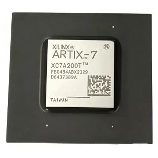
5CGXFC7C7F23C8N - Cyclone V GX FPGA 149.5K LE | Altera
부품 번호: 5CGXFC7C7F23C8N ✓ 활성| 수량 | 단가 | 합계 |
|---|---|---|
| 1 | $0 | $0.00 |
| 10 | $0 | $0.00 |
| 100 | $0 | $0.00 |
| 500 | $0 | $0.00 |
| 1,000 | $0 | $0.00 |
5CGXFC7C7F23C8N 개요
A field-programmable gate array (FPGA) is a semiconductor device containing a fabric of configurable logic blocks, routing resources, and I/O cells that designers program to implement custom digital circuits. FPGAs sit above fixed-function ASICs and ASSPs in the programmable logic hierarchy, offering reconfigurability and shorter time-to-market, and the Cyclone V family specifically targets the lowest system cost and lowest power in Intel/Altera's FPGA portfolio.
Key features of the 5CGXFC7C7F23C8N include 156 variable-precision DSP blocks for fixed- and floating-point arithmetic, 240 user I/O pins supporting multiple I/O standards, and integrated 3.125 Gbps-class transceivers for PCI Express, Serial RapidIO, and other serial protocols. The 'FC' designation indicates the inclusion of hard IP for protocol building blocks, reducing logic utilization and improving timing closure versus soft implementations.
The device is fabricated on TSMC's 28nm low-power (28LP) process, which delivers a favorable logic-density-to-power ratio. The M9K and M144K embedded memory blocks total 7,880,704 RAM bits, sufficient for line buffering, packet processing, and video frame storage without external memories in many designs.
Typical applications include industrial automation and motor drive control, wireless and wireline communications infrastructure, broadcast video processing, and consumer electronics bridging. The transceiver resources fit PCIe endpoint/root-port designs in industrial cards and data acquisition systems.
A key design consideration is power distribution: the 1.1V VCCINT rail must be tightly regulated with adequate bulk and ceramic decoupling, and transceiver power domains (VCCHSSI, VCCL_GX) require dedicated filtering per the Cyclone V power management guidelines. Power estimation should be done in Intel PowerPlay tools before finalizing the regulator design.
This page synthesizes distributor availability data, drop-in same-family alternatives, and practical design notes not found in the manufacturer datasheet, providing selection guidance for engineers comparing Cyclone V GX speed grades and density options.
드롭인 대체품: 5CGXFC7C7F23C8N — 동일 패키지, 핀 호환. PCB 재작업이 필요한 다른 패키지 부품은 제외됩니다.
빠른 비교 도구 — 나란히 비교할 대체 부품을 선택하십시오:
5CGXFC7C7F23C6N
✅ 드롭인 ⚠️ 사양 미검증📋 참조 대체품 (카탈로그에 없음)
5CGXFC7C7F23I7N
✅ 드롭인 ⚠️ 사양 미검증📋 참조 대체품 (카탈로그에 없음)
5CGXFC7D7F23C8N
✅ 드롭인 ⚠️ 사양 미검증📋 참조 대체품 (카탈로그에 없음)
5CGXFC5C7F23C8N
✅ 드롭인 ⚠️ 사양 미검증📋 참조 대체품 (카탈로그에 없음)
5CGXFC9C7F23C8N
✅ 드롭인 ⚠️ 사양 미검증📋 참조 대체품 (카탈로그에 없음)
5CGXFC7C7F23C8N 최대 정격 & 전기적 특성
| Family | Cyclone V GX |
| Logic Elements (LEs) | 149500 |
| Adaptive Logic Modules (ALMs) | 56480 |
| Embedded Memory | 7880704 bit (7.696 Mbit) |
| DSP Blocks (18x18) | 156 |
| Number of I/O | 240 |
| Operating Supply Voltage (Core) | 1.1 V |
| Process Technology | 28 nm (TSMC 28LP) |
| 패키지 / 케이스 | FBGA-484 |
| 장착 스타일 | SMD/SMT |
| Minimum Operating Temperature | 0 C |
| Maximum Operating Temperature | 85 C |
| Speed Grade | C7 (commercial, grade 7) |
| Packaging | Tray |
| Terminal Form | Ball |
5CGXFC7C7F23C8N fbga-484 핀 구성 가이드
5CGXFC7C7F23C8N(fbga-484 패키지)의 핀 구성입니다. 이 디지털 IC에는 GPIO, 통신 인터페이스(UART, SPI, I2C), 전원 핀이 포함되어 있습니다. 대체 핀 기능과 구성 옵션은 제조사 데이터시트를 참조하십시오. 임베디드 시스템 설계와 PCB 레이아웃에 필수적입니다.

다음에 대한 상세 핀아웃 데이터 없음: 5CGXFC7C7F23C8N.
다음을 참조하십시오: 데이터시트 전체 핀 구성은 다음을 참조하십시오.
일반적인 애플리케이션
5CGXFC7C7F23C8N 적합 용도: 6 애플리케이션s: Industrial Motor Drive Control, PCIe Data Acquisition Cards, Broadcast Video Processing, Wireless Baseband and Radio, Medical Imaging Instrumentation, Industrial Automation and PLC Backplane.
Industrial Motor Drive Control
The 5CGXFC7C7F23C8N fits industrial motion and motor-drive control because its 156 DSP blocks execute multi-axis field-oriented control (FOC) loops with deterministic sub-microsecond latency that microcontrollers cannot match. The 149,500-LE fabric hosts multiple PWM generators, quadrature encoders, and safety interlocks concurrently, while the 7.696 Mbit embedded memory buffers current-feedback histories for diagnostics. In a typical topology, ADC interface logic samples phase currents, DSP blocks run Park/Clarke transforms and PI loops, and hardened protocol IP bridges to a plant Ethernet or EtherCAT master via the transceivers. Unlike a DSP-plus-FPGA two-chip solution, integration on one 1.1V, 28nm device reduces BOM cost and board area; the trade-off is that control firmware becomes HDL and requires disciplined timing closure on the C7 speed grade.
추천
PCIe Data Acquisition Cards
For industrial and instrument data-acquisition (DAQ) cards, the 5CGXFC7C7F23C8N pairs its hardened PCI Express IP with the 149,500-LE fabric to implement DMA engines, channel aggregation, and real-time filtering without soft-IP protocol overhead. The integrated multi-gigabit transceivers connect directly to the PCIe edge-finger differential pairs, and the 7,880,704-bit embedded memory stages burst data between the host and converter front ends. A common architecture uses the fabric to frame ADC samples into descriptors, DMA engines to saturate the link, and DSP blocks to apply per-channel FIR decimation. Placing the FPGA within short trace lengths of the edge connector with the specified transceiver reference-clock and decoupling network preserves eye margin; at a 3.125 Gbps-class rate, the C7 grade closes timing with margin in typical Gen1/Gen2 designs.
추천
Broadcast Video Processing
Broadcast equipment such as frame synchronizers, format converters, and 3G-SDI processing cards suits the 5CGXFC7C7F23C8N because its 7.696 Mbit of embedded M9K/M144K memory holds multiple HD line buffers on-chip, and the 149,500 LEs implement color-space conversion, scaling, and genlock processing in parallel datapaths. The 156 DSP blocks accelerate fixed-point video filters (upsampling, sharpening) that would exhaust smaller fabrics. The transceivers interface to SDI serializer/deserializer companions or drive Ethernet-based SMPST 2110 bridges with the hard protocol IP. In a typical design, video enters through deserializer logic, is processed line-by-line through pipelined stages clocked at the pixel rate, and exits through the transmit path; the C7 speed grade provides adequate Fmax for 1080p60 pipelines, while the 240 I/O support dual-link front ends.
추천
Wireless Baseband and Radio
Small-cell and software-defined-radio (SDR) platforms use the 5CGXFC7C7F23C8N for digital front-end processing: digital up/down conversion, filtering, and crest-factor reduction map naturally onto the 156 DSP blocks, while the transceivers carry JESD204-class or CPRI-style serial links to data converters and radio units. The 149,500-LE fabric implements MAC-layer framing and timing counters disciplined by GPS or IEEE 1588 inputs, and the 7.696 Mbit memory buffers burst traffic between the radio and backhaul. Operating the 28nm fabric at 1.1V keeps baseband power acceptable for compact outdoor units; the key consideration is transceiver jitter hygiene - a low-noise reference clock and the recommended VCCL_GX filtering network are mandatory to meet the serializer phase-noise budget at multi-gigabit rates in the field.
추천
Medical Imaging Instrumentation
Ultrasound beamforming and detector front ends benefit from the 5CGXFC7C7F23C8N because beam-summing hundreds of channels requires exactly the massive parallel multiply-accumulate throughput that 156 DSP blocks provide, sustaining sample streams no embedded CPU can process in real time. The 149,500 LEs implement per-channel time-gain compensation, aperture control, and transmit sequencing, while the 7,880,704-bit embedded memory forms line buffers feeding scan-conversion logic. The 240 I/O pins fan out to high-channel-count ADC banks, and transceivers move processed frames to a host over PCIe using the hard IP. The commercial 0C to 85C rating fits controlled clinical environments; systems needing conduction-cooled or extended-range operation should instead specify the pin-identical industrial 5CGXFC7C7F23I7N variant at design time.
추천
Industrial Automation and PLC Backplane
Programmable-logic-controller (PLC) backplane bridges and machine-vision interface cards adopt the 5CGXFC7C7F23C8N to concentrate many field protocols on one chip: PROFINET, EtherCAT, or EtherNet/IP industrial Ethernet stacks run beside hardened PCIe/serial links, with the 149,500-LE fabric providing the I/O scan engine and deterministic task scheduler. The 7.696 Mbit memory holds process-image tables and non-volatile configuration staging, and the 240 I/O connect parallel fieldbus PHYs and digital I/O banks. Its lowest-power 28nm Cyclone V implementation suits fanless DIN-rail and cabinet-mounted hardware where convection cooling limits dissipation. Designers should budget the multi-rail power tree (1.1V core plus I/O banks) and use the hard IP rather than soft protocol cores to preserve timing margin on the C7 grade across the full 0C to 85C range.
추천
추천 제품 요약
엔지니어링 참조 데이터: 5CGXFC7C7F23C8N — 비교, 설계 지침 및 규정 준수 정보.
선택 가이드
대체품과의 비교
| 파라미터 | 이 제품 | 5CGXFC7C7F23C6N | 5CGXFC7C7F23I7N | 5CGXFC7D7F23C8N | 5CGXFC5C7F23C8N | 5CGXFC9C7F23C8N |
|---|---|---|---|---|---|---|
| Package | FBGA-484 | FBGA-484 - same | FBGA-484 - same | FBGA-484 - same | FBGA-484 - same | FBGA-484 - same |
| Brand | Altera | Altera | Altera | Altera | Altera | Altera |
| Speed Grade | C7 | C6 (faster) | I7 (industrial, grade 7) | C7 | C7 | C7 |
| Temperature Range | 0C to 85C | 0C to 85C | -40C to +100C | 0C to 85C | 0C to 85C | 0C to 85C |
| Core Supply Voltage | 1.1 V | 1.1 V | 1.1 V | 1.1 V | 1.1 V | 1.1 V |
주요 차별점
- Hard protocol IP (FC variant) (vs 5CGXC7C7F23C8N)
- Fastest drop-in timing upgrade (vs 5CGXFC7C7F23C6N)
- Extended temperature option on same die (vs 5CGXFC7C7F23I7N)
설계 노트
The 5CGXFC7C7F23C8N requires a multi-rail power tree: 1.1V VCCINT core, plus separate rails for I/O banks (1.2V-3.0V per standard), transceiver domains (VCCL_GX/VCCHSSI), PLL, and configuration. Use the Intel PowerPlay Early Power Estimator with your actual utilization to size each regulator; FPGA core current scales strongly with clock frequency and toggle rate. Sequence rails per the Cyclone V handbook power-ramp requirements, and provide bulk plus 0.1uF ceramic decoupling at every supply ball group per the Cyclone V pin connection guidelines.
Transceiver links (PCIe, serial backhaul) demand strict reference-clock hygiene: a low-phase-noise oscillator, series termination at the FPGA clock input, and the recommended VCCL_GX filtering network (ferrite plus capacitor bank) to isolate transceiver supply noise. Route transceiver differential pairs with controlled impedance (85 or 100 ohm as required), length-matched within the tolerance given in the Cyclone V pin-out and SI guidelines, and keep them away from switching regulator nodes. Simulate eye margin at your target rate before committing the stackup.
The FBGA-484 escape pattern needs via-in-pad or dogbone escapes on a 0.8 mm-class ball pitch; plan at least one buried-via layer pair for power and fanout. Follow the Intel Cyclone V pin connection guidelines exactly for shared-bank voltage planning - mixing incompatible I/O standards in one bank is the most common layout rework cause. Reserve configuration device connections (AS/QSPI) and JTAG header access on the board even if you plan remote update, to keep factory bring-up and field recovery possible.
Do not assume the C7 speed grade closes timing for every design: run Quartus TimeQuest at the worst commercial corner (0C, 1.07V if applicable) before locking the C8N OPN into production. Designs with marginal slack should qualify the pin-compatible C6 (5CGXFC7C7F23C6N) as a second source or upgrade path. Also verify the exact transceiver count for your target protocol in the Cyclone V device datasheet, since usable lanes in the F23 package depend on which transceiver banks are bonded out.
규정 준수 정보
Compliance statements were not included in the retrieved web data; confirm RoHS/REACH status on the Altera product page or the distributor compliance certificate before procurement.