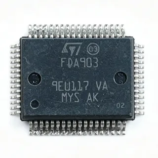
FDA903U - 1A, 35V Ultra-Low Noise LDO | Texas Instruments
부품 번호: FDA903U ✓ 활성| 수량 | 단가 | 합계 |
|---|---|---|
| 1 | $4.85 | $4.85 |
| 10 | $4.36 | $43.60 |
| 100 | $3.88 | $388.00 |
| 500 | $3.49 | $1,745.00 |
| 1,000 | $3.1 | $3,100.00 |
FDA903U 개요
An LDO (Low-Dropout) linear regulator is a type of voltage regulator that maintains a stable output voltage even when the input voltage is very close to the output voltage. It is a key component in power management ICs, providing clean, low-noise power rails for sensitive analog and digital circuits. LDOs are essential in applications where switching noise from DC-DC converters would degrade performance, such as in audio, RF, and precision measurement systems.
Key features include 4.17 uVrms output noise (20 Hz to 100 kHz), 72 dB PSRR at 1 kHz, and a low dropout voltage of 200 mV at full 1A load. The device also offers 6.4 mA quiescent current, an active-high enable pin for power sequencing, and thermal shutdown protection. The VQFN-20 package provides a thermal resistance of 31.4 C/W, enabling compact designs without external heatsinking at moderate power levels.
The FDA903U utilizes a bipolar architecture with a precision bandgap reference, achieving noise performance comparable to discrete reference designs while maintaining regulator simplicity. The high PSRR minimizes ripple from upstream switching converters, making it suitable for noise-sensitive analog and RF signal chains where clean power rails are critical.
Typical applications include high-end audio DAC power supplies, PLL/VCO power rails in RF transceivers, precision ADC/DAC reference buffering, and test and measurement instrumentation. The wide input range also supports industrial 24V bus systems with adequate headroom.
When designing with this device, ensure adequate input-to-output voltage headroom to maintain regulation under all load conditions. The enable pin allows sequential power-up in multi-rail systems, which is essential for processors requiring specific rail sequencing.
드롭인 대체품: FDA903U — 동일 패키지, 핀 호환. PCB 재작업이 필요한 다른 패키지 부품은 제외됩니다.
이 시리즈의 변형
다음과 드롭인 호환되는 동일 시리즈 모델: FDA903U (동일 폼 팩터 및 풋프린트) — 차이점: Package, Enable Pin, Input Voltage Range, MSL Level, Output Type.
빠른 비교 도구 — 나란히 비교할 대체 부품을 선택하십시오:
TPS7A4700RGWR
✅ 드롭인✓ 재고 있음
$3.6591 / 개
데이터시트 보기 →TPS7A4701RGWR-Q1
✅ 드롭인📋 참조 대체품 (카탈로그에 없음)
TPS7A4701RGWT
✅ 드롭인📋 참조 대체품 (카탈로그에 없음)
LT3045EDC
✅ 드롭인 ⚠️ 사양 미검증📋 참조 대체품 (카탈로그에 없음)
ADM7150ARDZ
✅ 드롭인 ⚠️ 사양 미검증📋 참조 대체품 (카탈로그에 없음)
FDA903U 최대 정격 & 전기적 특성
| 출력 유형 | Adjustable |
| 출력 전압 범위 | 1.4 V to 34 V |
| 최대 출력 전류 | 1 A |
| 입력 전압 범위 | 3 V to 35 V |
| 드롭아웃 전압 | 200 mV at 1 A |
| 출력 노이즈 | 4.17 uVrms (20 Hz to 100 kHz) |
| PSRR | 72 dB at 1 kHz |
| 대기 전류 | 6.4 mA |
| 열 저항 | 31.4 C/W |
| 동작 온도 | -40C to +125C |
| 패키지 | VQFN-20 (RGW) 5x5 mm |
| 실장 유형 | Surface Mount |
| MSL 레벨 | 2 (1 year) |
| RoHS 상태 | Compliant |
| 인에이블 핀 | Yes (active-high) |
FDA903U 핀 구성
| 핀 1 | OUT — Regulated output voltage |
| 핀 5 | GND — Ground |
| 핀 6 | EN — Enable (active high) |
| 핀 7 | IN — Input supply |
일반적인 애플리케이션
FDA903U 적합 용도: 6 애플리케이션s: High-End Audio DAC Power Supply, RF Transceiver Power Rail, Precision ADC Reference Buffer, Industrial 24V Bus Power, Test and Measurement Instrumentation, Portable Battery-Powered Devices.
High-End Audio DAC Power Supply
Provides clean 5V rail for audio DACs with 4.17uVrms noise. The FDA903U's ultra-low noise and high PSRR ensure that the power supply does not introduce audible artifacts into the audio signal. In a typical audio DAC application, the FDA903U is placed between the system 5V rail and the DAC's AVDD pin, with a 10uF ceramic capacitor on input and output. Compared to switching regulators, the LDO eliminates switching noise but dissipates more power; for a 12V-to-5V conversion at 500mA, power dissipation is 3.5W, requiring adequate thermal management.
추천
RF Transceiver Power Rail
Provides clean power to PLL/VCO circuits, minimizing phase noise. The FDA903U's 4.17uVrms noise and 72dB PSRR at 1kHz are critical for RF applications where power supply noise can degrade signal integrity. In a typical RF transceiver, the FDA903U is used to power the PLL charge pump and VCO, with careful layout to minimize parasitic inductance. The high PSRR suppresses ripple from upstream DC-DC converters, ensuring stable frequency synthesis.
추천
Precision ADC Reference Buffer
Buffers reference voltage for high-resolution ADCs, ensuring accuracy. The FDA903U's low noise and high PSRR are essential for precision measurement systems. In a typical ADC application, the FDA903U provides a clean reference voltage to the ADC's VREF pin, with a low-ESR capacitor on the output. The wide input range allows operation from various supply rails, and the enable pin enables power sequencing in multi-rail systems.
추천
Industrial 24V Bus Power
Regulates 24V industrial bus down to 5V or 3.3V for control electronics. The FDA903U's 35V input range provides ample headroom for 24V systems, and its low dropout ensures regulation even with voltage dips. In a typical industrial application, the FDA903U is used to power microcontrollers and sensors, with input protection diodes and output capacitors for stability. The thermal shutdown feature protects the device in harsh environments.
추천
Test and Measurement Instrumentation
Provides clean power for precision instruments, reducing measurement errors. The FDA903U's ultra-low noise and high PSRR are critical for oscilloscopes, multimeters, and spectrum analyzers. In a typical instrument, the FDA903U powers analog front-end circuits, ensuring accurate signal acquisition. The enable pin allows controlled power-up, and the thermal pad aids heat dissipation in compact enclosures.
추천
Portable Battery-Powered Devices
Regulates battery voltage to low-noise rails for audio and sensor circuits. The FDA903U's low quiescent current (6.4mA) extends battery life, and its low dropout maximizes usable battery voltage. In a typical portable device, the FDA903U powers audio codecs and MEMS sensors, with the enable pin for power saving. The small VQFN-20 package fits space-constrained designs.
추천
추천 제품 요약
엔지니어링 참조 데이터: FDA903U — 비교, 설계 지침 및 규정 준수 정보.
선택 가이드
대체품과의 비교
| 파라미터 | 이 제품 | TPS7A4700RGWR | TPS7A4701RGWR-Q1 | TPS7A3301RGWR |
|---|---|---|---|---|
| Package | VQFN-20 (RGW) | VQFN-20 (RGW) - same | VQFN-20 (RGW) - same | VQFN-20 (RGW) - same |
| Brand | Texas Instruments | Texas Instruments | Texas Instruments | Texas Instruments |
| Output Current | 1 A | 1 A | 1 A | 1 A (negative) |
| Output Voltage Range | 1.4V to 34V | 1.4V to 34V | 1.4V to 34V | -36V to -1.4V |
| Enable Pin | Yes (active-high) | No | Yes (active-high) | Yes (active-high) |
| Automotive Grade | No | No | Yes (AEC-Q100) | No |
| Output Noise | 4.17 uVrms | 4.17 uVrms | 4.17 uVrms | 4.17 uVrms |
| PSRR at 1kHz | 72 dB | 72 dB | 72 dB | 72 dB |
주요 차별점
- Only VQFN-20 family member with enable pin (vs TPS7A4700RGWR)
- Automotive grade option available (vs TPS7A4701RGWR-Q1)
- Positive voltage polarity (vs TPS7A3301RGWR)
설계 노트
At VIN=12V, VOUT=5V, and 1A load, power dissipation is 7W. The VQFN-20 package has theta_JA of 31.4 C/W, resulting in a 220C junction temperature rise. A heatsink or at least 1 square inch of copper pour is required for reliable operation above 2W dissipation.
Place input and output capacitors as close to the IC pins as possible. Use a 10uF ceramic capacitor on the input and a 10uF ceramic capacitor on the output. Add a 0.1uF ceramic capacitor in parallel for high-frequency noise bypass.
Do not exceed the maximum input voltage of 35V. Ensure the external resistor divider uses 1% or better tolerance resistors to maintain output voltage accuracy. The NR/SS capacitor controls startup time and noise bandwidth - do not omit it.
규정 준수 정보
RoHS compliant per TI product page. Not AEC-Q100 qualified - choose TPS7A4701RGWR-Q1 for automotive.