ICS571M - 160MHz Zero Delay Buffer | Renesas Electronics
부품 번호: ICS571M ✗ 단종ICS571M 개요
A zero-delay buffer belongs to the clock and timing IC hierarchy. Unlike a conventional logic buffer, which introduces a specified propagation delay, this device uses an internal buffer arrangement intended to preserve clock-edge timing between the driving source and distributed loads. Fanout buffers are used to reduce loading on a clock generator, isolate multiple destinations, and provide a repeatable distribution point on clock, data, or control networks.
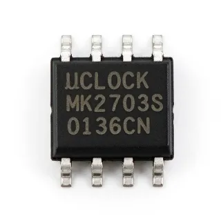
The principal verified characteristics are a maximum clock frequency of 160 MHz, one fanout output, and an 8-SOIC surface-mount package with a stated width of 3.90 mm. The distributor data also classifies ICS571M under Clock Generators, PLLs, and Frequency Synthesizers, reflecting its primary use within clock and timing systems. Detailed supply-voltage, output-impedance, skew, jitter, and temperature limits were not present in the supplied verified records.
ICS571M is suited to communication equipment, processor clock networks, data converters, instrumentation, and industrial electronics requiring local clock distribution. Its small SOIC outline supports compact designs, while the zero-delay architecture can be preferable when an upstream source must drive several clocked loads without intentionally adding another propagation-delay stage.
Designers should verify input slew rate, output loading, supply voltage, and timing margins against the manufacturer datasheet before release. Decoupling and return-path planning remain important because a clock buffer can reproduce upstream supply noise and edge distortion at every distributed output. PCB length matching may also be required in systems with stringent setup-and-hold limits.
This product record consolidates verified distributor specifications, sourcing links, practical application guidance, and honest data-gap disclosures. It also distinguishes confirmed parameters from values that require datasheet review, helping engineers make a technically defensible selection without treating unverified electrical limits as guaranteed specifications.
드롭인 대체품: ICS571M — 동일 패키지, 핀 호환. PCB 재작업이 필요한 다른 패키지 부품은 제외됩니다.
이 제품에는 사용 가능한 드롭인 대체품이 없습니다.
대체품 요청ICS571M 사양
| Product Type | Fanout distribution zero-delay buffer |
| 최대 클록 주파수 | 160 MHz |
| Fanout | 1 output |
| 패키지 | 8-SOIC |
| Package Width | 3.90 mm |
| 실장 유형 | Surface mount |
| 핀 수 | 8 pins |
| Device Class | Clock and timing IC |
| Buffer Type | Zero-delay buffer |
| Distribution Function | Fanout distribution |
ICS571M 3.90 mm 핀 구성 가이드
ICS571M(3.90 mm 패키지)의 핀 구성입니다. 핀 번호, 기능, 연결 다이어그램은 제조사 데이터시트에 정의되어 있습니다. 정확한 풋프린트와 솔더링 지침은 해당 문서를 참조하십시오.

다음에 대한 상세 핀아웃 데이터 없음: ICS571M.
다음을 참조하십시오: 데이터시트 전체 핀 구성은 다음을 참조하십시오.
일반적인 애플리케이션
ICS571M 적합 용도: 6 애플리케이션s: Processor Clock Distribution, Communication Equipment Clocking, Data Converter Clock Input, Industrial Control and Automation, Instrumentation and Test Equipment, Audio and Signal-Conversion Systems.
Processor Clock Distribution
ICS571M can serve as a local zero-delay clock distribution element in systems where a central oscillator or controller must provide a clean edge to another logic block. Its verified 160 MHz rating makes it relevant to processor-adjacent clock networks operating below that frequency, while the 8-SOIC package supports compact layouts. The zero-delay function avoids intentionally adding another conventional buffer delay. Because supply range, jitter, skew, and output-impedance limits are not present in the verified records, the processor timing budget must be checked against the manufacturer datasheet before release.
추천
Communication Equipment Clocking
The ICS571M is applicable within communication equipment that distributes a periodic timing signal to one downstream logic section. Its confirmed 160 MHz maximum frequency covers many interface, control, and data-conversion clock domains, while its fanout-buffer classification supports local distribution. The 8-SOIC package is convenient for legacy and mixed-signal boards that already use that footprint. Engineers must still establish input edge rate, allowable loading, and channel-to-destination timing because those values were not supplied by the verified distributor records.
추천
Data Converter Clock Input
ICS571M can provide a local clock-buffer stage ahead of a converter, digital signal processor, or other timing-sensitive input. The verified zero-delay behavior is useful when adding distribution should not intentionally lengthen the clock path, and the one-output configuration suits designs where only one branch requires buffering. Its 160 MHz class supports high-speed digital processing when all other electrical requirements are satisfied. Confirm output jitter, edge slew, supply range, and the converter's input-current requirements before treating the buffer as a drop-in clock-tree solution.
추천
Industrial Control and Automation
ICS571M can be used in industrial control equipment as a local timing-distribution element between a timing source and a logic or sensing subsystem. Its 8-SOIC package is suitable for conventional surface-mount assemblies, and the verified 160 MHz capability provides substantial margin for slower control and monitoring clocks. Fanout-buffer use can also isolate the source from a specific destination's input loading. Industrial designs should verify operating-temperature limits, supply behavior, and timing tolerances from the manufacturer datasheet because those environmental and electrical details are unavailable in the supplied records.
추천
Instrumentation and Test Equipment
The ICS571M is suitable for instrumentation clock routing where a master timing reference must feed a measurement, control, or conversion subsystem through a compact buffer stage. Its verified 160 MHz maximum frequency accommodates fast digital control paths, while the zero-delay description helps preserve source-to-destination edge timing. The 8-SOIC format simplifies adoption on existing measurement boards. For instrumentation quality, engineers should review jitter, skew, supply sensitivity, and output edge measurements because the verified records do not specify those parameters.
추천
Audio and Signal-Conversion Systems
ICS571M can provide a local clock branch in audio and mixed-signal systems where a converter, digital processor, or control IC requires a separately routed timing edge. The zero-delay fanout function is useful when the architecture includes another distribution point beyond the master clock generator, and the 8-SOIC package keeps the implementation compact. Audio performance is governed by clock jitter and noise coupling in addition to frequency, so the unsupported timing and supply specifications must be verified. PCB return paths and local decoupling should follow the manufacturer's layout guidance.
추천
추천 제품 요약
엔지니어링 참조 데이터: ICS571M — 비교, 설계 지침 및 규정 준수 정보.
선택 가이드
대체품과의 비교
| 파라미터 | 이 제품 |
|---|---|
| Product Type | Fanout distribution zero-delay buffer |
| Maximum Clock Frequency | 160 MHz |
| Fanout | 1 output |
| Package | 8-SOIC |
| Package Width | 3.90 mm |
| Brand | Renesas Electronics |
주요 차별점
- Verified 160 MHz clock-buffer capability (vs ICS574MLF)
- Confirmed 8-SOIC package and body width (vs ICS574MLF)
- Purpose-defined zero-delay distribution (vs General-purpose logic buffer)
설계 노트
Use the manufacturer datasheet pinout before routing the 8-SOIC footprint; the supplied records confirm the package but do not expose pin names. Place the device near the clock source or destination according to the clock architecture, keep the clock trace short, and provide a continuous ground reference. Verify unused-output and exposed-pad requirements instead of assuming standard SOIC conventions.
Validate the complete clock edge at the destination with an oscilloscope rather than relying only on nominal frequency. The verified 160 MHz figure does not specify allowable input slew rate, jitter, skew, or output impedance. Account for trace capacitance, receiver loading, and shared return-path impedance during schematic review, then test the populated board across its expected supply and temperature conditions.
Follow the manufacturer's input and output decoupling recommendations, which were not included in the supplied verified records. Place the specified capacitor adjacent to the relevant supply pin and keep the high-frequency return path compact. If the upstream source is a switching regulator, evaluate clock-edge quality at the buffer input because power-rail ripple can be transferred to every clocked load.
규정 준수 정보
The supplied verified records do not explicitly state RoHS, REACH, AEC-Q100, lead-free, halogen-free, or conflict-minerals status. These fields remain unknown rather than being inferred from the distributor listing.