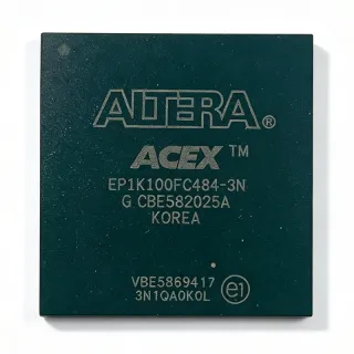
M2GL025T-FG484 - 27.6K Logic Elements Flash FPGA | Microchip
부품 번호: M2GL025T-FG484 ✓ 활성M2GL025T-FG484 개요
An FPGA is a programmable semiconductor whose logic fabric, routing, and I/O blocks can be configured after manufacture. The IGLOO2 family sits within the broader semiconductor hierarchy of configurable logic devices, alongside CPLDs, and is used when designers need more logic capacity or parallel and serial interface flexibility than a conventional microcontroller provides.
The M2GL025T part provides 27,696 logic elements, 267 I/Os, and a 1.2 V core operating voltage. Its flash-based configuration supports reprogrammability without a separate configuration PROM. The IGLOO2 feature set also supports general-purpose networking functions such as Gigabit Ethernet or dual PCI Express control planes, bridging, I/O expansion and conversion, video and image processing, system management, and secure connectivity.
The target MPN is identified as the commercial-temperature version in a 484-ball FBGA package, with an operating range from 0°C to +85°C. The 484-ball package provides a dense, board-routable connection to the programmable fabric and mixed I/O resources, making it appropriate for compact systems requiring substantial parallel I/O alongside programmable serial links.
Typical implementations include industrial Ethernet interfaces, PCI Express endpoint and control-plane logic, protocol bridges, parallel-to-serial converters, machine vision preprocessors, embedded system-management controllers, and secure connectivity modules. The same programmable fabric can support multiple interface personalities, allowing a single board design to adapt as system requirements evolve.
PCB implementation requires careful BGA escape routing, solid power and ground distribution, and decoupling close to the supply pins. Designers should use the IGLOO2 FG484 packaging and pin-description documentation to assign every ball correctly, and should review the high-speed serial constraints before routing high-speed differential pairs.
This page consolidates the verified device identity, package details, interface capabilities, sourcing structure, alternative-device guidance, and practical design considerations into a design-focused reference for engineers evaluating the M2GL025T-FG484.
드롭인 대체품: M2GL025T-FG484 — 동일 패키지, 핀 호환. PCB 재작업이 필요한 다른 패키지 부품은 제외됩니다.
M2GL025-FG484
✅ 드롭인가격 문의
데이터시트 보기 →M2GL025T-1FG484
✅ 드롭인📋 참조 대체품 (카탈로그에 없음)
M2GL025T-FGG484
✅ 드롭인📋 참조 대체품 (카탈로그에 없음)
M2GL025T-FGG484I
✅ 드롭인📋 참조 대체품 (카탈로그에 없음)
M2GL025T-1FGG484I
✅ 드롭인📋 참조 대체품 (카탈로그에 없음)
M2GL025T-FG484 최대 정격 & 전기적 특성
| Device Type | IGLOO2 low-density flash FPGA |
| Logic Elements | 27,696 logic elements |
| Equivalent LUT Capacity | 25K LUTs |
| User I/O Count | 267 I/Os |
| Core Operating Supply Voltage | 1.2 V |
| Configuration Memory | Embedded flash |
| Minimum Operating Temperature | 0°C |
| Maximum Operating Temperature | +85°C |
| 패키지 | 484-ball FBGA |
| Package Designation | FG484 |
| 실장 유형 | SMD/SMT |
| Packaging | Tray |
M2GL025T-FG484 fg484 핀 구성 가이드
M2GL025T-FG484(fg484 패키지)의 핀 구성입니다. 이 디지털 IC에는 GPIO, 통신 인터페이스(UART, SPI, I2C), 전원 핀이 포함되어 있습니다. 대체 핀 기능과 구성 옵션은 제조사 데이터시트를 참조하십시오. 임베디드 시스템 설계와 PCB 레이아웃에 필수적입니다.

다음에 대한 상세 핀아웃 데이터 없음: M2GL025T-FG484.
다음을 참조하십시오: 데이터시트 전체 핀 구성은 다음을 참조하십시오.
일반적인 애플리케이션
M2GL025T-FG484 적합 용도: 6 애플리케이션s: Gigabit Ethernet Interface, PCI Express Control Plane, Protocol Bridge and I/O Conversion, Video and Image Processing, Industrial System Management, USB Connectivity and Embedded Control.
Gigabit Ethernet Interface
The M2GL025T-FG484 is well matched to Gigabit Ethernet interface designs because it combines 27,696 logic elements with 267 user I/Os and programmable high-speed serial resources. A typical implementation can place the Ethernet MAC, packet-processing logic, status and control registers, and board-level interfaces within one low-density IGLOO2 device. The 1.2 V core architecture supports integration of multiple clock domains, while the 267 I/Os provide generous parallel connectivity for PHY control, LEDs, reset sequencing, and diagnostic signals. Engineers should use the M2GL025T data sheets to select legal I/O standards and verify the transceiver lanes required for the chosen Ethernet PHY.
추천
PCI Express Control Plane
The M2GL025T-FG484 supports general-purpose PCI Express control-plane functions by providing programmable logic, serial interfaces, and a high 267-I/O count in a 484-ball FBGA. Control logic, endpoint functions, arbitration, status reporting, and system-management functions can be consolidated without relying on a large processor for protocol implementation. The M2GL025 family is specifically identified for dual PCI Express control-plane applications, although the final lane count and endpoint arrangement must be confirmed for the exact device configuration. Clocking, reference voltage, transmitter equalization, and impedance-controlled routing should be reviewed against the manufacturer’s high-speed design guidance.
추천
Protocol Bridge and I/O Conversion
The M2GL025T-FG484 is useful for bridging legacy parallel buses to modern serial links because its 27,696 logic elements can implement state machines, buffering, command translation, and timing isolation. Its 267 I/Os accommodate the parallel side of the bridge as well as control, interrupt, and configuration signals, while programmable serial interfaces handle the high-speed side. This implementation approach can consolidate two or more discrete interface controllers into a compact programmable block. Engineers should establish maximum clock rates, protocol timing margins, and I/O direction constraints in the HDL before selecting the final device speed grade and committing the PCB footprint.
추천
Video and Image Processing
The M2GL025T-FG484 can implement preprocessing functions in compact video and image-processing systems, including pixel routing, thresholding, frame timing, color-channel coordination, and sensor-interface control. Its 27,696 logic elements and 267 I/Os provide enough parallelism to combine programmable data paths with acquisition and display-control signals. The flash-based IGLOO2 architecture also permits field updates when algorithms or board behavior need to change. For production designs, constrain external memory or image-sensor timing, verify the selected I/O voltage standards, and use timing analysis to separate pixel-clock, control, and serial-data paths.
추천
Industrial System Management
The M2GL025T-FG484 fits industrial system-management and secure-connectivity roles where monitoring, sequencing, diagnostics, and programmable I/O are needed in a compact controller. The 0°C to +85°C operating range covers many indoor and enclosure-controlled industrial environments, while the embedded flash configuration supports field-programmable behavior. Designers can assign health monitoring, alarm handling, watchdog logic, bus arbitration, and secure-access control functions to the fabric and use the 267 I/Os for sensors, relays, and communication links. Production qualification should separately evaluate electromagnetic compatibility, surge immunity, temperature extremes, and functional-safety requirements.
추천
USB Connectivity and Embedded Control
The M2GL025T-FG484 can serve as a programmable USB interface or embedded control element when a design needs flexible endpoint behavior, protocol monitoring, or low-latency data routing. Its programmable logic fabric is suited to implementing device-specific packet handling and control logic, while 267 I/Os support USB control lines, sideband signals, status LEDs, and auxiliary interfaces. The integrated flash configuration permits product revisions without a separate configuration device. Designers must confirm the exact USB controller resources in the M2GL025T device configuration and follow the manufacturer’s constraints for high-speed differential routing, reference voltage, and power sequencing.
추천
추천 제품 요약
엔지니어링 참조 데이터: M2GL025T-FG484 — 비교, 설계 지침 및 규정 준수 정보.
선택 가이드
대체품과의 비교
| 파라미터 | 이 제품 | M2GL025-FG484 | M2GL025T-1FG484 | M2GL025T-FGG484 | M2GL025T-FGG484I | M2GL025T-1FGG484I |
|---|---|---|---|---|---|---|
| Brand | Microchip Technology | Microchip Technology | Microchip Technology | Microchip Technology | Microchip Technology | Microchip Technology |
| Package | 484-ball FBGA (FG484) | 484-ball FBGA - same | 484-ball FBGA - same | 484-ball FBGA - same | 484-ball FBGA - same | 484-ball FBGA - same |
| FPGA Family | IGLOO2 | IGLOO2 | IGLOO2 | IGLOO2 | IGLOO2 | IGLOO2 |
| Ordering Suffix | M2GL025T-FG484 | M2GL025-FG484 - T suffix omitted | M2GL025T-1FG484 - -1 suffix added | M2GL025T-FGG484 - FGG suffix | M2GL025T-FGG484I - FGG and I suffixes | M2GL025T-1FGG484I - -1, FGG, and I suffixes |
주요 차별점
- Consistent logic and I/O density across the M2GL025 family (vs M2GL025-FG484)
- Direct FG484 migration path within the same device family (vs M2GL025T-1FG484)
- One-device consolidation for dense parallel and serial interfaces (vs M2GL025-FG484)
- Broad design reuse across multiple IGLOO2 ordering options (vs M2GL025T-FGG484)
설계 노트
Use Microchip’s IGLOO2 Packaging and Pin Descriptions User Guide for the FG484 land pattern, ball map, bank assignments, and power requirements. Route the 484-ball BGA with a manufacturing process capable of the required ball pitch and via-in-pad or microvia rules. Keep power and ground planes continuous beneath the device, and place bypass capacitors close to the relevant supply balls so switching and high-speed outputs cannot pull the core rail outside its permitted operating range.
Separate high-speed serial pairs from clocks and sensitive control inputs, use symmetric routing for differential pairs, and maintain the manufacturer-referenced impedance and spacing values. The M2GL025 family supports high-speed serial features, but their performance depends on clean reference voltages and controlled launch geometry. Avoid routing clocks parallel to long serial runs and minimize stubs so switching noise and reflection do not compromise interface margins.
Do not treat a shared 484-ball package name as proof that every FG484 ordering suffix is interchangeable. Before substituting M2GL025-FG484, M2GL025T-1FG484, or an FGG484 variant, compare speed grade, temperature range, qualification status, and acquisition qualification in the manufacturer ordering guide. Review Microchip application note AC402 for migration guidance, then rerun timing analysis and verify that the configuration bitstream remains valid for the selected ordering configuration.
Plan the 1.2 V core supply as a dedicated, low-impedance rail and determine external I/O voltage requirements separately from the core voltage. Check the device’s power-up and power-down sequencing requirements in the manufacturer documentation. Use local bulk and high-frequency bypass capacitance, provide adequate source current for simultaneous I/O activity, and avoid relying on general-purpose board supply routing for the most sensitive logic and serial-reference connections.
규정 준수 정보
No specific compliance declarations are stated for the exact M2GL025T-FG484 ordering suffix. Confirm RoHS, REACH, lead-free, halogen-free, conflict-minerals, and automotive qualification status against the manufacturer’s current product documentation before release.