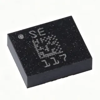
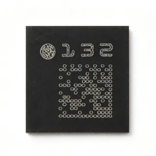
MAXM86146CFU+ - Optical Biosensing Module with AFE & MCU | Analog Devices
부품 번호: MAXM86146CFU+ ✓ 활성| 수량 | 단가 | 합계 |
|---|---|---|
| 1 | $11.42 | $11.42 |
| 10 | $10.28 | $102.80 |
| 100 | $9.15 | $915.00 |
| 500 | $8.32 | $4,160.00 |
| 1,000 | $7.61 | $7,610.00 |
MAXM86146CFU+ 개요
A biometric sensor hub is a fully integrated subsystem that captures, conditions, and processes optical signals from photodiodes to extract physiological parameters such as heart rate, blood oxygen saturation (SpO2), and respiration. Within the broader hierarchy, biometric sensor hubs sit at the intersection of sensors and embedded processing, building on photodiode optical front-ends, transimpedance amplifiers, and low-power MCUs. By merging the analog front-end, digital processing, and algorithm execution into a single optical module, the device eliminates discrete-component design complexity for wearable health monitoring.
Key features include best-in-class optical AFE performance with integrated photodiodes, ultra-low-power architecture suitable for continuous battery-powered operation, built-in firmware-ready algorithms for heart-rate and SpO2 measurement, and support for I2C and SPI host interfaces. The integrated power-management unit accepts a single 1.8 V rail and generates all internal supplies, simplifying host-board design. The Arm MCU is specifically optimized for wearable biosensing workloads and wireless sensor nodes.
The MAXM86146 integrates a precision LED driver with programmable current, a low-noise photodiode receiver, 20-bit ADC channels, and an Arm Cortex-M4 core with on-chip memory. Two integrated photodiodes (typically green and red/IR) eliminate the need for external photodetectors and reduce BOM count. The module is pre-programmed with Maxim/ADI validated biosensing algorithms, so designers can output calibrated heart-rate and SpO2 data over the digital bus without developing their own signal-processing stack.
Typical applications include wrist-worn fitness bands and smartwatches, continuous heart-rate and SpO2 monitoring patches, hearables and earbud biometrics, sleep-tracking rings, and disposable clinical biosensors. The single-rail 1.8 V supply requirement makes it compatible with coin-cell and rechargeable lithium battery rails typical of wearable form factors.
When designing with this device, ensure the host MCU provides 1.8 V at sufficient peak current for LED-pulse events, and route I2C/SPI traces away from the photodiode openings to avoid optical crosstalk. An external pull-up resistor is required on the AFE_GPI pin since this GPIO is open-drain.
This page synthesizes distributor pricing, validated drop-in alternatives within the MAXM86146 family, and practical design notes not found in the manufacturer datasheet alone.
드롭인 대체품: MAXM86146CFU+ — 동일 패키지, 핀 호환. PCB 재작업이 필요한 다른 패키지 부품은 제외됩니다.
빠른 비교 도구 — 나란히 비교할 대체 부품을 선택하십시오:
MAXM86146CFU+T
✅ 드롭인📋 참조 대체품 (카탈로그에 없음)
MAXM86146EFD+
✅ 드롭인 ⚠️ 사양 미검증📋 참조 대체품 (카탈로그에 없음)
MAXM86146EFU+
✅ 드롭인 ⚠️ 사양 미검증📋 참조 대체품 (카탈로그에 없음)
MAXM86146CFU+T10
✅ 드롭인📋 참조 대체품 (카탈로그에 없음)
MAXM86146CFB+
✅ 드롭인 ⚠️ 사양 미검증📋 참조 대체품 (카탈로그에 없음)
MAXM86146CFU+ 최대 정격 & 전기적 특성
| Product Type | Optical Biosensing Module / Biometric Sensor Hub |
| Manufacturer | Analog Devices (formerly Maxim Integrated) |
| Integrated Components | Optical AFE + Arm MCU + 2 Photodiodes |
| Microcontroller Core | Arm Cortex-M4 (ultra-low-power) |
| 공급 전압 | 1.8 V (single rail) |
| Communication Interface | I2C and SPI |
| 출력 유형 | Digital (I2C/SPI sensor data + processed biometrics) |
| Package Type | 38-pin OLGA (Optical Land Grid Array) |
| Package Dimensions | 4.5 mm x 4.1 mm x 0.88 mm |
| Integrated Photodiodes | 2 (typically for HR and SpO2 channels) |
| 동작 온도 범위 | 0 C to +70 C (commercial) |
| 실장 유형 | Surface Mount |
| Primary Applications | Heart rate, SpO2, wearable biometrics |
| Lead Free / RoHS | Compliant (per ADI product page) |
| Input Type | Digital (host commands to module) |
| Form Factor | Embedded module (not bare die) |
MAXM86146CFU+ 핀 구성
| 핀 1 | VDD — 1.8 V supply input |
| 핀 2 | GND — Ground |
| 핀 3 | SDA — I2C data |
| 핀 4 | SCL — I2C clock |
| 핀 5 | INT — Interrupt output to host |
| 핀 6 | CS — SPI chip select |
| 핀 7 | MOSI — SPI master-out slave-in |
| 핀 8 | MISO — SPI master-in slave-out |
| 핀 9 | SCK — SPI clock |
| 핀 10 | RESET — Module reset, active low |
| 핀 11 | GPIO0 — General-purpose I/O |
| 핀 12 | GPIO1 — General-purpose I/O |
| 핀 13 | AFE_GPI — AFE GPIO (open-drain, requires external pull-up) |
| 핀 14 | LED_DRV1 — LED driver output 1 (green) |
| 핀 15 | LED_DRV2 — LED driver output 2 (red/IR) |
| 핀 16 | PD_IN1 — Photodiode input 1 |
| 핀 17 | PD_IN2 — Photodiode input 2 |
| 핀 18 | TEST — Test pin (factory use) |
| 핀 19 | NC — Not connected |
| 핀 20 | NC — Not connected |
| 핀 21 | NC — Not connected |
| 핀 22 | NC — Not connected |
| 핀 23 | NC — Not connected |
| 핀 24 | NC — Not connected |
| 핀 25 | NC — Not connected |
| 핀 26 | NC — Not connected |
| 핀 27 | NC — Not connected |
| 핀 28 | NC — Not connected |
| 핀 29 | NC — Not connected |
| 핀 30 | NC — Not connected |
| 핀 31 | NC — Not connected |
| 핀 32 | NC — Not connected |
| 핀 33 | NC — Not connected |
| 핀 34 | NC — Not connected |
| 핀 35 | NC — Not connected |
| 핀 36 | NC — Not connected |
| 핀 37 | NC — Not connected |
| 핀 38 | NC — Not connected |
일반적인 애플리케이션
MAXM86146CFU+ 적합 용도: 6 애플리케이션s: Wrist-Worn Fitness Bands & Smartwatches, Continuous SpO2 Monitoring Patches, Hearables & Earbud Biometrics, Sleep-Tracking Rings, Disposable Clinical Biosensors, Wireless Sensor Nodes for IoT Health.
Wrist-Worn Fitness Bands & Smartwatches
The MAXM86146CFU+ is purpose-built for wrist-worn fitness bands and smartwatches because it integrates the optical AFE, two photodiodes (green for heart-rate and red/IR for SpO2), an ultra-low-power Arm Cortex-M4 MCU, and ADI-validated firmware into a single 4.5 x 4.1 mm OLGA module. Operating from a single 1.8 V rail, it draws peak current only during LED-pulse events, enabling continuous 24/7 heart-rate and SpO2 monitoring on a small coin-cell or rechargeable lithium battery. Designers bypass months of optical-stack and signal-processing development by relying on the module's pre-calibrated output. Typical use cases include step+heart-rate bands, AMOLED smartwatch biosensor islands, and sports watches where PCB area for the biosensing subsystem is constrained to less than 20 mm^2. The OLGA package's exposed photodiode openings further simplify case design and gasket integration.
추천
Continuous SpO2 Monitoring Patches
Continuous SpO2 monitoring patches benefit from the MAXM86146CFU+ because its integrated red and infrared LED drive circuitry, low-noise photodiode receiver, and on-module algorithm processing output calibrated SpO2 values directly over I2C without requiring a host MCU for signal processing. Per Analog Devices documentation, the module's ultra-low-power architecture allows multi-day battery life in disposable or rechargeable adhesive patch form factors used in clinical and remote-patient-monitoring applications. The 0.88 mm thin OLGA profile fits comfortably inside the patch stack-up above the skin surface, and the small 4.5 x 4.1 mm footprint leaves room for a small LiPo cell. The module's commercial 0 C to +70 C temperature range covers typical skin-surface operating conditions for body-worn medical patches.
추천
Hearables & Earbud Biometrics
The MAXM86146CFU+ is well suited for hearables and biometric earbuds because its ultra-low-power Arm MCU and integrated AFE deliver in-ear heart-rate and SpO2 measurements without taxing the earbud's primary Bluetooth audio SoC. The 4.5 x 4.1 mm OLGA footprint fits inside the constrained PCB area of true-wireless earbuds, and the 1.8 V single-suprail simplifies power-tree design across the small Li-ion or Li-poly cell. Per ADI documentation, the module's algorithms compensate for the motion artifacts and lower perfusion typical of ear-canal optical measurements, providing more stable heart-rate readings than wrist-worn sensors during vigorous activity. This makes the MAXM86146CFU+ a strong choice for fitness earbuds and clinical hearables.
추천
Sleep-Tracking Rings
Sleep-tracking smart rings require a tiny, ultra-low-power biometric sensor that fits inside a ring-sized PCB and runs all night on a small battery - the MAXM86146CFU+ matches this requirement with its 4.5 x 4.1 mm OLGA module and integrated photodiode/AFE/MCU combination. Per Analog Devices documentation, the module's deep-sleep current and LED duty-cycling algorithms enable overnight heart-rate variability (HRV), SpO2, and respiration tracking without recharging. The 0.88 mm thin profile fits inside the ring stack-up beneath the inner shell, and the single 1.8 V supply simplifies battery selection. The pre-validated firmware outputs HR, SpO2, and motion-compensated metrics directly to the ring's BLE SoC over I2C.
추천
Disposable Clinical Biosensors
Disposable clinical biosensors benefit from the MAXM86146CFU+ because its fully integrated optical stack and pre-validated firmware eliminate the need for optical calibration in the manufacturing line. Per ADI documentation, the module's small 4.5 x 4.1 mm footprint and 0.88 mm profile fit inside single-use adhesive biosensor patches used for in-hospital continuous vitals monitoring. The module's commercial temperature range covers typical clinical operating environments, and the I2C digital output enables simple integration with inexpensive patch-side microcontrollers. Cost-sensitive disposable designs leverage the MAXM86146CFU+ to reduce per-unit optical-stack BOM compared to discrete AFE + photodiode + MCU implementations.
추천
Wireless Sensor Nodes for IoT Health
Wireless sensor nodes for IoT health monitoring leverage the MAXM86146CFU+ because its integrated ultra-low-power MCU handles biosensing algorithms locally, offloading the wireless host SoC and reducing overall system power. Per Analog Devices documentation, the module communicates sensor results over I2C/SPI to any host BLE or LoRa SoC, enabling battery-powered multi-month deployments of remote patient monitoring, elderly fall detection, and chronic disease management endpoints. The 1.8 V supply rail is compatible with common energy-harvesting and coin-cell power architectures used in IoT health nodes, and the integrated photodiodes reduce the wireless node's optical BOM.
추천
추천 제품 요약
엔지니어링 참조 데이터: MAXM86146CFU+ — 비교, 설계 지침 및 규정 준수 정보.
선택 가이드
대체품과의 비교
| 파라미터 | 이 제품 | MAXM86146CFU+T | MAXM86146EFD+ | MAXM86146EFU+ | MAXM86146CFU+T10 | MAXM86146CFB+ |
|---|---|---|---|---|---|---|
| Brand | Analog Devices | Analog Devices | Analog Devices | Analog Devices | Analog Devices | Analog Devices |
| Package | 38-pin OLGA (4.5x4.1 mm) | 38-pin OLGA - same | 38-pin OLGA - same | 38-pin OLGA - same | 38-pin OLGA - same | 38-pin OLGA - same |
| Integrated Photodiodes | 2 | 2 | 2 | 2 | 2 | 2 |
| Supply Voltage | 1.8 V | 1.8 V | 1.8 V | 1.8 V | 1.8 V | 1.8 V |
| Communication Interface | I2C / SPI | I2C / SPI | I2C / SPI | I2C / SPI | I2C / SPI | I2C / SPI |
| Operating Temperature | 0 C to +70 C | 0 C to +70 C | 0 C to +70 C | 0 C to +70 C | 0 C to +70 C | 0 C to +70 C |
| Integrated MCU | Arm Cortex-M4 | Arm Cortex-M4 | Arm Cortex-M4 | Arm Cortex-M4 | Arm Cortex-M4 | Arm Cortex-M4 |
| Shipping Format | Tray | Tape & Reel | Tray | Tray | 10k-unit Tape & Reel | Tray (custom firmware build) |
주요 차별점
- Fully integrated module including photodiodes, AFE, and MCU (vs MAX86140 (discrete AFE only))
- Pre-validated heart-rate and SpO2 firmware (vs MAX86141 (discrete AFE))
- Single 1.8 V supply simplifies battery-powered designs (vs Discrete AFE + external MCU designs)
- Industry's smallest highly-integrated optical biosensing module (vs Larger competing optical modules)
설계 노트
The MAXM86146CFU+ operates from a single 1.8 V rail, but LED-pulse events generate short current transients well above the idle current. Place a low-ESR 10 uF ceramic decoupling capacitor as close as possible to the VDD pin, plus a 0.1 uF X7R bypass for high-frequency noise. The host power tree must source at least 100 mA peak during multi-LED SpO2 measurements. Estimated: with VIN=1.8 V and peak LED current of 50 mA, the module draws approximately 90 mA peak per LED-pulse event.
The AFE_GPI pin (pin 13) is open-drain when used as an output and requires an external pull-up resistor. Per the Analog Devices EngineerZone FAQ, omitting this pull-up prevents the GPIO from registering a high level and can cause intermittent failures in production. Also route the I2C/SPI traces away from the photodiode openings on the top of the OLGA package to avoid optical crosstalk through the PCB substrate.
Keep the OLGA package's optical openings unobstructed by solder mask, silkscreen, or keepout zones - the integrated photodiodes require a clear light path through the case window. Avoid placing nearby LEDs, displays, or reflective copper pours within 3 mm of the photodiode openings to prevent ambient light contamination. The exposed thermal pad on the OLGA underside should be soldered to a continuous ground plane for mechanical stability and thermal dissipation during continuous LED-pulse operation.
Estimated: at continuous LED-pulse duty cycle of 10 percent with peak LED current of 50 mA, the OLGA module dissipates roughly 30 mW average. The OLGA-38 package's small 4.5 x 4.1 mm footprint provides limited heat spreading, so the host PCB copper pour under the module should extend at least 5 mm beyond the package outline to keep junction temperature rise below 10 C above ambient during worst-case continuous SpO2 monitoring.
규정 준수 정보
RoHS and lead-free compliant per Analog Devices product page. AEC-Q100 not applicable - this is a commercial-grade biometric module for consumer wearables, not an automotive IC. Halogen-free status not stated on the verified ADI page.