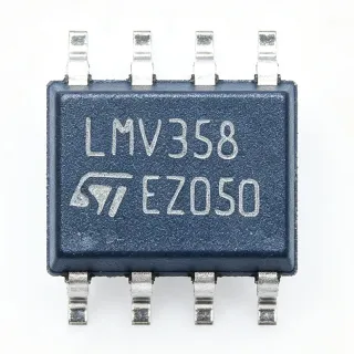
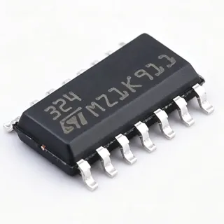
MC34184M - Low-Power Quad JFET Op Amp | onsemi
부품 번호: MC34184M ✗ 단종MC34184M 개요
A JFET-input operational amplifier is a voltage-amplifier device whose input stage uses junction field-effect transistors. This input architecture provides high input resistance and low input bias current while supporting relatively low supply-current operation. Within the power-management and analog-signal hierarchy, the MC34184M belongs to the operational-amplifier family and functions as a high-impedance buffer or closed-loop gain stage between sensors, transducers, analog switches, and downstream conversion or control circuitry.
The primary performance characteristics of the MC34184M include a 4.0 MHz gain-bandwidth product, 10 V/us slew rate, and approximately 210 uA of supply current per amplifier. Its JFET input stage provides high input resistance, low input offset voltage, and high open-loop gain according to the Motorola MC34184 datasheet. These characteristics make the amplifier appropriate for precision current-voltage conversion, low-level signal amplification, active filtering, and feedback networks operating at low or moderate frequencies.
The family architecture also supports practical instrumentation requirements because low input bias current reduces disturbance of high-impedance sources. A high gain-bandwidth product allows useful closed-loop bandwidth above the audio range when configured with conventional compensation and suitable external resistors. The 10 V/us slew rate improves handling of moderately fast signal edges, although the 4.0 MHz bandwidth places the device in the general-purpose precision-amplifier class rather than the high-speed operational-amplifier class.
Typical applications include bridge-sensor signal conditioning, biomedical instrumentation, photodiode and phototransistor amplifiers, audio preamplification, active filters, sample-and-hold stages, and low-frequency closed-loop control loops. In each case, the amplifier should be evaluated for input common-mode range, output swing, noise, offset, stability, and supply compatibility under the actual operating conditions.
Designers should verify the package dimensions, pin numbering, electrical limits, and common-mode range against the manufacturer documentation before layout. Input and feedback resistors must also be selected for low thermal noise and acceptable bias-current error. Bias compensation may be useful when source resistance is high enough that input bias current produces a material offset across the source impedance.
This page organizes the core MC34184M electrical characteristics, practical application guidance, comparison parameters, and design considerations into one engineering-focused reference. It supports early architecture selection while preserving the need to verify production details, lifecycle commitments, and assembly-specific information with the manufacturer before releasing a design.
드롭인 대체품: MC34184M — 동일 패키지, 핀 호환. PCB 재작업이 필요한 다른 패키지 부품은 제외됩니다.
이 제품에는 사용 가능한 드롭인 대체품이 없습니다.
대체품 요청MC34184M 최대 정격 & 전기적 특성
| Amplifier Type | Quad JFET-input operational amplifier |
| Supply Current per Amplifier | 210 uA |
| Gain-Bandwidth Product | 4.0 MHz |
| Slew Rate | 10 V/us |
| Input Stage Architecture | JFET input |
MC34184M standard 핀 구성 가이드
MC34184M(standard 패키지)의 핀 구성입니다. 이 아날로그 부품에는 입력, 출력, 전원 공급 핀이 있습니다. 오프셋 널, 보상, 인에이블 핀 구성은 제조사 데이터시트를 참조하십시오. 신호 컨디셔닝 및 증폭기 회로에 이상적입니다.

다음에 대한 상세 핀아웃 데이터 없음: MC34184M.
다음을 참조하십시오: 데이터시트 전체 핀 구성은 다음을 참조하십시오.
일반적인 애플리케이션
MC34184M 적합 용도: 6 애플리케이션s: High-Impedance Sensor Signal Conditioning, Precision Bridge Measurement, Active Audio Filter, Photodiode and Optical Sensor Interface, Low-Frequency Control Loop, Sample-and-Hold Signal Path.
High-Impedance Sensor Signal Conditioning
The MC34184M fits low-level sensor amplification because its JFET input stage provides high input resistance and low input bias current, while the 4.0 MHz gain-bandwidth product supports moderate closed-loop bandwidth. Use one channel as a transimpedance or voltage amplifier ahead of an ADC or data converter. Source resistance, input capacitance, bias-current offset, common-mode range, and output swing must be checked together because a high-impedance sensor can make leakage and stray capacitance more important than raw bandwidth.
Precision Bridge Measurement
A Wheatstone bridge can use two MC34184M channels to amplify the differential bridge error and two additional channels for reference or auxiliary functions. The JFET inputs reduce loading of the bridge, and the 210 uA per-amplifier supply current supports low-power measurement systems. Practical designs should evaluate bridge excitation voltage, common-mode limits, input offset, resistor matching, and the amplifier's ability to preserve low-level signals without saturating during bridge startup or fault conditions.
Active Audio Filter
The MC34184M is appropriate for active audio filtering when a four-channel package simplifies preamplifier and equalizer layouts. Its 4.0 MHz gain-bandwidth product exceeds typical audio-band requirements, and the 10 V/us slew rate supports moderate waveform slopes. Select resistor and capacitor values using the manufacturer's recommended noise-gain relationships, then verify closed-loop stability across the intended frequency range. Output loading, headroom, distortion, and the interaction between adjacent filter channels also influence the final design.
Photodiode and Optical Sensor Interface
For photodiode and optical-sensor interfaces, the MC34184M's low-bias-current JFET input stage helps preserve weak current signals, while its moderate 4.0 MHz bandwidth is useful for low-to-medium-frequency transimpedance loops. The required feedback resistor and compensation capacitor depend on sensor capacitance, and the complete loop must be checked for stability. Input protection, dark-current behavior, temperature drift, and output saturation during high-light conditions are equally important to signal-chain performance.
Low-Frequency Control Loop
The MC34184M can amplify error signals and drive feedback networks in low-frequency control or monitoring loops. Its high open-loop gain supports precise closed-loop behavior, while the 4.0 MHz gain-bandwidth product offers more bandwidth than many slow sensor-control systems require. Verify output current and swing against the actuator or feedback network, include suitable compensation for the plant, and keep sensitive error traces away from switching regulators and digital return currents.
Sample-and-Hold Signal Path
The four channels in the MC34184M can support buffering, gain adjustment, and isolation stages around sample-and-hold systems. The JFET input stage is advantageous when the source presents high impedance, and the 10 V/us slew rate helps preserve moderate transitions after acquisition. Real implementations must account for capacitor leakage, switch charge injection, hold droop, amplifier bias-current error, and settling behavior. The amplifier should also remain within its input and output common-mode limits during every acquisition and hold interval.
엔지니어링 참조 데이터: MC34184M — 비교, 설계 지침 및 규정 준수 정보.
선택 가이드
대체품과의 비교
| 파라미터 | 이 제품 |
|---|---|
| Brand | onsemi |
| Amplifier Count | 4 amplifiers |
| Input Stage | JFET input |
| Supply Current per Amplifier | 210 uA |
| Gain-Bandwidth Product | 4.0 MHz |
| Slew Rate | 10 V/us |
주요 차별점
- Four amplifiers share one package (vs MC34182)
- Low-power JFET input architecture (vs MC34184D)
- Moderate bandwidth with high slew rate (vs MC34182)
설계 노트
Keep the four amplifier input nodes short and isolated from switching nodes. High-impedance inputs can couple leakage and stray capacitance even when the amplifier itself operates below 4.0 MHz. Route sensitive inputs away from inductors, switching-regulator power paths, and exposed connector fields; use a surrounding ground or guard structure where the circuit and manufacturing process permit it.
Do not assume that low input bias current eliminates gain error in every source configuration. Calculate the offset contribution produced by input bias current across the effective source resistance, especially for resistive dividers and sensor outputs. If that error is material, consider bias-current compensation or a lower-offset alternative while also checking temperature drift and the amplifier's input common-mode range.
Verify closed-loop stability at every intended gain rather than relying only on the 4.0 MHz gain-bandwidth-product figure. Include the source capacitance, load capacitance, external resistance, and feedback-network values in the analysis. In photodiode and high-impedance sensor circuits, the feedback capacitor and board parasitics materially shape stability and usable bandwidth.
Bypass the supply pins with a short, low-inductance path and place the capacitor close to the device. The 210 uA per-amplifier rating describes amplifier bias consumption, but total system current also includes output load current, reference circuitry, and switching losses. Confirm the absolute maximum and recommended supply limits from the manufacturer documentation before selecting the system supply.
규정 준수 정보
The technical source does not state the MC34184M compliance declarations, so each status remains unknown.