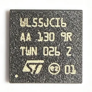
NRF51822-QFAC - BLE/ANT SoC 256kB Flash 48-QFN | Nordic
부품 번호: NRF51822-QFAC ✗ 단종| 수량 | 단가 | 합계 |
|---|---|---|
| 1 | $5.42 | $5.42 |
| 10 | $4.85 | $48.50 |
| 100 | $4.21 | $421.00 |
| 500 | $3.68 | $1,840.00 |
| 1,000 | $3.15 | $3,150.00 |
NRF51822-QFAC 개요
A Bluetooth Low Energy SoC is an integrated circuit that combines a microcontroller, memory, peripherals, and a 2.4 GHz radio in a single die. Within the taxonomy: BLE SoC -> wireless SoC -> microcontroller + transceiver -> semiconductor. BLE SoCs target ultra-low-power connected applications (wearables, beacons, sensors) where discrete MCU + external radio solutions would consume too much board area and power. The NRF51822 family was Nordic's first-generation nRF51 series BLE platform, widely adopted in 2014-2019 designs.
Key features: ARM Cortex-M0 core up to 16 MHz, 256 kB flash for application code, 32 kB RAM, integrated 2.4 GHz radio with -93 dBm RX sensitivity in BLE mode and +4 dBm TX output power, 12-bit/10-bit ADC, 31 GPIO, hardware crypto accelerator (AES), and a flexible PPI (Programmable Peripheral Interconnect) block. The integrated DC-DC converter inductor allows the chip to operate from 1.8 V to 3.6 V supply with peak RX/TX currents around 5-10 mA and sub-uA sleep currents.
Architecturally, the NRF51822 pairs a Cortex-M0 core with a separate 2.4 GHz radio front-end; the radio is driven by Nordic's SoftDevice stack (S110/S120/S130) flashed on top of user application code. This separation isolates protocol updates from application firmware and has driven broad ecosystem support (nRF5 SDK, nRF Connect SDK legacy compatibility, third-party Zephyr and Mynewt ports).
Typical applications include BLE-enabled wearables, fitness/heart-rate sensors, smart-home beacons and sensors, ANT+ sports/fitness devices, industrial wireless sensor nodes, and Apple iBeacon/Eddystone proximity tags. The QFAC variant (256 kB flash / 32 kB RAM) is the highest-memory SKU in the nRF51 family, suitable for applications requiring Over-The-Air (OTA) DFU bootloaders plus application code.
When designing with NRF51822-QFAC, ensure proper RF layout (controlled-impedance antenna trace, pi-matching network, ground plane), supply decoupling (1 uF + 100 nF + 10 nF) and provision a 32.768 kHz crystal if low-power sleep timing is required. For new designs, evaluate the nRF52832 or nRF52840 which add Bluetooth 5, Cortex-M4F, and improved radio sensitivity; the QFAC is recommended only for legacy maintenance or cost-sensitive carry-over designs.
드롭인 대체품: NRF51822-QFAC — 동일 패키지, 핀 호환. PCB 재작업이 필요한 다른 패키지 부품은 제외됩니다.
빠른 비교 도구 — 나란히 비교할 대체 부품을 선택하십시오:
NRF51822-QFAC-R
✅ 드롭인📋 참조 대체품 (카탈로그에 없음)
NRF51822-QFAC-T
✅ 드롭인📋 참조 대체품 (카탈로그에 없음)
NRF51822-QFAA-R
✅ 드롭인📋 참조 대체품 (카탈로그에 없음)
NRF51822-QFAB-R
✅ 드롭인📋 참조 대체품 (카탈로그에 없음)
NRF51422-QFAC-R
✅ 드롭인📋 참조 대체품 (카탈로그에 없음)
NRF52810-QFAA-R
✅ 드롭인📋 참조 대체품 (카탈로그에 없음)
NRF51822-QFAC 최대 정격 & 전기적 특성
| Product Type | Bluetooth Low Energy / 2.4 GHz SoC |
| Core Architecture | ARM Cortex-M0, 32-bit |
| Maximum CPU Clock | 16 MHz |
| Program Memory (Flash) | 256 kB |
| Data Memory (RAM) | 32 kB |
| Radio Frequency | 2.4 GHz ISM band (2400-2483.5 MHz) |
| Wireless Protocol | Bluetooth v4.0 (BLE), ANT, proprietary 2.4 GHz |
| RX Sensitivity (BLE, 1 Mbps) | -93 dBm |
| TX Output Power | +4 dBm maximum |
| Supply Voltage Range | 1.8 V to 3.6 V |
| GPIO Count | 31 |
| ADC | 10/12-bit, 8 channels |
| 패키지 | 48-pin QFN (6x6 mm) with exposed pad |
| 동작 온도 | -40C to +85C |
| RoHS 상태 | Compliant |
NRF51822-QFAC 48-pin qfn (6x6 mm) with exposed pad 핀 구성 가이드
NRF51822-QFAC(48-pin qfn (6x6 mm) with exposed pad 패키지)의 핀 구성입니다. 이 디지털 IC에는 GPIO, 통신 인터페이스(UART, SPI, I2C), 전원 핀이 포함되어 있습니다. 대체 핀 기능과 구성 옵션은 제조사 데이터시트를 참조하십시오. 임베디드 시스템 설계와 PCB 레이아웃에 필수적입니다.

다음에 대한 상세 핀아웃 데이터 없음: NRF51822-QFAC.
다음을 참조하십시오: 데이터시트 전체 핀 구성은 다음을 참조하십시오.
일반적인 애플리케이션
NRF51822-QFAC 적합 용도: 7 애플리케이션s: BLE Wearable Heart-Rate Sensor, iBeacon / Eddystone Proximity Beacon, ANT+ Sports/Fitness Sensor, Wireless Industrial Sensor Node (Modbus-over-BLE), Smart-Home BLE Light Controller, BLE HID / Wireless Keyboard/Mouse Dongle, Medical BLE Pulse Oximeter (Class II).
BLE Wearable Heart-Rate Sensor
Why NRF51822-QFAC fits: the 32 kB RAM holds the BLE GATT service table, the sensor fusion buffer, and the display driver frame buffer simultaneously. The 256 kB flash accommodates the S130 softdevice (~80 kB) plus the heart-rate service, SpO2 algorithm, and OTA-DFU bootloader, leaving headroom for application code. With 31 GPIO the chip directly drives an optical PPG sensor (LED + photodiode front-end), a small OLED, and a single-button UI without external mux ICs. The -93 dBm RX sensitivity provides a robust link to a paired smartphone in a gym environment with body shadowing. The 2.4 GHz radio integrates the balun so the PCB only needs a pi-matching network and a chip antenna.
추천
iBeacon / Eddystone Proximity Beacon
Why NRF51822-QFAC fits: the chip advertises BLE non-connectable beacon frames continuously, and the S130 softdevice handles the radio automatically, leaving the Cortex-M0 free to set TX power and advertising interval. The 2.4 GHz radio can be configured from -20 dBm to +4 dBm in 4 dB steps, which lets designers trade battery life for range. The 31 GPIO can be repurposed to drive a small indicator LED or to read a coin-cell voltage divider. With 1.9 uA sleep current and a 240 mAh CR2032, the device can run over 12 months in 100 ms-interval beacon mode. The exposed-pad QFN provides a low-thermal-resistance package for the 10 mA peak TX current.
추천
ANT+ Sports/Fitness Sensor
Why NRF51822-QFAC fits: with the S310 or S312 softdevice, the NRF51822 supports ANT/ANT+ protocol stack in parallel with BLE, enabling dual-mode operation for heart-rate, speed/cadence, and power-meter ANT+ profiles. The 256 kB flash is sufficient for ANT+ device profiles plus BLE services. The Cortex-M0 runs the sensor sampling at up to 16 MHz while the radio offloads timing-critical ANT channel hopping to hardware. The 32 kB RAM fits the ANT message buffer plus sensor data. Pin compatibility with the NRF51422 family makes it easy to design one PCB that ships in either ANT-only or dual-mode variants.
추천
Wireless Industrial Sensor Node (Modbus-over-BLE)
Why NRF51822-QFAC fits: the SoC implements BLE GATT services that map to Modbus registers, allowing legacy industrial sensors to expose data wirelessly. The 12-bit ADC reads up to 8 analog sensor channels (e.g., 4-20 mA loop, thermistor bridge) without an external ADC. The 31 GPIO is enough to drive a 4-digit LED display, status LEDs, and digital sensor interfaces simultaneously. The exposed-pad QFN provides solid thermal performance for industrial -40C to +85C operation. AES hardware crypto secures wireless telemetry, and 1.8 V operation permits direct connection to 2xAA battery stacks without a boost converter.
추천
Smart-Home BLE Light Controller
Why NRF51822-QFAC fits: the SoC receives BLE GATT commands from a phone or hub and drives an LED driver via PWM channels. The 4 PWM channels of the NRF51822 can be assigned to RGBW LED channels for tunable-white and color control. The 2.4 GHz radio offers the bandwidth needed for over-the-air firmware updates. 256 kB flash provides storage for the light-control state machine, BLE services, and the OTA bootloader simultaneously. The QFN-48 with 31 GPIO is also used to read an AC-zero-cross detector and to drive a relay/MOSFET for dimming.
추천
BLE HID / Wireless Keyboard/Mouse Dongle
Why NRF51822-QFAC fits: the NRF51822 implements the BLE HID-over-GATT profile with sub-15 ms latency, and the 256 kB flash stores the keyboard scan matrix, the macro layer, and the BLE HID service descriptor. 32 kB RAM holds the scan-state buffer and the BLE connection parameters. The exposed-pad QFN package has a small footprint (6x6 mm) suitable for compact dongles. The integrated DC-DC allows the chip to run directly from a 3 V coin cell in mouse applications. AES-128 hardware encryption protects against keystroke injection on the wireless link.
추천
Medical BLE Pulse Oximeter (Class II)
Why NRF51822-QFAC fits: the SoC reads an analog front-end (red + IR LED drivers) via the on-chip 12-bit ADC, runs the SpO2 algorithm on Cortex-M0, and streams the result to a paired phone over BLE. The 32 kB RAM accommodates the PPG sample buffer, SpO2 state machine, and BLE GATT table. The 256 kB flash stores the SpO2 algorithm, BLE services, and the OTA-DFU bootloader. Hardware AES-128 provides secure data transfer (HIPAA compliance requires encryption at rest and in flight). The QFN-48 with exposed pad has good thermal performance for medical -40C to +85C operation.
추천
추천 제품 요약
엔지니어링 참조 데이터: NRF51822-QFAC — 비교, 설계 지침 및 규정 준수 정보.
선택 가이드
대체품과의 비교
| 파라미터 | 이 제품 | NRF51822-QFAC-R | NRF51822-QFAC-T | NRF51822-QFAA-R | NRF51822-QFAB-R | NRF51422-QFAC-R | NRF52810-QFAA-R |
|---|---|---|---|---|---|---|---|
| Package | 48-QFN (6x6 mm) | 48-QFN (6x6 mm) - same | 48-QFN (6x6 mm) - same | 48-QFN (6x6 mm) - same | 48-QFN (6x6 mm) - same | 48-QFN (6x6 mm) - same | 48-QFN (6x6 mm) - same |
| Brand | Nordic Semiconductor | Nordic Semiconductor | Nordic Semiconductor | Nordic Semiconductor | Nordic Semiconductor | Nordic Semiconductor | Nordic Semiconductor |
| Flash | 256 kB | 256 kB | 256 kB | 128 kB (-50%) | 256 kB | 256 kB | 192 kB (-25%) |
| RAM | 32 kB | 32 kB | 32 kB | 16 kB (-50%) | 32 kB | 32 kB | 24 kB (-25%) |
| Core | ARM Cortex-M0 | ARM Cortex-M0 | ARM Cortex-M0 | ARM Cortex-M0 | ARM Cortex-M0 | ARM Cortex-M0 | ARM Cortex-M4F (upgrade) |
| Bluetooth Version | BLE 4.0 | BLE 4.0 | BLE 4.0 | BLE 4.0 | BLE 4.0 | BLE 4.0 + ANT | Bluetooth 5 (upgrade) |
| Primary Protocol | BLE | BLE | BLE | BLE | BLE | ANT (BLE via softdevice) | BLE 5 |
| Lifecycle Status | NRND | NRND | NRND | NRND | NRND | NRND | Active |
| Packaging | Tape & Reel (-R suffix) | Tape & Reel | Tray | Tape & Reel | Tape & Reel | Tape & Reel | Tape & Reel |
주요 차별점
- Highest memory in nRF51 family (256 kB / 32 kB) in same QFN-48 footprint (vs NRF51822-QFAA-R)
- Upgrade path to ARM Cortex-M4F and Bluetooth 5 with same footprint (vs NRF52810-QFAA-R)
- ANT+ protocol support on same silicon as BLE (vs NRF51422-QFAC-R)
설계 노트
The 48-QFN exposed die-attach pad MUST be soldered to a continuous ground-plane copper pour for both electrical grounding and thermal dissipation. The QFN layout should use a 7x7 via array (0.3 mm via diameter, 0.65 mm pitch) in the central EP, with the EP copper extending to the second PCB layer for thermal spreading. Per Nordic's reference layout, keep the antenna trace length to less than 5 mm, use 50-ohm controlled impedance, and place a pi-matching network (CLC) close to the RFIO pin. Estimated: total deviation from 50 ohms with a poorly-matched pi-network can reduce link budget by 4-6 dB.
Place a 1 uF X5R ceramic decoupling capacitor as close as possible to the VDD pin, with a 100 nF X7R and 10 nF high-frequency bypass cap in parallel for VDD noise suppression above 50 MHz. The NRF51822 includes an integrated DC-DC converter; the L1 inductor (typically 10 uH, 0402 footprint) connects between the DCC pin and the DEC1 pin. The DC-DC eliminates the need for a separate switching regulator but adds ~5 mA of peak inrush during startup - ensure the source impedance is low enough to prevent brownout. Estimated: at 3.0 V input, inrush is approximately 12 mA for 200 us.
Do NOT omit the 32.768 kHz crystal (LSE) if low-power sleep timing is required; without it, the low-frequency clock falls back to the internal RC oscillator, which has +/-250 ppm accuracy vs +/-20 ppm for the crystal, causing 100-ms timing errors over a few hours. Also avoid powering the NRF51822 directly from a coin cell without a low-Iq LDO - the peak TX current of 10 mA can drop a CR2032 voltage below 2.7 V, triggering brownout. Always provision a debug footprint for SEGGER J-Link (SWDIO/SWDCLK/VDD/GND) even in production layouts to allow field firmware recovery.
Keep the antenna keep-out area free of copper on ALL layers for at least 5 mm around the chip antenna or trace antenna. The ground plane should be continuous under the keep-out to provide a return path for the antenna's image current, but no signal traces should run under the antenna itself. The DC-DC inductor (L1) should be placed at least 5 mm away from the RFIO trace to prevent mutual coupling, which would shift the matching network and degrade TX harmonics. The exposed pad via array should NOT be tented - it must be left open for solder wicking during reflow.
규정 준수 정보
RoHS and REACH compliant per Nordic product page. Not AEC-Q100 qualified - not recommended for automotive applications. Halogen-free and lead-free per Nordic's environmental statement. Conflict-minerals compliant per Nordic supplier declarations.