STM32F303RCT6 - 256KB Flash, 72MHz Cortex-M4 MCU | STMicroelectronics
부품 번호: STM32F303RCT6 ✓ 활성| 수량 | 단가 | 합계 |
|---|---|---|
| 1 | $8.21 | $8.21 |
| 10 | $7.39 | $73.90 |
| 100 | $6.42 | $642.00 |
| 500 | $5.78 | $2,890.00 |
| 1,000 | $5.2 | $5,200.00 |
STM32F303RCT6 개요
What is a microcontroller? A microcontroller (MCU) is a compact integrated circuit that combines a processor core, non-volatile Flash memory, volatile SRAM, and programmable peripherals to govern a specific operation inside an embedded system. Within the broader component taxonomy, an MCU is a type of embedded processor, which is itself a subcategory of integrated circuits. The STM32F303 family further specializes as a mixed-signal MCU, layering high-performance analog front-end blocks (ADCs, DACs, op-amps, comparators) on top of a Cortex-M4 core.
Key features of the STM32F303RCT6 include the Cortex-M4F core with FPU and DSP extensions, 256 KB single-bank Flash, 40 KB SRAM including 8 KB hardware-parity SRAM, four 12-bit ADCs capable of 5 MSPS with hardware oversampling, three 12-bit DAC channels, four PGA blocks, seven comparators with 25 ns propagation delay, two op-amps, a true random number generator (TRNG), and four 16-bit timers plus one 32-bit timer for advanced motor-control PWM. Communication interfaces include USB 2.0 Full-Speed, CAN 2.0B, three I2C, three SPI, four USART and two UART blocks.
Technically, the STM32F303RCT6 is built on a low-power 90 nm CMOS process. The Cortex-M4F core delivers 1.25 DMIPS/MHz (Dhrystone 2.1) and supports single-cycle MAC plus single-precision IEEE-754 floating point. The interconnect matrix uses an AHB/APB bridge structure; peripherals are clock-gated for low-power modes (Sleep, Stop, Standby, VBAT). The memory protection unit and CCM SRAM (Core-Coupled Memory) enable deterministic zero-wait-state code execution for interrupt routines.
Typical applications include field-oriented control (FOC) of brushless DC and permanent-magnet synchronous motors, industrial PLCs and sensor conditioning, digital power conversion (PFC, LLC, full-bridge), medical instrumentation, building automation, and consumer audio processing. The integrated op-amps and comparators eliminate external analog front-end components, lowering BOM cost in motor drive and power stages.
When designing with the STM32F303RCT6, provide 100 nF decoupling on each VDD pin placed within 3 mm of the pad, separate VDDA/VDD analog and digital grounds joined at one point, and a 1 uF + 100 nF combination on the VCAP pin. Configure unused I/O as analog inputs to minimize leakage. The TRNG peripheral requires entropy accumulation; consult the RNG application note before cryptographic use.
드롭인 대체품: STM32F303RCT6 — 동일 패키지, 핀 호환. PCB 재작업이 필요한 다른 패키지 부품은 제외됩니다.
이 시리즈의 변형
다음과 드롭인 호환되는 동일 시리즈 모델: STM32F303RCT6 (동일 폼 팩터 및 풋프린트) — 차이점: Package, SRAM, Timers, Communication Interfaces, Operating Temperature Range.
빠른 비교 도구 — 나란히 비교할 대체 부품을 선택하십시오:
STM32F303RCT7
✅ 드롭인📋 참조 대체품 (카탈로그에 없음)
STM32F303RDT6
✅ 드롭인📋 참조 대체품 (카탈로그에 없음)
STM32F302RCT6
✅ 드롭인✓ 재고 있음
$5.44 / 개
데이터시트 보기 →STM32F303CCT6
✅ 드롭인 ⚠️ 사양 미검증✓ 재고 있음
$5.6 / 개
데이터시트 보기 →STM32F303VET6
✅ 드롭인 ⚠️ 사양 미검증✓ 재고 있음
$3.5 / 개
데이터시트 보기 →GD32F303RCT6
✅ 드롭인📋 참조 대체품 (카탈로그에 없음)
STM32F303RCT6 최대 정격 & 전기적 특성
| Core | ARM Cortex-M4F with FPU and DSP |
| CPU Frequency | 72 MHz |
| Flash Memory | 256 KB |
| SRAM | 40 KB (including 8 KB CCM-SRAM) |
| 공급 전압 | 2.0 V to 3.6 V |
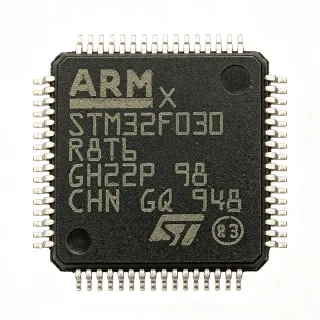
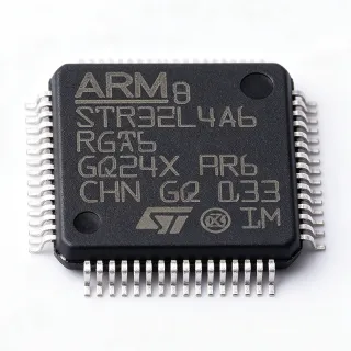
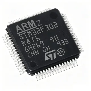
| 패키지 | LQFP-64 (10x10 mm) |
| ADC | 4x 12-bit, up to 5 MSPS |
| DAC | 3x 12-bit |
| Comparators | 7x ultra-fast |
| Operational Amplifiers | 2x on-chip |
| Programmable Gain Amplifiers | 4x |
| Timers | 4x 16-bit + 1x 32-bit |
| Communication | USB 2.0 FS, CAN 2.0B, 3x I2C, 3x SPI, 4x USART, 2x UART |
| 동작 온도 | -40C to +85C |
| RoHS 상태 | Compliant |
| Random Number Generator | True RNG (NIST SP 800-22) |
| I/O Count | 51 GPIO |
| MSL 레벨 | 3 |
STM32F303RCT6 핀 구성
| 핀 1 | PB9 — General-purpose I/O, I2C1_SDA, CAN2_TX, TIM17_BKIN |
| 핀 2 | PC13 — GPIO, RTC_OUT, Tamper-RTC (PC13, PC14, PC15 powered by VBAT) |
| 핀 3 | PC14 — GPIO, OSC32_IN (LSE crystal input) |
| 핀 4 | PC15 — GPIO, OSC32_OUT (LSE crystal output) |
| 핀 5 | OSC_IN — HSE crystal input or external clock input |
| 핀 6 | OSC_OUT — HSE crystal output |
| 핀 7 | NRST — Active-low reset input |
| 핀 8 | VSSA — Analog ground |
| 핀 9 | VDDA — Analog supply (2.4-3.6 V) |
| 핀 10 | PA0 — GPIO, ADC1_IN1, TIM2_CH1, RTC_TAMP2, WKUP1 |
| 핀 11 | PA1 — GPIO, ADC1_IN2, TIM2_CH2, OPAMP1_VINP |
| 핀 12 | PA2 — GPIO, ADC1_IN3, USART2_TX, OPAMP1_VOUT |
| 핀 13 | PA3 — GPIO, ADC1_IN4, USART2_RX, OPAMP1_VINM |
| 핀 14 | PA4 — GPIO, ADC2_IN1, SPI1_NSS, DAC1_OUT1 |
| 핀 15 | PA5 — GPIO, ADC2_IN2, SPI1_SCK, OPAMP2_VINP |
| 핀 16 | PA6 — GPIO, ADC2_IN3, SPI1_MISO, OPAMP2_VOUT, TIM16_CH1 |
| 핀 17 | PA7 — GPIO, ADC2_IN4, SPI1_MOSI, OPAMP2_VINM, TIM17_CH1 |
| 핀 18 | PB0 — GPIO, ADC3_IN3, TIM3_CH3, OPAMP3_VINP (on some revs) |
| 핀 19 | PB1 — GPIO, ADC3_IN4, TIM3_CH4, OPAMP3_VOUT |
| 핀 20 | PB2 — GPIO, ADC2_IN12, BOOT1 |
| 핀 21 | PB10 — GPIO, I2C2_SCL, USART3_TX, TIM2_CH3 |
| 핀 22 | PB11 — GPIO, I2C2_SDA, USART3_RX, TIM2_CH4 |
| 핀 23 | VSS_1 — Digital ground |
| 핀 24 | VDD_1 — Digital supply (2.0-3.6 V) |
| 핀 25 | PB12 — GPIO, SPI2_NSS, I2S2_WS, TIM1_BKIN |
| 핀 26 | PB13 — GPIO, SPI2_SCK, I2S2_CK, TIM1_CH1N |
| 핀 27 | PB14 — GPIO, SPI2_MISO, TIM1_CH2N |
| 핀 28 | PB15 — GPIO, SPI2_MOSI, TIM1_CH3N |
| 핀 29 | PA8 — GPIO, TIM1_CH1, USART1_CK, MCO |
| 핀 30 | PA9 — GPIO, TIM1_CH2, USART1_TX, I2C3_SMBAI |
| 핀 31 | PA10 — GPIO, TIM1_CH3, USART1_RX |
| 핀 32 | PA11 — GPIO, TIM1_CH4, CAN1_RX, USB_DM |
| 핀 33 | PA12 — GPIO, TIM1_ETR, CAN1_TX, USB_DP |
| 핀 34 | PA13 — GPIO, SWDIO (debug data) |
| 핀 35 | VSS_2 — Digital ground |
| 핀 36 | VDD_2 — Digital supply (2.0-3.6 V) |
| 핀 37 | PA14 — GPIO, SWCLK (debug clock) |
| 핀 38 | PA15 — GPIO, TIM2_CH1_ETR, SPI1_NSS |
| 핀 39 | PB3 — GPIO, TIM2_CH2, SPI1_SCK, SWO |
| 핀 40 | PB4 — GPIO, TIM3_CH1, SPI1_MISO, NJTRST |
| 핀 41 | PB5 — GPIO, TIM3_CH2, SPI1_MOSI, I2C1_SMBAI |
| 핀 42 | PB6 — GPIO, TIM4_CH1, USART1_TX, I2C1_SCL |
| 핀 43 | PB7 — GPIO, TIM4_CH2, USART1_RX, I2C1_SDA |
| 핀 44 | BOOT0 — Boot mode selection (main Flash vs System memory bootloader) |
| 핀 45 | PB8 — GPIO, TIM4_CH3, I2C1_SCL, CAN2_RX |
| 핀 46 | VSS_3 — Digital ground |
| 핀 47 | VDD_3 — Digital supply (2.0-3.6 V) |
| 핀 48 | VREF+ — ADC positive reference voltage (tie to VDDA or external reference) |
| 핀 49 | PD2 — GPIO, TIM3_ETR, UART5_RX |
| 핀 50 | PC0 — GPIO, ADC1_IN6, TIM1_CH1 |
| 핀 51 | PC1 — GPIO, ADC1_IN7, TIM1_CH2 |
| 핀 52 | PC2 — GPIO, ADC1_IN8, TIM1_CH3 |
| 핀 53 | PC3 — GPIO, ADC1_IN9, TIM1_CH4, OPAMP4_VINP |
| 핀 54 | PC4 — GPIO, ADC2_IN5, TIM1_CH1N, OPAMP4_VOUT |
| 핀 55 | PC5 — GPIO, ADC2_IN6, TIM1_CH2N, OPAMP4_VINM |
| 핀 56 | PC6 — GPIO, TIM3_CH1 |
| 핀 57 | PC7 — GPIO, TIM3_CH2 |
| 핀 58 | PC8 — GPIO, TIM3_CH3 |
| 핀 59 | PC9 — GPIO, TIM3_CH4 |
| 핀 60 | PA0_WKUP — Wakeup pin (same as PA0, alternate WKUP function) |
| 핀 61 | VBAT — RTC backup supply (1.65-3.6 V) |
| 핀 62 | PC12 — GPIO, TIM1_CH3N, USART3_CK |
| 핀 63 | VSS_4 — Digital ground |
| 핀 64 | VDD_4 — Digital supply (2.0-3.6 V) |
일반적인 애플리케이션
STM32F303RCT6 적합 용도: 6 애플리케이션s: Brushless DC Motor Field-Oriented Control, Industrial PLC and Sensor Conditioning, Digital Power Conversion (PFC and LLC), Medical Patient Monitoring Devices, Building Automation and HVAC Control, Consumer Audio Processing and Smart Speakers.
Brushless DC Motor Field-Oriented Control
The STM32F303RCT6 is purpose-built for BLDC and PMSM motor FOC drives. Its 32-bit advanced timer generates center-aligned complementary PWM with dead-time insertion up to several hundred kHz, while four 12-bit 5 MSPS ADCs sample phase currents and back-EMF in the same PWM cycle. The integrated four PGAs (gain 2 to 16) amplify low-side shunt currents directly into the ADC inputs, eliminating external instrumentation amplifiers. Three 12-bit DACs provide programmable reference voltages for slope compensation or analog setpoints. Seven 25 ns comparators enable hardware overcurrent and desaturation protection that can latch the PWM outputs within a single switching cycle. Typical designs run sensor-less FOC on 24V/48V motors up to 1 kW at 72 MHz, leaving sufficient CPU headroom for speed/torque control loops.
추천
Industrial PLC and Sensor Conditioning
Industrial PLC analog input modules leverage the STM32F303RCT6's four 5 MSPS ADCs with hardware oversampling to achieve effective 14-16 bit resolution for thermocouple, RTD, and 4-20 mA loop measurements. Two on-chip op-amps implement anti-aliasing filters or active transducer excitation directly, while seven comparators trigger fast digital threshold detection for safety interlocks. The 72 MHz Cortex-M4F executes IEC 61131-3 logic with deterministic 1 ms scan times, and the 256 KB Flash stores program plus Modbus/Profibus protocol stacks. CAN 2.0B and four USART blocks interface with industrial fieldbuses without external transceivers. The 2.0 V to 3.6 V supply tolerates 24 V industrial rails via simple LDO front-ends.
추천
Digital Power Conversion (PFC and LLC)
Digital power supplies benefit from the STM32F303RCT6's high-resolution PWM (down to 5.5 ns step with HRTIM-like timer features), four 5 MSPS ADCs for simultaneous input voltage, output voltage, and current sensing, and three DACs for closed-loop analog references. The Cortex-M4F with FPU executes C2000-style control loops (peak current mode, average current mode, FLL) at 72 MHz with sufficient margin for telemetry and PMBus communications. Two on-chip op-amps implement Type-II and Type-III compensation networks for PFC and LLC converters. The TRNG enables secure firmware bootloaders for anti-counterfeiting in field-deployed power systems.
추천
Medical Patient Monitoring Devices
Patient monitors such as pulse oximeters, ECG front-ends, and infusion pumps use the STM32F303RCT6 for its high-resolution ADC acquisition, low-noise analog front-end, and deterministic real-time performance. Four 5 MSPS ADCs oversample ECG channels at 32 kHz and down-sample to 500 Hz with 16-bit effective resolution. Two op-amps implement active instrumentation gain stages for bio-potential signals, while four PGAs adapt to different sensor impedance ranges. The Cortex-M4F DSP extensions run FFT-based heart-rate variability algorithms in real time, and the TRNG provides entropy for HIPAA-compliant session key generation. USB 2.0 Full-Speed enables tethered data upload to clinical software.
추천
Building Automation and HVAC Control
Building automation controllers leverage the STM32F303RCT6's combination of multiple communication interfaces (3x I2C, 3x SPI, 4x USART, 2x UART, CAN, USB) to bridge sensor networks, BACnet/Modbus fieldbuses, and wireless modules. The 256 KB Flash stores BACnet protocol stack plus HVAC control logic, and the 40 KB SRAM supports Modbus TCP buffers. Three DACs generate 0-10 V analog outputs for legacy damper/valve actuators, while four ADCs read thermistor, humidity, and pressure sensors. Two op-amps condition signals from RTDs and 4-20 mA loops. The 72 MHz Cortex-M4F runs multi-loop PID for zone temperature control at 100 ms update rates.
추천
Consumer Audio Processing and Smart Speakers
Audio products from portable speakers to smart-home voice assistants use the STM32F303RCT6 for its three 12-bit DACs (configurable as I2S-compatible with external DAC), three SPI/I2S interfaces for digital microphone arrays, and 72 MHz Cortex-M4F DSP for real-time audio mixing and echo cancellation. The 256 KB Flash stores voice UI firmware plus audio processing pipelines, while the 40 KB SRAM buffers 16 kHz/16-bit audio frames. USB Full-Speed enables direct PC streaming, and CAN/I2C interfaces connect to wireless audio modules and amplifier ICs. The TRNG secures voice-recognition model weights from over-the-air updates.
추천
추천 제품 요약
엔지니어링 참조 데이터: STM32F303RCT6 — 비교, 설계 지침 및 규정 준수 정보.
선택 가이드
대체품과의 비교
| 파라미터 | 이 제품 | STM32F303RCT7 | STM32F303RDT6 | STM32F302RCT6 | STM32F303CCT6 | GD32F303RCT6 |
|---|---|---|---|---|---|---|
| Brand | STMicroelectronics | STMicroelectronics | STMicroelectronics | STMicroelectronics | STMicroelectronics | GigaDevice |
| Package | LQFP-64 (10x10 mm) | LQFP-64 - same | LQFP-64 - same | LQFP-64 - same | LQFP-48 (LQFP-64 variant available) | LQFP-64 - same |
| Core | Cortex-M4F 72 MHz | Cortex-M4F 72 MHz | Cortex-M4F 72 MHz | Cortex-M4F 72 MHz | Cortex-M4F 72 MHz | Cortex-M4F 120 MHz (+67%) |
| Flash | 256 KB | 256 KB | 384 KB (+50%) | 256 KB | 256 KB | 256 KB equivalent |
| SRAM | 40 KB | 40 KB | 48 KB (+20%) | 40 KB | 40 KB | 48 KB |
| DACs | 3x 12-bit | 3x 12-bit | 3x 12-bit | 1x 12-bit (-67%) | 3x 12-bit | 2x 12-bit (-33%) |
| TRNG | Yes | Yes | Yes | No | Yes | No |
| Operating Temperature | -40C to +85C | -40C to +105C | -40C to +85C | -40C to +85C | -40C to +85C | -40C to +85C |
주요 차별점
- Three 12-bit DACs vs one on F302 family (vs STM32F302RCT6)
- Four integrated PGAs (vs STM32F103RBT6)
- FPU and DSP extensions (vs STM32F103RCT6)
- True Random Number Generator (TRNG) (vs GD32F303RCT6)
설계 노트
Provide 100 nF X7R ceramic decoupling on each VDD pin (1, 24, 36, 47, 64) within 3 mm of the pad to suppress switching transients from the 72 MHz core. The VDDA pin (9) should be tied to a clean analog LDO output (e.g., from an AP7331 or TL431) with a 100 nF + 1 uF + 10 uF bulk capacitor stack. The VCAP pins (where present on LQFP-64 variants) require a 1 uF + 100 nF combination for internal regulator stability. Estimated: total bulk decoupling budget is 5x 100 nF + 3x 10 uF per board for this MCU.
The STM32F303RCT6 LQFP-64 has a typical theta_JA of 46 C/W when mounted on a standard JEDEC 4-layer test board. At 72 MHz with all peripherals active, typical power consumption is 38 mA (VDD only, VDDA separate), dissipating approximately 125 mW at 3.3 V - well within the package thermal limits. For industrial environments up to 85 C ambient, no heatsink is required. Add 1 square inch of inner-layer copper pour beneath the LQFP exposed pad (if present) or on the LQFP footprint to reduce theta_JA by approximately 8-10 C/W for safety margin.
Place the HSE crystal (typically 8 MHz fundamental) within 5 mm of OSC_IN/OSC_OUT pins with symmetrical trace lengths and a guard ring tied to GND. The LSE 32.768 kHz crystal for RTC should also be placed close to PC14/PC15 with short traces. Separate analog and digital ground planes with a single point-join beneath VDDA/VREF+ filter caps. Route USB DP/DM differential pair with 90-ohm differential impedance, length-matched within 2 mm. The BOOT0 pin must be pulled down with 10 kohm for normal Flash boot, or pulled up to VDD for System memory bootloader mode - never leave floating.
Do not apply voltage to any GPIO pin before the VDD rail has ramped above 2.0 V, as the internal ESD diodes will forward-bias and latch-up the device. The PA11/PA12 USB DP/DM pins must NOT have external pull-ups or pull-downs when USB is used (the on-chip pull-ups are controllable). When using the DAC outputs as analog references, always enable the DAC buffer and add an external unity-gain buffer op-amp (e.g., MCP6001) for low-impedance drive - the DAC output impedance of approximately 6 kohm otherwise loads the reference voltage. The TRNG requires seeding with entropy from at least two sources before use; consult the application note RM0316 (RNG section) for proper initialization.
When using the high-speed 5 MSPS ADCs, route analog input traces as 50-ohm controlled-impedance microstrips with no vias and a continuous ground reference. Keep ADC traces at least 3x the trace width away from PWM switching signals and digital clock lines. Place a 100-ohm + 1 nF RC anti-aliasing filter at each ADC input pin with the resistor close to the MCU. For motor-control applications with >2 kHz PWM, synchronize ADC sampling to the PWM zero-vector event (using TIM1_TRGO triggers) to avoid sampling during switching transients, which improves effective SNR by 6-8 dB.
규정 준수 정보
Per LCSC and ST product page: RoHS compliant, REACH compliant, MSL Level 3. Not AEC-Q100 qualified - choose STM32F303RCT6TR or STM32F303RCT7 for industrial-plus temperature grades. Halogen-free per ST declaration.